저작자표시-비영리-변경금지 2.0 대한민국 이용자는 아래의 조건을 따르는 경우에 한하여 자유롭게
l 이 저작물을 복제, 배포, 전송, 전시, 공연 및 방송할 수 있습니다. 다음과 같은 조건을 따라야 합니다:
l 귀하는, 이 저작물의 재이용이나 배포의 경우, 이 저작물에 적용된 이용허락조건 을 명확하게 나타내어야 합니다.
l 저작권자로부터 별도의 허가를 받으면 이러한 조건들은 적용되지 않습니다.
저작권법에 따른 이용자의 권리는 위의 내용에 의하여 영향을 받지 않습니다. 이것은 이용허락규약(Legal Code)을 이해하기 쉽게 요약한 것입니다.
Disclaimer
저작자표시. 귀하는 원저작자를 표시하여야 합니다.
비영리. 귀하는 이 저작물을 영리 목적으로 이용할 수 없습니다.
변경금지. 귀하는 이 저작물을 개작, 변형 또는 가공할 수 없습니다.
공학박사 학위논문
High-Performance Solar and Fuel Cells by Design and Fabrication of
Multilevel Multiscale Structures
고효율 태양전지 및 연료전지 시스템 구현을 위한 멀티스케일 다층 구조물 설계 및 제작
2018 년 2 월
서울대학교 대학원
High-Performance Solar and Fuel Cells by Design and Fabrication of
Multilevel Multiscale Structures
Segeun Jang Department of Mechanical and Aerospace Engineering The Graduate School Seoul National University
Abstract
In this thesis, we describe multiscale and multilevel structures with hierarchical patterns via controlled oxygen-inhibition effect of UV-curable materials and creeping behavior of viscoelastic polymer. With the multiscale multilevel structures, we could achieved superpositioned optical properties in mesoscopic dye-sensitized solar cells (DSSCs) and improve device performance of polymer electrolyte membrane fuel cells (PEMFCs) and direct methanol fuel cells (DMFCs).
First, we demonstrate a novel strategy for efficient photon harvesting based on the multilevel multiscale structures (integrated in z-axis direction) prepared by using multiplex lithography for constructing LEGO®-like architectures. In multiplex lithography, stacking of polyurethane acrylate (PUA) membrane with nano- or micro-apertures and additional nano- patterning was enabled by oxygen inhibition effect during photo-
multilevel multiscale PDMS molds were replicated from the multi-staked membrane and its architecture was imprinted on mesoporous TiO2 film by soft molding technique. By various spectral analyses and simulations, advanced light harvesting properties by superposition of optical responses from constituent nano- and micro-patterns were verified. We confirmed the effectiveness of our strategy by applications in dye-sensitized solar cells as a model system, wherein over 17.5% increase in efficiency (by multilevel 400 nm line / 20 μm dot structures) was observed. Also, external quantum efficiencies clearly exhibited that the improved light harvesting was originated from the combined effects of diffraction grating and random scattering induced by both nano- and micro-architectures, respectively.
Next, we suggest a facile and simple multiscale patterning method called creep-assisted sequential imprinting and its application to PEMFC. Based on the creep behavior of a viscoelastic polymer (e.g. Nafion®), we firstly carried out nano-patterning by utilizing thermal imprint lithography above the glass transition temperature (Tg) of the polymer film, and then followed by creep-assisted imprinting with micro-patterns based on the mechanical deformation of the polymer film under the relatively long-term exposure to mechanical stress at temperatures below the Tg of the polymer. The fabricated multiscale arrays exhibited excellent pattern uniformity over large areas (> 3.5 cm x 3.5 cm) and nano-patterns well remained after the second stamping procedure thanks to the creep behavior of Nafion®. Even on the side surface of micro-sized hole-patterns, furthermore, the nano-hole patterns clearly remained. To demonstrate the usage of multiscale architectures, the multiscale Nafion® membranes were incorporated into polymer electrolyte membrane fuel cell and this device showed over 10 % higher performance than conventional one. The enhancement was attributed to mainly two factors; 1. The decrease of mass transport resistance due to unique cone-shape morphology by creep-recovery effects, which generate
the Laplace pressure difference between upper-side and lower-side of droplet and this enables removal of droplet from the catalyst layer easily, 2.
The increase of interfacial surface area between Nafion® membrane and electrocatalyst layer by using multiscale patterned membrane with large surface roughness, which brought increase of electrochemical surface area and higher Pt utilization.
Finally, for achieving high performance DMFC, we present a novel approach to engineer an interface between electrolyte membrane and catalyst layer. In DMFCs, the performance loss mainly resulted from two factors; 1. Slow kinetics of methanol oxidation at the anode, 2. Formation of a mixed potential at the cathode due to methanol crossover through an electrolyte membrane. To resolve both problems, we introduce a multiscale patterned membrane and a guided metal cracked layer between an anode catalyst layer and the membrane by the creep-assisted sequential imprinting and simple stretching technique. The membrane-electrode-assembly with a multiscale patterned membrane showed improved performance owing to enhanced mass transport by the thinned electrode, effective utilization of the active sites, and increased Pt utilization. Further, the electrochemically inactive thin gold layer acted as a physical barrier for methanol crossover and the guided cracks provided multiple proton pathways. From these synergetic effects, our interface engineering utility resulted in an enhancement of the device performance by 42.3% compared with that of the reference.
Contents
Abstract ... ⅰ
List of tables ... vi
List of figures ... vii
Nomenclature ... xiv
Chapter 1. Introduction ... 1 Chapter 2. Oxygen-assisted multiplex lithography and its application to solar cells
2-1. Introduction ∙∙∙∙∙∙∙∙∙∙∙∙∙∙∙∙∙∙∙∙∙∙∙∙∙∙∙∙∙∙∙∙∙∙∙∙∙∙∙∙∙∙∙∙∙∙∙∙∙∙∙∙∙∙∙∙∙∙∙∙∙∙∙∙∙∙∙∙∙∙∙∙∙∙∙∙∙∙∙∙∙∙∙∙∙∙10 2-2. Experimental ∙∙∙∙∙∙∙∙∙∙∙∙∙∙∙∙∙∙∙∙∙∙∙∙∙∙∙∙∙∙∙∙∙∙∙∙∙∙∙∙∙∙∙∙∙∙∙∙∙∙∙∙∙∙∙∙∙∙∙∙∙∙∙∙∙∙∙∙∙∙∙∙∙∙∙∙∙∙∙∙∙∙∙∙14 2-3. Results and Discussion ∙∙∙∙∙∙∙∙∙∙∙∙∙∙∙∙∙∙∙∙∙∙∙∙∙∙∙∙∙∙∙∙∙∙∙∙∙∙∙∙∙∙∙∙∙∙∙∙∙∙∙∙∙∙∙∙∙∙∙∙∙∙∙∙∙∙∙∙∙18
2-3-1. Fabrication of polymeric molds with multiscale multilevel structures by controlling oxygen-inhibition effect ∙∙∙∙∙∙∙∙∙∙∙∙∙∙∙∙∙∙18 2-3-2. Multiscale multilevel designed mesoporous TiO2film ∙∙∙∙∙∙∙∙∙∙∙∙∙23 2-3-3. Super-positioned optical property of multiscale multilevel
TiO2 electrodes∙∙∙∙∙∙∙∙∙∙∙∙∙∙∙∙∙∙∙∙∙∙∙∙∙∙∙∙∙∙∙∙∙∙∙∙∙∙∙∙∙∙∙∙∙∙∙∙∙∙∙∙∙∙∙∙∙∙∙∙∙∙∙∙∙∙∙∙∙∙∙∙∙∙28 2-3-4. Enhanced performance of multiscale architectured dye-
sensitized solar cell ∙∙∙∙∙∙∙∙∙∙∙∙∙∙∙∙∙∙∙∙∙∙∙∙∙∙∙∙∙∙∙∙∙∙∙∙∙∙∙∙∙∙∙∙∙∙∙∙∙∙∙∙∙∙∙∙∙∙∙∙∙∙∙∙∙∙33 2-4. Summary ∙∙∙∙∙∙∙∙∙∙∙∙∙∙∙∙∙∙∙∙∙∙∙∙∙∙∙∙∙∙∙∙∙∙∙∙∙∙∙∙∙∙∙∙∙∙∙∙∙∙∙∙∙∙∙∙∙∙∙∙∙∙∙∙∙∙∙∙∙∙∙∙∙∙∙∙∙∙∙∙∙∙∙∙∙∙∙∙∙∙43 Chapter 3. Creep-assisted sequential imprinting method and its
application to polymer electrolyte fuel cells
3-1. Introduction ∙∙∙∙∙∙∙∙∙∙∙∙∙∙∙∙∙∙∙∙∙∙∙∙∙∙∙∙∙∙∙∙∙∙∙∙∙∙∙∙∙∙∙∙∙∙∙∙∙∙∙∙∙∙∙∙∙∙∙∙∙∙∙∙∙∙∙∙∙∙∙∙∙∙∙∙∙∙∙∙∙∙∙∙∙∙∙45
3-2. Experimental ∙∙∙∙∙∙∙∙∙∙∙∙∙∙∙∙∙∙∙∙∙∙∙∙∙∙∙∙∙∙∙∙∙∙∙∙∙∙∙∙∙∙∙∙∙∙∙∙∙∙∙∙∙∙∙∙∙∙∙∙∙∙∙∙∙∙∙∙∙∙∙∙∙∙∙∙∙∙∙∙∙∙∙∙∙48 3-3. Results and Discussion ∙∙∙∙∙∙∙∙∙∙∙∙∙∙∙∙∙∙∙∙∙∙∙∙∙∙∙∙∙∙∙∙∙∙∙∙∙∙∙∙∙∙∙∙∙∙∙∙∙∙∙∙∙∙∙∙∙∙∙∙∙∙∙∙∙∙∙∙∙51
3-3-1. Creep-assisted sequential imprinting method for constructing multiscale multilevel structures ∙∙∙∙∙∙∙∙∙∙∙∙∙∙∙∙∙∙∙∙∙∙∙∙∙∙∙∙∙∙∙∙∙∙∙∙∙∙∙∙∙∙∙∙∙∙∙∙51 3-3-2. Enhanced performance of polymer electrolyte fuel cell with
Multiscale multilevel designed membrane ∙∙∙∙∙∙∙∙∙∙∙∙∙∙∙∙∙∙∙∙∙∙∙∙∙∙∙∙∙∙∙60 3-4. Summary ∙∙∙∙∙∙∙∙∙∙∙∙∙∙∙∙∙∙∙∙∙∙∙∙∙∙∙∙∙∙∙∙∙∙∙∙∙∙∙∙∙∙∙∙∙∙∙∙∙∙∙∙∙∙∙∙∙∙∙∙∙∙∙∙∙∙∙∙∙∙∙∙∙∙∙∙∙∙∙∙∙∙∙∙∙∙∙∙∙∙∙70
Chapter 4. Interface engineering for high-performance direct methanol fuel Cells
4-1. Introduction ... 71 4-2. Experimental ∙∙∙∙∙∙∙∙∙∙∙∙∙∙∙∙∙∙∙∙∙∙∙∙∙∙∙∙∙∙∙∙∙∙∙∙∙∙∙∙∙∙∙∙∙∙∙∙∙∙∙∙∙∙∙∙∙∙∙∙∙∙∙∙∙∙∙∙∙∙∙∙∙∙∙∙∙∙∙∙∙∙∙∙∙74 4-3. Results and Discussion ∙∙∙∙∙∙∙∙∙∙∙∙∙∙∙∙∙∙∙∙∙∙∙∙∙∙∙∙∙∙∙∙∙∙∙∙∙∙∙∙∙∙∙∙∙∙∙∙∙∙∙∙∙∙∙∙∙∙∙∙∙∙∙∙∙∙∙∙∙80
4-3-1. Fabrication of multiscale patterned membranes ∙∙∙∙∙∙∙∙∙∙∙∙∙∙∙∙∙∙∙∙∙∙∙∙80 4-3-2. Enhanced cell performance of direct methanol fuel cells
with multiscale patterned membranes ∙∙∙∙∙∙∙∙∙∙∙∙∙∙∙∙∙∙∙∙∙∙∙∙∙∙∙∙∙∙∙∙∙∙∙∙∙∙85 4-3-3. Further enhanced cell performance with guided metal
cracked barriers ∙∙∙∙∙∙∙∙∙∙∙∙∙∙∙∙∙∙∙∙∙∙∙∙∙∙∙∙∙∙∙∙∙∙∙∙∙∙∙∙∙∙∙∙∙∙∙∙∙∙∙∙∙∙∙∙∙∙∙∙∙∙∙∙∙∙∙∙∙∙∙∙96 4-4. Summary ∙∙∙∙∙∙∙∙∙∙∙∙∙∙∙∙∙∙∙∙∙∙∙∙∙∙∙∙∙∙∙∙∙∙∙∙∙∙∙∙∙∙∙∙∙∙∙∙∙∙∙∙∙∙∙∙∙∙∙∙∙∙∙∙∙∙∙∙∙∙∙∙∙∙∙∙∙∙∙∙∙∙∙∙∙∙∙∙∙108 References... 109
List of tables
Table 2-1. Loaded dye amounts on flat and patterned mp-TiO2
photoelectrodes
Table 2-2. Detailed J-V characteristics of the DSSCs employing flat or patterned mp-TiO2 photoelectrodes.
Table 2-3. J-V characteristics of the DSSCs employing 800 nm dot, 800 nm line, 800 nm dot / 20 μm dot, or 800 nm line / 20 μm dot patterned mp-TiO2 photoelectrodes.
Table 4-1. Open circuit voltage, current density at 0.4 V, and maximum power density of prepared MEAs at two different methanol concentrations (1.5 M and 3.0 M)
List of Figures
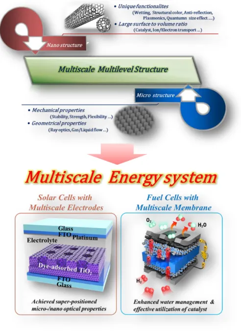
Figure 1-1. Brief introduction of the effects of multiscale structures which consists of nano- and micro- structures and its applications for improved optical properties of solar cells and high performance fuel cells
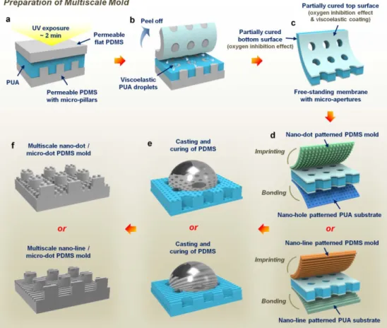
Figure 2-1 Schematic illustration describing the procedure for preparation of multilevel multiscale PDMS molds by multiplex lithography and replication.
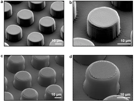
Figure 2-2. SEM images of multilevel multiscale PDMS molds. (a,b) 400 nm dot / 20 μm dot patterned PDMS at (a) low and (b) high magnifications. (c,d) 400 nm line / 20 μm dot patterned PDMS at (c) low and (d) high magnifications.
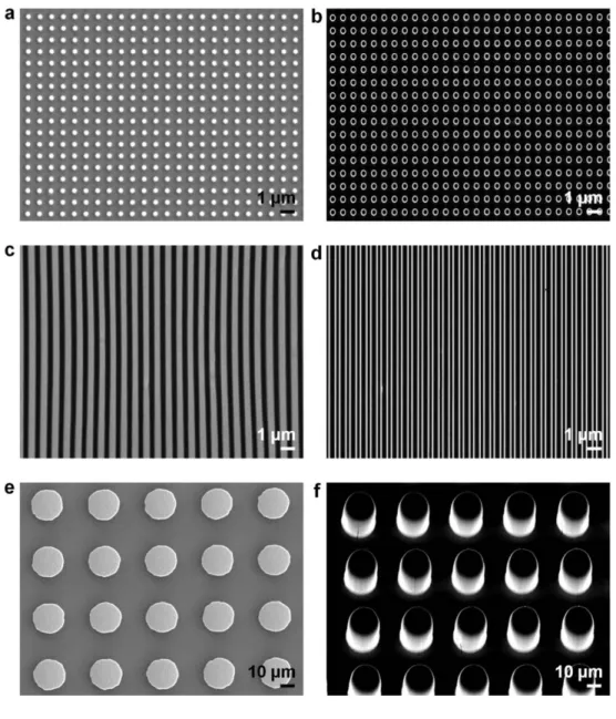
Figure 2-3. SEM images of (a,b) 400 nm dot, (c,d) 400 nm line, (e,f) 20 μm dot patterned PDMS molds. The images were obtained by using either (a,c,e) secondary electron (SE2) detector or (b,d,f) in-lens detector.
Figure 2-4. Schematic illustration describing the methods for preparation of patterned mp-TiO2 film by soft molding technique.
Figure 2-6. (a) Digital photographs of flat (noted as Reference) and patterned (detailed architectures noted at each image) mp- TiO2. (b) Reflectance spectra of flat and patterned mp-TiO2.
Figure 2-7. Calculated light reflection enhancement of patterned mp- TiO2 compared to flat mp-TiO2 from FDTD simulation.
Figure 2-8. (a) Digital photographs of flat and patterned mp-TiO2 with dye-sensitization. (b) Absorbance spectra of flat and patterned mp-TiO2 with dye-sensitization.
Figure 2-9. (a,b) J-V characteristics and (c,d) IPCE spectra of DSSCs employing mp-TiO2with (a,c) flat, 400 nm dot, 20 μm dot, and 400 nm dot / 20 μm dot patterns and (b,d) flat, 400 nm line, 20 μm dot, and 400 nm line / 20 μm dot patterned structures.
Figure 2-10. Top-view SEM images of (a) 800 nm dot, (b) 800 nm line, (c) 800 nm dot / 20 μm dot, and (d) 800 nm line / 20 μm dot patterned mp-TiO2 films. The insets show enlarged images taken at higher magnifications.
Figure 2-11. J-V characteristics of DSSCs employing (a) 800 nm dot and 800 nm dot / 20 μm dot patterned photoelectrodes and (b) 800 nm line and 800 nm line / 20 μm dot patterned mp-TiO2
films. Results of flat (noted as Reference) and 20 μm dot patterned samples are displayed for comparisons.
Figure 3-1. Schematic illustration for fabrication process of multiscale Nafion membrane with sequential imprinting. (a) Imprinting nano-patterns on bare Nafion membrane under the above glass temperature condition (Tg). (b) Sequential- imprinting micro-patterns on nano-patterned Nafion membrane under the below glass temperature condition
(Tg). (c) Replicating the multiscale-patterns with PUA from the multiscale Nafion membrane. (d-f) The corresponding digital camera images for nano-patterned Nafion membrane (d), multiscale Nafion membrane (e), and replicated multiscale PUA mold (f).
Figure 3-2. (a) The SEM image for nano-patterned Nafion membrane.
(b-d) The SEM images for the obtained structures after sequential-imprinting with the stamping temperature variation of second imprinting process. (b) ~80 °C, (c)
~100 °C, and (d) ~120 °C. (e) The SEM image for replicated multiscale PUA mold. (f) The cross-sectional SEM image for the catalyst layer on multiscale Nafion membrane.
Figure 3-3. Fabricated multiscale Nafion membrane and PUA 311 mold with combination of the micro pillar-patterns and the nano line-patterns.
Figure 3-4. Fabricated multiscale Nafion membrane and PUA 311 mold with combination of the micro line-patterns and the nano dot-patterns
Figure 3-5. Fabricated multiscale Nafion membrane and PUA 311 mold with combination of the micro line-patterns and the nano line-patterns
Figure 3-6. Schematic illustrations for creep response of Nafion membrane (a), instantaneous creep recovery effect during
membrane under the conditions of H2/Air (a) H2/O2 (b) under ambient pressure and H2/Air under pressure of 150 kPa (c). (d) The oxygen gain obtained under ambient pressure.
Figure 3-8. Single-cell performance of the MEAs with various pattern dimensions in the conditions of H2/Air under ambient pressure
Figure 3-9. (a) Equivalent circuit of the PEMFC single cell (LW = inductance of the electric wire, Rmembrane = internal membrane resistance, Rcathode (anode) = charge transfer resistance of the cathode (anode), CPEcathode (anode) = constant phase element of the cathode (anode) and ZW = Warburg impedance). (b) Electrochemical impedance spectroscopy (EIS) of a conventional MEA and MEA with the multiscale Nafion membrane at 0.5 V. (c) Schematic illustration for the force balancing of a water droplet at a cone-shaped void space in a catalyst layer.
Figure 3-10. The contact angle of a DI water droplet on the cathode catalyst layer
Figure 3-11. (a) Cyclic voltammogram (CV) of the cathode catalyst layers of a conventional MEA and MEA with the multiscale Nafion membrane. (b) Increased surface area ratio compared to flat surface with various patterned surfaces.
Figure 4-1. Schematic for the fabrication of the multiscale prism- patterned membrane by thermal imprinting.
Figure 4-2. SEM images of the surface of the multiscale prism- patterned mold.
Figure 4-3. SEM images of the surfaces of the (a) flat reference, (b) prism-patterned (P-10), and (c) multiscale prism-patterned (MP-10) membranes; FIB-assisted cross-sectional SEM images of the anode catalyst layers of the prepared CCMs with a (d) flat surface, (e) prism pattern (P-10), and (f) multiscale prism pattern (MP-10).
Figure 4-4. AFM images of the surface of the prism-patterned (P-10) and multiscale prism-patterned (MP-10) membranes.
Figure 4-5. Relative membrane-electrode interface area of the flat reference, prism-patterned (P-10) and multiscale-patterned (MP-10) membrane.
Figure 4-6. (a–b) Single cell polarization curves and (c–d) EIS spectra of the reference MEA, MEAs with patterned membranes (P-10 and MP-10), and MEAs with patterned membranes containing a Au layer with guided cracks (P-10-Au and MP- 10-Au).
Figure 4-7. (a) Anode polarization curves and (b) anode EIS spectra of the reference MEA and MEAs with prism- (P-10) and multiscale prism-patterned (MP-10) membranes.
Figure 4-8. Single cell polarization curves under hydrogen-oxygen operation of all the MEAs including MEAs with patterned- membranes (P-10 and MP-10) and MEAs with patterned- membranes containing a Au layer with guided cracks (P-10- Au and MP-10-Au)..
Figure 4-10. (a) Schematic for generating guided Au cracks by simple mechanical stretching (strain of ~0.25) and (b) SEM images of the surfaces of prism-patterned (P-10-Au) and multiscale prism-patterned (MP-10-Au) membranes with guided Au cracks.
Figure 4-11. Limiting current density measurements for the reference MEA, MEAs with patterned membranes (P-10 and MP-10), and MEAs with patterned membranes and a guided Au cracked layer (P-10-Au and MP-10-Au).
Figure 4-12. Cyclic voltammogram (CV) of the anode catalyst layers of all the MEAs including MEAs with patterned-membranes (P-10 and MP-10) and MEAs with patterned-membranes containing a Au layer with guided cracks (P-10-Au and MP- 10-Au).
Figure 4-13. Schematic illustration of the effects of the enlarged interfacial area and the guided Au cracked barrier.
Figure 4-14. Single cell polarization curves under the 1.5 M methanol- oxygen (or air) operation of reference MEA and multiscale patterned MEA with Au layer with guided cracks (MP-10- Au). The flow rate of oxygen and air were identical (200 ml min-1).
Figure 4-15. (a) Single cell polarization curves and (c) EIS spectra of the MEAs including reference MEA, MEA with intact Au layer (Intact Au), MEA with randomly cracked Au layer (Random Au) and MEAs with patterned membranes containing a Au layer with guided cracks (P-10-Au and MP-10-Au).
Figure 4-16. SEM images of the surfaces of the intact Au layer and randomly cracked Au layer on flat membrane.
N omenclature
λ Wavelength
n The real parts of the refractive index k The imaginary parts of the refractive index
ΔPL Laplace pressure
γ Surface tension
R Radius of curvature
Tg Glass temperature
𝐸𝐸0 Standard potential
F Faraday’s constant
𝑎𝑎 Chemical activity
Chapter 1. Introduction
Multiscale hierarchical structures, the combined structures of micro- and nano-scale repeated pattern, have received great attention due to their unique functions and structural advantages from individual micro- and nano-scale morphology simultaneously1-5. Generally, microstructures provide enhanced mechanical properties (e.g., stability, strength, and flexibility)6 and geometrical effects such as controlled optical pathlength7-8 and gas/liquid flow9. Whereas nanostructures exhibit unique functionalities including plasmonic effects10, quantum size effects11, anti-reflection characteristics12 and structural color6 as well as excellent catalytic13 and ion/electron transport properties14 due to the large surface to volume ratio characteristic. Examples are abundantly found in natures including self- cleaning function of lotus leaves with super-hydrophobicity6, directional adhesion property of gecko feet15, anti-reflection effect of moth-eye12, and structural color of morph butterfly wings16, and some mechanically reinforced multiscale structures such as exoskeleton of the sheep crab5 and flexible dermal armor of the arapaima fish17. Based on these intriguing properties of multiscale structures that provide multifunctional properties to
conventional multiscale-patterning processes, however, introducing the nano-scale patterns both on the top and bottom side of micro-patterns and multi-level structuring are hard to achieve22-24.
Solar cells has been considered as one of the most promising candidates to replace fossil fuels, which suffer from limited quantities and environmental issues25. Especially, low-cost photovoltaics based on nanostructured oxide semiconductors and inorganic/organic light absorbers (e.g. mesoscopic sensitized solar cells and perovskite solar cells) are gaining great interests as promising alternatives to conventional silicon solar cells due to their low manufacturing costs, relatively high energy conversion efficiencies and the steep performance increase26-28.In these types of solar cells, charge collection and light harvesting properties of the nano-oxide (typically TiO2) films are among the most important factors that determine the overall energy conversion efficiency29. Until now, various attempts have been made on improvement of light harvesting in mesoscopic dye-sensitized solar cells (DSSCs) by employing patterned structures on the mp-TiO2
electrodes30-32. However, these patterning techniques have intrinsic limitation that the insertion of periodic architectures is confined to the single-level 2-dimensional structures.
Similarly, much attention has been paid to fuel cells as promising efficient and non-polluting power sources because they offer higher energy densities and energy efficiencies compared to other current/conventional
systems33-35. Fuel cells are electrochemical energy conversion systems that transform the chemical energy of a fuel (e.g. hydrogen, methanol, etc.) and an oxidant (air or oxygen). Among the fuel cell systems, Polymer electrolyte membrane fuel cells (PEMFC) and direct methanol fuel cells (DMFC) have extensively studied for automotive applications36 and portable power- sources35. Nonetheless, to commercialize PEMFC and DMFC, some obstacles, such as water management in PEMFC, methanol crossover problems in DMFC and high-cost of Pt catalyst in both systems, need to be overcome34-35. To resolve the issue of methanol crossover, many approaches have been adopted, such as developing organic/inorganic composite membranes37-38 and embedding a methanol barrier layer into the membrane surface39-40. To resolve other issues, namely Pt utilization and water management, many studies have examined the incorporation of a patterned membrane into fuel cell devices using a simple one-dimensional micro- /nano pattern. An enlarged interfacial area between the anode and the electrolyte membrane using nano-patterned membrane resulted in higher Pt utilization of fuel cells41-42. Also, micro-patterned membrane showed enhanced water transport property by introducing macro-void between electrode and gas diffusion layer (GDL)34, 43. However, using these simple
been challenging by simple composite membrane due to methanol permeation resulting from the electro-osmotic drag caused by hydrated protons and diffusion.
To address the remained issues and overcome the limitations, we have developed two novel and facile methods to achieve multilevel multiscale structures; 1. Oxygen-assisted multiplex lithography42, which employs partially cured polymeric membrane as a basic brick to be implemented in a vertical stacking and bonding procedure, 2. Creep-assisted sequential imprinting technique, which consists of the first step of thermal imprinting with nano patterns and the following step of imprinting with micro patterns utilizing the creeping behavior of viscoelastic polymer. With the multilevel multiscale structures, we could achieve enhanced optical properties in DSSCs and improved device performance of PEMFC and DMFC. In DSSCs, we performed investigations on photonic application of multilevel multiscale patterned nano-oxide photoelectrodes for efficient light harvesting. The z-axis integration of nano- and micro-patterns resulted in superpositioned optical responses from nano- and micro-scale structures, enabling synergistic photon trapping within the photoelectrode by simultaneous diffraction grating and light scattering. In addition, in PEMFC, the multilevel multiscale patterned membranes, where the nanopatterns covered the whole surface even on the side surface of microstructures, have brought significantly improved device performance. The enhancement was
attributed to the decrease of mass transport resistance due to unique morphology of micro-patterns by creep-recovery effects and the increase of interfacial surface area between membrane and electrocatalyst layer.
Furthermore, in DMFC, the multiscale patterned membrane resulted in enhanced performance by improving mass transport, active site utilization, and Pt utilization. Also, additionally incorporated a guided gold cracked layer effectively reduced the methanol crossover rate while maintaining the proton transport ability owing to the existence of multiple cracks.
Figure 1-1. Brief introduction of the effects of multiscale structures which consist of nano-/micro-structures and its applications for improved optical properties of solar cells and high performance fuel cells
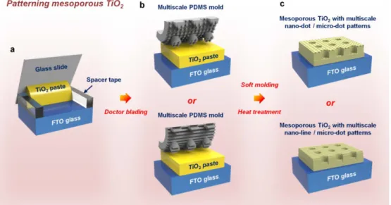
In Chapter 2, we demonstrate a strategy for efficient photon harvesting based on the multilevel multiscale structures prepared by using multiplex lithography for constructing LEGO®-like architectures. Multilayer assembly of polyurethane acrylate (PUA) films with nano- or micro- apertures (or patterns) was enabled by oxygen-assisted partial curing of PUA resin. Based on the different amount of uncured degree of PUA films between the bottom and top surface, partially cured bottom surface of PUA film was used for adhesion to micro- or nano- patterned PUA membrane while proper nanostructures were imprinted on the relatively less cured top surface of the PUA. After, PDMS molds with multilevel structures comprising nano- and micro-structures projected on the whole surface were replicated. Then, mesoporous (mp)-TiO2 films with multilevel nano- and micro-patterns were prepared by using one-step elastomer stamping method.
Various optical measurements and simulations were performed in order to confirm the optical characteristics of our multilevel multiscale structures, and superpositioned optical interferences induced by periodic nano-patterns and micro-patterns were observed. We verified the effectiveness of our approach by utilizing patterned mp-TiO2 film in DSSCs. Under standard 1 sun illumination, over 17.5 % enhancement in energy conversion efficiency
In Chapter 3, we suggest a facile and simple multiscale patterning method called creep-assisted sequential imprinting and its application to PEMFC. The creep behavior is the phenomenon of a solid material to be deformed permanently even below the glass temperature under the long- term exposure to mechanical stresses. By using this creep behavior, we sequentially imprinted nano- and micro-scale patterned-mold onto a viscoelastic polymer film: the first step of thermal imprinting with nano patterns and the following step of creep-assisted imprinting with micro patterns and finally, replicating step through casting and UV curing of PUA on the patterned film was performed. The completed multiscale mold shows the nano-patterns well remained after the second stamping procedure thanks to the creep behavior of Nafion. Interestingly, even on the side surface of micro-sized hole-patterns, the nano-patterns clearly remained. For verifying the practical usage of multiscale structures, multiscale patterned membrane was incorporated into PEMFC. With micro-patterns in multiscale patterned membrane, regular empty space was formed in catalyst layer and showed positive effect on mass transfer in cathode side. In addition, the enlarged interfacial surface between catalyst layer and patterned membrane resulted in high Pt utilization. The combined effects of improved mass transport and increase of Pt utilization brought improved device performance of PEMFC.
In Chapter 4, we propose interface engineering method to introduce a multiscale patterned membrane and a guided metal cracked layer in
DMFC by the creep-assisted sequential imprinting and simple stretching technique. Using the creep-assisted sequential imprinting method, we easily fabricated a multiscale hierarchical-structured membrane with a high surface area. The device with the multiscale patterned membrane showed improved performance compared with that of the reference because mass transport was enhanced by the thinned electrode and the effective utilization of catalytic active sites. Moreover, the electrochemically inactive thin gold layer was expected to act as a physical barrier for methanol crossover and the guided cracks provided multiple proton pathways. By combining synergetic effects of higher Pt utilization, enhanced mass transport and reduced methanol crossover, the device performance of DMFC was significantly enhanced by 42.3% compared with that of the reference.
Chapter 2. Oxygen-assisted multiplex lithography and its application to solar cells
Published in Advanced Functional Materials, 2016, 26, 6584
2-1. Introduction
Among various sustainable energy sources, solar energy has been considered as one of the most promising candidates to replace fossil fuels, which suffer from limited quantities and environmental issues25. Though being challenged by demands on high energy density, recent advances on the development of highly efficient photovoltaics are raising the expectations for large scale practical utilization of solar energy44. Especially, low-cost photovoltaics based on nanostructured oxide semiconductors and inorganic/organic light absorbers (e.g. mesoscopic sensitized solar cells and perovskite solar cells) are gaining great interests due to the steep rise in performance26-28, 45-53
. In these types of solar cells, charge collection and light harvesting properties of the nano-oxide (typically TiO2) films are among the most important factors that determine the overall energy conversion efficiency29. Significant progress in charge collection was achieved by structural engineering of oxides, however, trade-off between minimizing the traveling distance of excitons and maximizing the surface area for efficient utilization of incident photons caused limitations to further
advances54-61. In contrast, significant improvements were made by tailoring the optical characteristics of nano-oxide films62-63. Various types of approaches such as elongation of light pathways within the oxide film (light trapping) by incorporation of light scattering materials64-67 or photonic crystals68-73 have been reported, and insertion of metallic nano-architectures for surface plasmon resonance has delivered significant enhancements74-78.
On the basis of understanding on the optical properties of periodic nanostructures, Kim et al. reported nano-line patterned mesoporous TiO2
(mp-TiO2) film fabricated by imprinting the nano-lines on mp-TiO2 by using a polydimethylsiloxane (PDMS) mold. Diffraction gratings induced by the patterns within the photoelectrode substantially enhanced light harvesting properties, which led to significantly increased efficiency in dye- sensitized solar cells (DSSCs)79. Micro-patterned mp-TiO2 photoanodes for DSSCs were reported shortly after, and prolonged light pathways due to the reflections at TiO2/electrolyte interfaces with ~25 μm-sized patterns were verified by experimental results and optical simulations80. Until now, various attempts have been made on improvement of light harvesting in mesoscopic solar cells by employing patterned structures on the mp-TiO2
electrodes30-31, 81-84
. However, these patterning techniques have intrinsic
alignments of multilayer nano-lines with 45° or 90° tilting), and verified the effectiveness of their strategy by achieving enhancements in light harvesting, which resulted from diffraction grating-induced multiple reflections32. Though this elaborate technique to overcome the limitation is highly appreciable, multi-layering procedure of mesoporous oxide film comprises numerous and complicated steps which hinder practical utilization of this method.
Herein, we demonstrate a strategy for efficient photon harvesting based on the multilevel multiscale structures prepared by using multiplex lithography for constructing LEGO®-like architectures42. Multilayer assembly of polyurethane acrylate (PUA) films with nano- or micro- apertures (or patterns) was enabled by UV-curable properties of PUA85, and PDMS films with multiscale patterns comprising nano- and micro-structures projected on the whole surface were replicated. Then, mp-TiO2 films with multilevel nano- and micro-patterns were prepared by using one-step elastomer stamping method, which is a feasible and reliable procedure86. Various optical measurements and simulations were performed in order to confirm the optical characteristics of our multilevel multiscale structures, and superpositioned optical interferences induced by periodic nano- patterns87-89 and micro-patterns90-91 were observed. We verified the effectiveness of our approach by utilizing patterned mp-TiO2 film in DSSCs, which served as a model system. Under standard 1 sun illumination, over
17.5 % enhancement in energy conversion efficiency primarily caused by increased photocurrent density was achieved. Also, by comparing the incident photon-to-current efficiency (IPCE) with optical measurement results, we could confirm that the improved light harvesting in the optoelectronic device has been originated from the manifestation of overlapped optical enhancements aroused from nano- and micro-patterns.
2-2. Experimental
Fabrication of Multilevel Multiscale Patterned PDMS Molds by Multiplex Lithography
A small amount of hydrophilic polymer resin (PUA311; Minuta Tech.) was dispensed onto a 20 μm pillar PDMS mold, and a flat PDMS blanket was placed on the top, uniformly covering the patterned PDMS mold by conformal contact. Then this sandwich-like assembly was exposed to UV light (λ = 250 - 400 nm) for a short time (< 2 min) under an applied pressure (~500 g/cm2) for partial curing of PUA. After obtaining the free- standing PUA membrane with 20 μm aperture, uncured part of this membrane at the bottom surface was used for adhesion to a 400 nm hole or 400 nm line patterned PUA membrane. Also, 400 nm dot or 400 nm line patterns were imprinted on the unpolymerized top surface of the PUA, by irradiating UV light (> 5 min, λ = 250-400 nm) with hydraulic pressure (10 kg/cm2) in a vacuum chamber (5×10⁻² Torr). After removal of the PDMS mold, a PUA with multiscale and multilevel (-) patterned structure was formed. This PUA substrate was used for the replication of PDMS film with multilevel multiscale (+) patterns. A mixture of base and curing agents (10:1 w/w) of PDMS (Sylgard 184, Dow Corning) was dispensed into PUA substrate and cured at 70°C for 1.5 h, and the multilevel multiscale PDMS mold was obtained by peeling off the PDMS from the PUA.
Preparation of Multiscale and Multilevel Multiscale Patterned mp-TiO2 Photoelectrodes and DSSCs.
A compact TiO2 blocking layer was deposited onto the FTO glasses (TEC-8, Pilkington) by dipping the glasses in a 40 mM TiCl4 aqueous solution at 70 ºC for 30 min. Then, commercial colloidal TiO2 paste (DSL 18NR-T, Dyesol) with neutral pH was cast onto the FTO substrate by doctor-blading method. Then, multilevel multiscale PDMS mold was placed onto the TiO2 film and was gently pressed, followed by drying process at 70 °C for 20 min. The PDMS mold was then detached from the TiO2 film, and the TiO2 nanoparticle paste on the FTO was annealed at 500 °C in air for 30 min. After TiCl4 post-treatment for increased dye-loading and charge injection92, sintered TiO2 nanoparticles were dye-sensitized by dipping the film in the ethanolic solution of 0.5 mM N719 dye (Ruthenizer 535-bis TBA, Solaronix) at 30 °C for 48 h. Platinized FTO electrode prepared by thermal decomposition was used as counter electrode for DSSCs, and a 50 μm thick thermoplastic sealent (Surlyn, DuPont) was used for cell assembly93. Then, I3-
/I- redox electrolyte composed of 0.6 M 1-butyl-3-methylimidazolium iodide, 30 mM I2, 0.1 M guanidinium thiocyanate, and 0.5 M 4-tert- butylpyridine in a mixture of acetonitrile and valeronitrile (volumetric ratio
Physical and Electrochemical Measurements
SEM images were obtained by using Carl Zeiss MERLIN compact, and optical measurements were performed with Perkin-Elmer Lambda 45 spectrophotometer. Evaluations of photovoltaic performances were done by using a solar simulator (XIL model 05A50KS source measure units, SERIC Ltd.) which was calibrated to a 1 sun condition (AM 1.5G with an incident light intensity of 100 mW/cm2) based on a standard Si solar cell certified by National Institute of Advanced Industrial Science and Technology (AIST, Japan). A potentiostat (Solartron 1480) was used for measurements of J-V characteristics, and IPCE spectra were obtained with QEX7 manufactured by PV Measurements.
Optical Simulations
Full-wave electromagnetic simulation was performed by using Lumerical FDTD simulation software (www.lumerical.com). The simulation structure was based on the experimental observations on the actual single-level and multilevel patterned mp-TiO2 electrodes based on SEM analyses (Figure 2-7). The real parts (n) of the refractive indices of the mp-TiO2 and glass substrate layers were chosen to be 2.258 and 1.34, respectively, while the imaginary parts (k) of the refractive indices were both set to zero by assuming lossless layers. The plane wave source with a wavelength ranging from 350 nm to 700 nm was placed inside the glass
substrate and impinged along the z-direction (vertical direction to the device structure). The periodic boundary conditions for x-axis, y-axis, and the perfectly matched layer for z-axis were imposed on the unit-cell structure.
Then, the spectral reflectances of the single- and multilevel patterned electrodes were compared with that of the flat electrode.
2-3. Results and Discussion
2-3-1. Fabrication of polymeric molds with multiscale multilevel structures by controlling oxygen-inhibition
Preparation of multilevel multiscale PDMS mold was performed according to the procedures described in Figure 2-1. First, fabrication of flexible and free-standing PUA membrane with 20 μm apertures was performed. After the deposition of polymer resin (PUA311, Minuta Tech.) onto a PDMS mold with 20 μm pillar-patterns, a flat PDMS blanket was placed on the top, and the sandwiched assembly was exposed to a short UV irradiation for partial curing of the PUA (Figure 2-1a). Since the permeable PDMS can let oxygen penetrate through the PDMS layer94, uncured thin layers were formed at top and bottom surfaces of the PUA membrane due to oxygen inhibition effect95. Also, because of the low affinity between the hydrophilic PUA and hydrophobic PDMS surface, the uncured resin droplets on the PDMS pillars escape to the top surface of PUA film during the removal of PDMS blanket and form a viscoelastic coating on the PUA (Figure 2-1b and 1c)42, 96. This enables additional imprinting on the top surface with nanopatterned PDMS mold and additional integration of PUA membrane at the bottom. Based on these properties of the PUA membrane, LEGO®-like monolithic integration was performed at the bottom of the membrane by putting the membrane onto a film with 400 nm hole or 400
nm line patterns. Simultaneously, imprinting on the top of the membrane was carried out by pressing with 400 nm dot or 400 nm line patterned PDMS mold (Figure 2-1d). Then the PDMS film with multilevel multiscale architecture was prepared by performing replication by casting and curing of PDMS pre-polymer onto the integrated multiscale PUA substrate (Figure 2- 1e and 1f).
Figure 2-2 shows the scanning electron microscope (SEM) images of multilevel 400 nm dot / 20 μm dot (Figure 2-2a and 2b) and 400 nm line / 20 μm dot (Figure 2-2c and 2d) patterned PDMS films, and it is clearly observable that the multilevel multiscale molds have been successfully prepared with high pattern fidelity. Periodic nano-dots or nano-lines were not only present on top of the micro-pillars but also on the floor, enabling both nano- and micro-patterns to be imprinted on the whole surface by complete overlap of nano- and micro-patterns in z-axis direction. In order to investigate the characteristics of multilevel multiscale periodic structure, single-level 400 nm dot, 400 nm line, and 20 μm dot patterned PDMS molds were also prepared for proper comparisons between single- and multilevel architectures. The SEM images of single-layer patterned PDMS molds are displayed in Figure 2-3.
Figure 2-1. Schematic illustration describing the procedure for preparation of multilevel multiscale PDMS molds by multiplex lithography and replication.
Figure 2-2. SEM images of multilevel multiscale PDMS molds. (a,b) 400 nm dot / 20 μm dot patterned PDMS at (a) low and (b) high magnifications.
(c,d) 400 nm line / 20 μm dot patterned PDMS at (c) low and (d) high magnifications.
Figure 2-3. SEM images of (a,b) 400 nm dot, (c,d) 400 nm line, (e,f) 20 μm dot patterned PDMS molds. The images were obtained by using either (a,c,e) secondary electron (SE2) detector or (b,d,f) in-lens detector.
2-3-2. Multiscale multilevel designed mesoporous TiO
2film
The multilevel multiscale patterned mp-TiO2 electrodes were prepared by the soft-molding method described in Figure 2-4. First, commercial viscous TiO2 paste (DSL 18NR-T, Dyesol) was casted onto fluorine-doped tin oxide (FTO) glass substrate by doctor-blade method (Figure 2-4a). Then, the multiscale PDMS mold with 400 nm dot / 20 μm dot or 400 nm line / 20 μm dot structures was placed onto the TiO2 film with a gentle pressure, followed by thermal annealing at 70 °C for 20 min to remove the residual solvent (Figure 2-4b). After detaching the PDMS mold, heat treatment was performed at 500 °C for 30 min for sintering of TiO2 nanoparticles and calcination of organic binders. Consequently, mp-TiO2 films on FTO glasses with multilevel multiscale patterns on the top-surface were obtained (Figure 2-4c). Flat and single-level (400 nm dot, 400 nm line, and 20 μm dot) patterned mp-TiO2 electrodes were also prepared for comparisons.
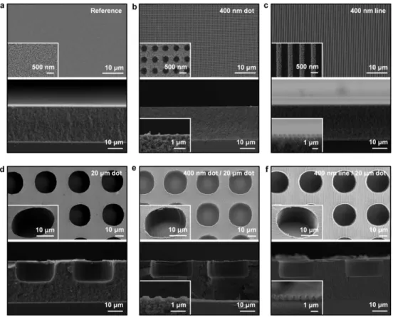
The morphologies of the patterned mp-TiO2 electrodes were observed by SEM analyses. Figure 2-5a-5d show top-view and cross-sectional SEM images of flat, 400 nm dot, 400 nm line, and 20 μm dot patterned mp-TiO2
films, respectively. The nanostructures were uniformly imprinted onto the
μm dot and 400 nm line / 20 μm dot patterned mp-TiO2 films of which morphologies are visualized by SEM and displayed in Figure 2-5e and Figure 2-5f, respectively. From the high magnification images in the insets, it is clear that the periodic structures of 400 nm dots or 400 nm lines are neatly imprinted on the surface including micro-patterned regions. Also, we measured the areal dye-loading in order to examine the influences of patterning on the effective surface areas of mp-TiO2. The differences in the numbers of loaded dye molecules on flat and patterned mp-TiO2 films were within 3.5% (see Table 2-1 for details), indicating that the imprinting procedures caused negligible changes to the surface area. Moreover, viability of these patterning techniques for scaling-up, which is an important aspect for practical applications, was confirmed by preparation of single- and multilevel patterned mp-TiO2 photoelectrodes with a dimension of 3 cm
× 3 cm as a model size. The digital photographs of the scaled-up TiO2 films before and after dye-sensitization are shown in Figure 2-6a and Figure 2-8a, respectively.
Figure 2-4. Schematic illustration describing the methods for preparation of patterned mp-TiO2 film by soft molding technique.
Figure 2-5. Top-view and cross-sectional SEM images of (a) flat, (b) 400 nm dot, (c) 400 nm line, (d) 20 μm dot, (e) 400 nm dot / 20 μm dot, and (f) 400 nm line / 20 μm dot patterned mp-TiO2.
Sample Dye-loading (× 10-7 mol/cm2)
Reference 5.35
400 nm dot 5.20
400 nm line 5.21
20 μm dot 5.18
400 nm dot / 20 μm dot 5.36
400 nm line / 20 μm dot 5.29
Table 2-1. Loaded dye amounts on flat and patterned mp-TiO2 photoelectrodes.
2-3-3. Super-positioned optical property of multiscale multilevel TiO
2electrodes
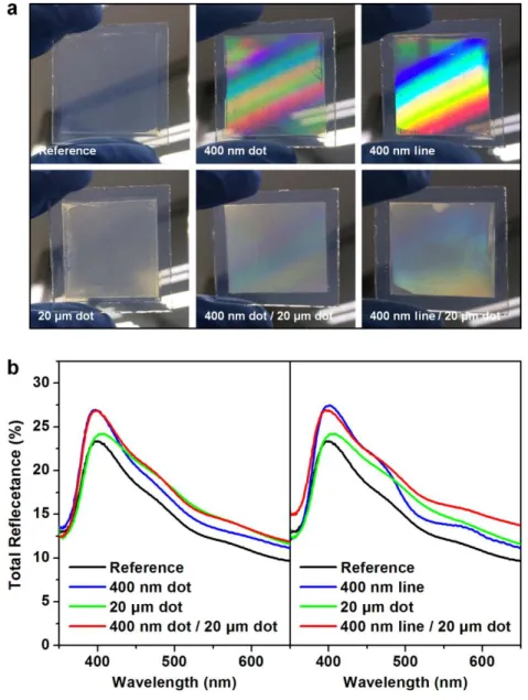
The distinct optical characteristics of the flat, single-level, and multilevel multiscale patterned mp-TiO2 films on FTO glass substrate were first observed with bare eyes. As can be seen from the photos displayed in Figure 2-6a, mp-TiO2 with periodic 400 nm patterns exhibited iridescent colors which can be attributed to the diffraction gratings within visible light wavelength region. In contrast, light scattering in random directions were present in micropatterned mp-TiO2, which can be identified by significantly decreased transparency. Since neither of these optical behaviors are present in the flat mp-TiO2 film (noted as Reference in Figure 2-6a), the observations in patterned TiO2 are ascribable to the nano- and micro- architectures. Interestingly, both of the optical effects were observable in mp-TiO2 with multilevel multiscale patterns, implying the co-existence of photonic properties induced by both 400 nm (diffraction grating) and 20 μm (light scattering) dimensions in multiscale mp-TiO2 film, wherein nano- and micro-structures are completely integrated in z-axis direction.
Then, reflectance measurements were performed in visible light wavelength region for quantitative investigations on the optical properties of multilevel multiscale architectures. Figure 2-6b shows the reflectance spectra of the flat and patterned mp-TiO2 photoanodes, which were measured by light irradiation from the glass side considering the potential
photovoltaic applications. Compared to the flat mp-TiO2, single-level 400 nm dot and 400 nm line patterned mp-TiO2 films exhibited enhanced reflectivity over the wavelength range of 350 nm to 700 nm, especially to a large extent in a relatively short wavelength region below 500 nm. On the contrary, single-level 20 μm dot patterned TiO2 film exhibited increased reflectance at the wavelengths higher than 400 nm, and its magnitude beyond the wavelength of 500 nm became larger than that of 400 nm dot and 400 nm line patterned cases. As have been expected from the examinations on digital photographs in Figure 2-6a, the multilevel 400 nm dot / 20 μm dot and 400 nm line / 20 μm dot patterned TiO2 electrodes manifested largest increments in spectral reflectance, by superpositioned optical properties of the constituent 400 nm dot or line and 20 μm dot patterns. Additionally, it was noteworthy to observe that the spectral reflectance were larger in 400 nm line pattern than 400 nm dot pattern, in both single-level and multilevel architectures.
Our experimental measurements on increased reflectance were cross- checked with full electromagnetic simulation results. Figure 2-7 displays the spectral enhancement factors of single-level 400 nm line, 20 μm dot, and multilevel 400 nm line / 20 μm dot patterned mp-TiO2 compared to the flat
reflectance at wavelengths below 580 nm in the case of 400 nm line patterned TiO2, which was mainly attributed to the diffraction effect by nano-lines. On the other hand, increment at wavelengths longer than 600 nm was present in 20 μm dot patterned electrode, primarily caused by the random scattering caused by rounded edges in micro-dots (SEM images are displayed in Figure 2-5d-5f). Multilevel multiscale 400 nm line / 20 μm dot patterned mp-TiO2 exhibited substantial enhancement over the whole visible light range, due to the combined effects of diffraction grating and random scattering by both nano- and micro-architectures, respectively. The simulation results coincided well with the experimental observations.
Figure 2-6. (a) Digital photographs of flat (noted as Reference) and patterned (detailed architectures noted at each image) mp-TiO2. (b)
Figure 2-7. Calculated light reflection enhancement of patterned mp-TiO2
compared to flat mp-TiO2 from FDTD simulation.
2-3-4. Enhanced performance of multiscale architectured dye-sensitized solar cell
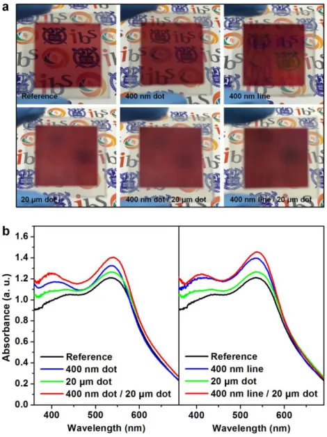
Then we investigated light harvesting characteristics of N719 dye- sensitized mp-TiO2 films, in order to ascertain the validity of our approach in state-of-the-art photoelectrode. Figure 2-8a shows the digital photographs of N719-sensitized flat and patterned mp-TiO2. Although the dye loading amounts are almost the same for both flat and patterned photoelectrodes (see Table 2-1), presence of 400 nm patterns resulted in darker coloration, indicating that more photons are trapped in nano- patterned photoelectrodes. In case of the micro-patterned mp-TiO2, randomized light scattering were observable from the significant drop in transparency which makes the background images completely undistinguishable. For a more detailed discussion on the light harvesting properties, absorbance spectra of dye-sensitized photoelectrodes were obtained in the visible light region, and the results are displayed in Figure 2-8b. By comparing the cases of flat, 400 nm dot, and 400 nm line patterned TiO2, significant enhancement in light absorption properties at low wavelength regions (< 550 nm) are observable in nano-patterned oxide films.
Also, superior light harvesting characteristic of 400 nm line patterns to that
increase of absorbance in longer wavelength range compared to the mp- TiO2 with 400 nm patterns. Most importantly, multilevel multiscale patterned mp-TiO2 exhibited largest absorbance in whole visible light region with superpositioned optical properties of nano- (diffraction grating) and micro-scale (randomized light scattering) architectures. Meanwhile, 400 nm line / 20 μm dot case was better than 400 nm dot / 20 μm dot, as could have been expected by the results from single-layer patterned photoelectrodes.
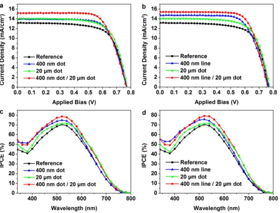
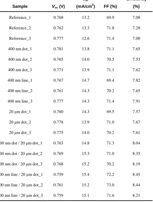
For the verification of the effectiveness of multilevel multiscale patterned mp-TiO2 photoelectrodes, DSSCs employing N719-sensitized TiO2, platinized FTO counter electrode, and I3-/I- redox electrolyte were prepared. Figure 2-9a and 8b show the photocurrent density (J)-voltage (V) characteristics of the DSSCs with various single- and multilevel patterned TiO2 films, and the detailed photovoltaic parameters are summarized in Table 2-2. Though differences in open-circuit voltage (Voc) and fill factor (FF) values were not significant (less than 3%), changes in short-circuit photocurrent density (Jsc) were varied with strong dependence on the types of patterns imprinted on mp-TiO2. Jsc increased as periodic structure of 400 nm dot, 400 nm line, or 20 μm dot was inserted on the mp-TiO2, from 13.0 mA/cm2 to 13.9 mA/cm2, 14.4 mA/cm2, or 14.1 mA/cm2, respectively. The degree of increments was much larger when multilevel multiscale structures were utilized, and the Jsc values exceeded 15 mA/cm2 in both 400 nm dot / 20 μm dot (15.1 mA/cm2) and 400 nm line / 20 μm dot (15.2 mA/cm2) cases.
Accordingly, the average conversion efficiencies of DSSCs with multilevel patterns were the highest, exhibiting 15.0% and 17.5% enhancements in 400 nm dot / 20 μm dot (8.19%) and 400 nm line / 20 μm dot (8.37%) patterned DSSCs compared to the reference (7.12%). Comparison between the efficiencies of DSSCs with single-level patterns and multilevel multiscale patterns clearly show that the multiple periodic architectures are effective strategies to enhance the overall performance of mesoscopic solar cells.
In order to confirm the origin of the enhancements in photocurrent densities and energy conversion efficiencies, IPCE measurements were performed. Figure 2-9c and Figure 2-9d show the IPCE spectra of DSSCs employing flat, single- and multilevel patterned mp-TiO2 photoanodes. The spectral characteristics of IPCE values were in accordance with the absorption results discussed above (Figure 2-8b). The 400 nm patterns induced more efficient photon utilization at relatively shorter wavelength lights, whether the periodic 20 μm dots exhibited enhancements in whole visible light region with comparative superiority to 400 nm in the harvesting of low energy (long wavelength) photons. From the observation of integrated improvements resulted from the constituent single-scale structures in multilevel multiscale mp-TiO2 based DSSCs, we could verify
Additionally, in order to demonstrate the general merits of our multiscale approach, we also prepared DSSCs with 800 nm dot, 800 nm line, 800 nm dot / 20 μm dot, and 800 nm line / 20 μm dot patterned mp-TiO2
photoanodes. As can be seen from the SEM images displayed in Figure 2- 10, the patterns were uniformly imprinted on the mp-TiO2 film by soft- molding, and full projection of nano- and micro-patterns by z-axis integration were observable in multilevel multiscale mp-TiO2. When these photoelectrodes were employed in DSSCs, significantly enhanced Jsc and energy conversion efficiencies with the similar trends to 400 nm / 20 μm cases were obtained, as can be seen from the J-V curves in Figure 2-11 and detailed summary in Table 2-3. DSSCs with 800 nm dot and 800 nm line patterned mp-TiO2 photoanodes showed enhanced Jsc and efficiency compared to the flat reference, and further increases were obtained by integration of 800 nm patterns with periodic 20 μm dots. Though the combination of 800 nm and 20 μm patterns were slightly inferior to multilevel 400 nm / 20 μm cases, general effectiveness of our multiscale z- axis integration strategy was confirmed.
Figure 2-8. (a) Digital photographs of flat and patterned mp-TiO2 with dye- sensitization. (b) Absorbance spectra of flat and patterned mp-TiO2 with
Figure 2-9. (a,b) J-V characteristics and (c,d) IPCE spectra of DSSCs employing mp-TiO2 with (a,c) flat, 400 nm dot, 20 μm dot, and 400 nm dot / 20 μm dot patterns and (b,d) flat, 400 nm line, 20 μm dot, and 400 nm line / 20 μm dot patterned structures.
Sample Voc (V)
Jsc
(mA/cm2) FF (%)
Efficiency (%)
Reference_1 0.768 13.2 69.9 7.08
Reference_2 0.762 13.3 71.8 7.28
Reference_3 0.777 12.6 71.4 7.00
400 nm dot_1 0.781 13.8 71.1 7.65
400 nm dot_2 0.765 14.0 70.5 7.53
400 nm dot_3 0.771 13.9 71.1 7.62
400 nm line_1 0.767 14.7 69.4 7.82
400 nm line_2 0.761 14.3 70.2 7.65
400 nm line_3 0.777 14.3 71.4 7.91
20 μm dot_1 0.760 14.3 69.5 7.57
20 μm dot_2 0.778 13.9 71.0 7.67
20 μm dot_3 0.775 14.0 70.2 7.61
400 nm dot / 20 μm dot_1 0.763 14.8 71.3 8.04
400 nm dot / 20 μm dot_2 0.769 15.3 71.0 8.35
400 nm dot / 20 μm dot_3 0.768 15.2 70.2 8.19
400 nm line / 20 μm dot_1 0.759 15.4 72.2 8.45 400 nm line / 20 μm dot_2 0.761 15.2 73.0 8.44 400 nm line / 20 μm dot_3 0.759 15.1 71.6 8.21
Table 2-2. Detailed J-V characteristics of the DSSCs employing flat or
Figure 2-10. Top-view SEM images of (a) 800 nm dot, (b) 800 nm line, (c) 800 nm dot / 20 μm dot, and (d) 800 nm line / 20 μm dot patterned mp-TiO2
films. The insets show enlarged images taken at higher magnifications.
Figure 2-11. J-V characteristics of DSSCs employing (a) 800 nm dot and 800 nm dot / 20 μm dot patterned photoelectrodes and (b) 800 nm line and
Sample
Dye-loading (× 10-7 mol/cm2)
Voc
(V)
Jsc
(mA/cm2) FF (%)
Efficiency (%)
800 nm dot 5.21 0.773 13.7 71.4 7.56
800 nm line 5.24 0.755 14.3 70.7 7.66
800 nm dot / 20 μm dot 5.33 0.763 14.8 71.1 8.03 800 nm line / 20 μm dot 5.27 0.756 15.0 71.2 8.09
Table 2-3. J-V characteristics of the DSSCs employing 800 nm dot, 800 nm line, 800 nm dot / 20 μm dot, or 800 nm line / 20 μm dot patterned mp-TiO2
photoelectrodes.
2-4. Summary
In this study, we performed investigations on photonic application of multilevel multiscale patterned nano-oxide photoelectrodes for efficient light harvesting in mesoscopic solar cells. By controlling the degrees of polymerization at the surface of UV-curable PUA membrane, monolithic integration of free-standing PUA membranes with nano- and micro-scale architectures were enabled by LEGO®-like multiplex lithography. Based on this technique, multilevel multiscale patterned PDMS film was replicated, and its structure was imprinted on mesoporous TiO2 film by soft-molding method. Formation of multilevel multiscale periodic structures on TiO2 nanoparticle photoelectrodes were directly observed by electron microscope analyses, and characteristic optical properties of the multiscale patterned nano-oxide electrodes were verified by keen experiments and simulations.
The z-axis integration of nano- and micro-patterns resulted in superposition of optical responses from nano- and micro-scale structures, enabling synergistic photon trapping within the photoelectrode by simultaneous diffraction grating and light scattering. Moreover, we confirmed the effectiveness of our approach by employing mp-TiO2 with multilevel 400
that our approach provides a convenient, reliable, and industrially favorable (repeatable fabrication even in a large dimension) method for enhanced light harvesting in mesoscopic solar cells, our multilevel multiscale patterning strategy for superposition of optical properties is anticipated to bring substantial advances and insights to the photoelectrode designs and architectures for maximization of light harvesting.
Chapter 3. Creep-assisted sequential imprinting method and its application to polymer electrolyte fuel cells
Published in ACS applied materials & interfaces, 2016, 8, 11459
3-1. Introduction
Multiscale hierarchical structures, the combined structures of micro- and nano-scale repeated pattern, have received great attention due to their structural advantages from individual micro- and nano-scale morphology simultaneously1-5. This synergetic effect of multiscale structures provides multifunctional properties to the raw material without any chemical treatment, which value of multiscale structures has been verified in various application fields such as microfluidics98-100, wetting and adhesion23, 101, optics102-104, electronics18-19, and energy systems20-21, 105. Therefore, many researchers have been trying to fabricate the multiscale structures covering large area in various processes. With conventional multiscale-patterning processes, however, introducing the nano-scale patterns on the top and bottom side of micro-patterns was only possible (not including the wall side