저작자표시-비영리-변경금지 2.0 대한민국 이용자는 아래의 조건을 따르는 경우에 한하여 자유롭게
l 이 저작물을 복제, 배포, 전송, 전시, 공연 및 방송할 수 있습니다. 다음과 같은 조건을 따라야 합니다:
l 귀하는, 이 저작물의 재이용이나 배포의 경우, 이 저작물에 적용된 이용허락조건 을 명확하게 나타내어야 합니다.
l 저작권자로부터 별도의 허가를 받으면 이러한 조건들은 적용되지 않습니다.
저작권법에 따른 이용자의 권리는 위의 내용에 의하여 영향을 받지 않습니다. 이것은 이용허락규약(Legal Code)을 이해하기 쉽게 요약한 것입니다.
Disclaimer
저작자표시. 귀하는 원저작자를 표시하여야 합니다.
비영리. 귀하는 이 저작물을 영리 목적으로 이용할 수 없습니다.
변경금지. 귀하는 이 저작물을 개작, 변형 또는 가공할 수 없습니다.
공학박사학위논문
아노다이징의 국부화 기술을 이용한 마이크로 산화알루미늄 패턴 가공
Micro Fabrication of Aluminum Oxide Patterns using Local Anodization
2015 년 8 월
서울대학교 대학원
기계항공공학부
지 원 영
Micro Fabrication of Aluminum Oxide Patterns using Local Anodization
DISSERTATION
SUBMITTED TO THE SCHOOL OF MECHANICAL
AND AEROSPACE ENGINEEERING AND THE COMMITTEE ON GRADUATE STUDIES OF SEOUL NATIONAL UNIVERSITY
IN PARTIAL FULFILLMENT OF THE REQUIREMENTS FOR THE DEGREE OF DOCTOR OF PHILOSOPHY
Won Young Jee
August 2015
Abstract
Won Young Jee School of Mechanical and Aerospace Engineering The Graduate School Seoul National University
In this study, the fabrication process of aluminum oxide pattern using local anodization was investigated. This process is known as local anodic oxidation (LAO) or scanning probe microscope (SPM) lithography for nano scale surface texturing [1]. However, an aluminum oxide formed by SPM anodization process has the ultimate thickness (the order of several tens of nm). Electrochemical machining (ECM), based on the electrochemical reactions between two electrodes, is a method for the machining of conductive materials. Micro ECM that uses ultra- short pulses allows localization of the electrochemical reaction to only a few micrometers of the surface due to the selective charging of a double layer. Therefore, using a principle of micro ECM, the aluminum oxide with micro scale depth can be
ii
localized. In the present study, mixtures of sulfuric/oxalic acid electrolyte was tested as feasible electrolytes for aluminum. Behavior of localized oxide growth was analyzed using by field emission scanning electron microscopy (FE-SEM) including energy dispersive spectroscopy (EDS) and it was confirmed that the number of micro-depth localized aluminum oxide was fabricated at specific location on aluminum surface. Depth and width of the anodized oxide line were investigated in different ratios of sulfuric and oxalic acid mixtures at various microsecond pulse duration and applied voltage condition. The insulation characteristics of fabricated aluminum oxide line were investigated and verified its possibility as an electric circuit. Subsequently, a coplanar waveguide (CPW) micro patch antenna was fabricated and characterized by a PNA network analyzer. The local anodization can be used for fabricating micro-electric circuits without masks and substrate; which will promise the next generation of micro electronic devices.
Keywords: Local anodization, Local anodic oxidation, Scanning probe microscope lithography, Micro electrochemical machining, aluminum oxide, RF antenna
Student number: 2008-22894
iii
Contents
Abstract ... i
Contents ... iii
List of Figures ... v
List of Tables ... ix
1. Introduction ... 1
1.1 Research background ... 1
1.2 Research objective and dissertation overview ... 4
2. Principle and experiments... 6
2.1 Principle of local anodization ... 6
2.1.1 The Mott-Cabrera model ... 7
2.1.2 Chemical reaction ... 12
2.1.3 Oxide growth of typical anodization ... 17
2.1.4 Electrochemical with short pulses ... 20
2.2 Experimental system ... 25
2.2.1 Positioning system ... 28
iv
2.2.2 Pulse generator ... 30
2.2.3 Fabrication of tool electrode ... 32
3. Characteristics in local anodization ... 34
3.1 Oxide growth ... 29
3.2 Gap between tool electrode and workpiece ... 51
3.3 Ratio and concentration of electrolyte ... 56
3.4 Pulse conditions ... 64
4. Fabrication of aluminum oxide pattern and application ... 70
4.1 Fabrication of aluminum oxide pattern ... 70
4.1.1 Local anodization conditions ... 70
4.1.2 Fabrication of aluminum oxide pattern ... 72
4.2 Fabrication of radio-frequency antenna ... 78
2.2.1 Introduction of RF patch antenna ... 78
2.2.2 Fabrication of coplanar waveguide patch antenna ... 81
2.2.3 Local anodization on the non-flat aluminum surface ... 92
5. conclusion ... 97
Reference ... 99
v
List of Figures
Fig. 2.1 The interface of the adjacent to the barrier layer [34].
Fig. 2.2 Current-time curve and schematic for a typical anodization Fig. 2.3 Double layer model[37]
Fig. 2.4 Difference of charging potentials [37]
Fig. 2. 5 Difference of charging potentials
Fig. 2.6 Schematic diagram of experimental system
Fig. 2.7 Schematic diagram of WEDM for fabrication of micro electrode Fig. 2.8 Fabricated tool electrodes: (a) schematic of tool electrode,
(b) fabricated 𝝓 40 m tool electrode
Fig. 3.1 Aluminum oxide formed by local anodization: (a) SEM image of aluminum oxide, top view, (b) 2D surface profile of section a-a’
Fig. 3.2 3D surface profile of the localized aluminum oxide
Fig. 3.3 SEM image of the cross section of localized aluminum oxide formed by local anodization
vi
Fig. 3.4 Analysis of the cross section of aluminum oxide: (a) Target space of the EDS analysis (b) EDS map data of the surface
Fig. 3.5 EDS profile of the cross section of aluminum oxide Fig. 3.6 FE-SEM images of the cross section of center of the oxide Fig. 3.7 The height of the oxide according to time
Fig. 3. 8 FE-SEM images of a cross section and surface of localized aluminum oxide (etched by FIB)
Fig. 3. 9 FE-SEM image of a cross section of a porous oxide layer Fig. 3. 10 BSE micrographs of cross section and dense oxide layer [42]
Fig. 3. 11 Load-depth curves of localized oxide by nano indentation test Fig. 3. 12 SEM image of oxide 15m inter-electrode gap at 20 V
Fig. 3. 13 Simulation results of Φc according to distance
Fig. 3. 14 Localized oxide surface according to time (a) 5 m gap, (b) 10 m gap Fig. 3.15 SEM image of the local anodization in 0.1 M H2SO4 electrolyte
Fig. 3.16 Anodized aluminum oxide line in different concentration of electrolyte (a) 0.1 M H2SO4, 20 V (b) 1 M H2SO4, 10 V
Fig. 3.17 Depth and width of the anodized oxide in different ratio of H2SO4/C2H2O4
acid mixtures
Fig. 3. 18 SEM images of cross section of the oxide line at 25 V (a) C2H2O4 (b) C2H2O4 + H2SO4 = 1:1 (c) 0.5 M H2SO4
Fig. 3.19 Pulse signal
vii
Fig. 3.20 Depth and width of the anodized oxide in different pulse on-time Fig. 3.21 Charging voltage according to pulse on-time
Fig.4.1 Exposure time of the point on the path line
Fig. 4.2 Micro oxide pattern by local anodization (ø 40 m electrode, 500 m thick Al sheet, 20 V, 500 ns pulse on-time, 5 s period)
Fig. 4.3 SEM images of the fabricated penetrating oxide line (top, bottom) Fig. 4.4 Optical image of penetrating oxide line by local anodization Fig.4.5 SEM images of aluminum oxide pattern. (a) top view
Fig. 4.6 Basic features of a patch and CPW patch antenna
Fig.4.7 The geometrical configuration of the CPW micro patch antenna on aluminum sheet.
Fig.4.8 The fabricated CPW patch antenna using local anodization and was attached on the SMA connector.
Fig.4.9 The absorbing performance of the fabricated CPW patch antenna
Fig.4. 10 The geometrical configurations of air-backed antenna and antenna on polyimid substrate
Fig.4. 11 The fabricated CPW patch antenna with polyimide substrates by LBM and was attached on the SMA connector
Fig.4. 12 Comparison of performance with reflection loss (S11) and bandwidth (-10 dB)
Fig.4.13 Local anodization process on the curved surface
viii
Fig.4.14 Schematic of the rotation system for local anodization on curved surface and image of fabrication
Fig.4.15 Optical and SEM image of aluminum oxide pattern on non-flat surface
List of Tables
Table 2.1 Specification of positioning system Table 2.2 Specifications of the pulse generator Table 3.1 Conditions of local anodization
Table 3. 2 Conditions and results of the nano-indentation Table 3.3 EDS analysis of area 1, 2 in Fi. 3.8 (b)
Table 3.4 Conditions of local anodization
Table 4.1 Conditions of local anodization for penetrating oxide line Table 4. 2 Conditions of laser beam machining process
Table 4.3 Conditions of local anodization for oxide pattern on curved surface
1
Chapter1
Introduction
1.1 Research background
Anodic oxidation or anodizing is an electrolytic process for producing thick oxide coatings that can improve physical and chemical properties for application of aluminum [2]. The anodic oxide coating also provide abrasion resistance, an electrical insulation, and absorbing dyestuffs to give a wide range of colors [1, 3].
Therefore, anodic oxide films on aluminum have been investigated for improving its electrical/chemical corrosion resistance and decorative coating [4-6]. Many studies show that various electrolyte of acid or acid mixtures can be used for their purposes. The most widely used anodizing specification is a U.S. military spec.
MIL-A-9625, which defines three types of aluminum anodization. (Type Ⅰ-
2
chromic acid, Type Ⅱ & Ⅲ- sulfuric acid) [7]. Other electrolytes are organic acid (such as oxalic acid, malic acid, etc.), phosphoric acid, and so on [1, 2].
As the market demands changes that require micro technologies in electronics industry and electrical circuits became extremely compact,[8] various attempts have been made to use dielectric characteristics of anodic aluminum oxide in the fabrication of micro-electric components and micro-engineered structures. Kikuchi et al. introduced electrochemical etching/deposition techniques with the combination of anodizing and laser irradiation [9-11]. Aluminum specimens covered with porous type anodic oxide films were irradiated with a pulsed Nd-YAG laser to remove the oxide films locally, and then electrochemical etching or deposition were carried out on the exposed local aluminum surface. In their studies, aluminum oxide films were used for electrochemical etching/deposition mask, and were removed after the process.
The self-organized nanopore structures have also attracted attention due to their high pore density and their potential use for masking or micro sensors for electronic industry [12-15]. In the present studies, self-organized hexagonal arrays of uniform parallel nanopores (Anodic Aluminum Oxide, AAO) was used for various
3
applications in the fields of sensing, storage, separation, and the synthesis of one- dimensional nanostructures [16-19].
The concept of local anodization began with scanning probe microscopes (SPM) or atomic force microscope (AFM) [20, 21]. There have been many reports on the use of this technique to produce nanoscale patterns and transfer them into underlying material. In this technique, a voltage is applied between the conductive tip and the material’s surface, resulting in the formation of a narrow oxide line along the path followed or dot array by the advantage of precise control of local insulator fabrication. Meanwhile, an aluminum oxide formed by SPM anodization process has the ultimate thickness, the order of several tens of nm. If the thickness of oxide films are increased to micro scale, local aluminum oxide can be used for dielectric material of hard-to-make micro devices. In GHz radio frequency antenna engineering, for example, helical antenna structures that have high performance (bandwidth radiation efficiency, radiation resistance and optical transmission coefficient) than 2D structures are difficult to make [22]. The LIGA process, the most commonly used to make micro patch antenna, is limited to the fabrication of 2D micro structures with high aspect ratio [23-27]. Micro milling, micro EDM (electrical discharge machining), micro ECM (electrochemical machining) and LBM (laser beam machining) can be applied to machine micro structures with high
4
precision. However, these are all cutting process thus micro helical structure of antenna materials like copper or aluminum have robustness problem with maintaining its shape. Unfortunately, any other dielectric substance than air inside the helical structure to support decrease the antenna performance [22].
In this case, local anodization can be applied. Penetrating localized oxide of aluminum sheet may acts a dielectric space of helical strip and support the entire structure. Park et al. propose the local anodization process with photoresist mask patterns on aluminum surface to fabricate localized alumina line [28]. Yet, there is also a limitation on applying at non-flat surface. To apply the local anodization technique to micro manufacturing, further studies on increasing the depth of localized oxide on flat and non-flat surfaces are required.
1.2 Research objective and dissertation overview
In this dissertation, by using a principle of micro ECM, local anodization process to form the aluminum oxide with micro scale depth was investigated. Mixtures of sulfuric/oxalic acid electrolyte was tested as feasible electrolytes for aluminum.
Behavior of localized oxide growth was analyzed using by field emission scanning
5
electron microscopy (FE-SEM) including energy dispersive spectroscopy (EDS) and it was confirmed that the number of micro-depth localized aluminum oxide was fabricated at specific location on aluminum surface. Depth and width of the anodized oxide line were investigated in different ratios of 0.5 M sulfuric and 0.5 M oxalic acid mixtures at various microsecond pulse duration and applied voltage condition. The insulation characteristics of fabricated aluminum oxide line were investigated and application of local anodization is also introduced.
In chapter 2, the principal of local anodizing based on the Mott-Cabrera model and chemical reaction are presented. Description of experimental system is also presented.
In chapter 3, the oxide growth and the characteristics of the local anodization are presented. The effects of electrolytes, pulse conditions, and gap between tool and workpiece are analyzed.
In chapter 4, the fabrication of aluminum oxide pattern and micro patch antenna by local anodization is presented. The performance of the fabricated patch antenna was measured. Furthermore, local anodization is applied to non-flat cylindrical surface. As a result, possibility of using on fabrication of 3D micro electric circuit
Conclusion of this dissertation and discussion were presented in chapter 5.
6
Chapter 2
Principle and experiments
2.1 Principle of local anodization
Since the initial demonstration of surface anodization of semiconductors with SPM or AFM technology [21], there have been many reports about the physical mechanism and its relevance to anodization thickness and linewidth [20]. Actually, the oxide growth on metal surface starts out quickly but virtually stops after and oxide of finite thickness has been formed. The formation of this native oxide can be explained within the framework of the theory originally developed by Nevill Mott and Nicolas Cabrera [29, 30]. The additional oxide thickness ca be attributed to the field assisted Mott-Cabrera mechanism [31]. Although this theory explain the nano-scale phenomenon, it will be reasonable to understand mechanism of local anodization.
7
2.1.1 The Mott-Cabrera model
This model is discussed by follow the usual conventions[31, 32] and assume a quasi-one-dimensional system consisting of:
1. The parent material, i.e., bulk metal or semiconductor, for 𝑥 ∈ (−∞, 0) 2. An oxide layer of thickness X in the region 𝑥 ∈ (0, 𝑋)
3. A source of oxygen, e.g., air or water, for 𝑥 ∈ (𝑋, ∞)
After the formation of initial oxide layer, ions or ionic defects or neutral atoms should be transported through this film. In the steady state approximation, the concentration ns of each diffusing species s is assumed to be constant in time.
Particle conservation, in the form of the continuity equation ∂ns/∂t = ∂js/∂x, then dictates that ∂js/∂x = 0 and the particle current js is constant throughout the oxide.
Accordingly, the oxide growth rate can be wrote as 𝑑𝑋
𝑑𝑡
= ∑ 𝛺
𝑠 𝑠𝑗
𝑠 (2.1) where 𝛺𝑠 is the volume of oxide formed by the transversal of a single ion of species s [32].8
In general, the growth of oxide films is controlled by diffusion of ions and electrons under the influence of gradients of their concentrations and self-generated electric potential.: The contribution Vρ to the potential due to the space charge ρ (x) = ∑ 𝑞𝑠 𝑠𝑛𝑠(𝑥), where qs is the charge of a single ion of species s, can be found from Poisson’s equation and evaluates to (1 2𝜀⁄ )𝑋2𝜌 if 𝜌 is independent of x; if X ≪ √𝜀𝑘𝐵⁄𝑒𝜌, 𝑒𝑉𝜌 is small compared with 𝑘𝐵𝑇. [31].
By mott-cabrera assumption, electrons are transported through thin oxide films via tunneling or thermal emission and the electronic motion is rapid compared to the ionic motion. If a layer of oxygen is present at X, some of the oxygen atoms will be converted to O−ions until the chemical potential is equal on both sides of the oxide.
This charge separation causes a built-in voltage 𝑉𝑀 across the oxide, which is sometimes designated the Mott potential [31]. The magnitude of 𝑉𝑀 may be estimated by 𝑒𝑉𝑀 ≈ 𝐸𝐴𝑂+ 𝑊 − 𝜑𝑚, where 𝐸𝐴𝑂 is the electron affinity of oxygen, 𝑊 the binding energy of the oxygen ion, and 𝜑𝑚 the work function of the parent material; 𝑉𝑀 is typically of the order 1V.
For thin films, the electric field E = 𝑉𝑀⁄𝑋 becomes large and controls the ionic transport. If the particle current 𝑗𝑠 of ions of species s obeys the linear relation
9
𝑗𝑠 = 𝜇𝑠𝐸, where 𝜇𝑠 is the mobility, the assumption of single carrier transport leads to a growth rate [31, 32]
𝑑𝑋
𝑑𝑡
=
Ω𝜇𝑉𝑀𝑋 (2.2) which can be integrated to give the well-known parabolic law [29, 30]
𝑋(𝑡) ∝ √𝑡 − 𝑡0 (2.3)
which constant of proportionality √2Ω𝜇𝑉𝑀.
For very thin oxide layers, however, the electric field becomes so strong that 𝑗𝑠 is no longer proportional to E. In this case, the relationship between the electric field and the particle current can be derived from the hopping model originally formulated by Verwey [30, 33]: Let the distance between adjacent potential minima in the oxide be a and the energy barrier between them U. The classical Boltzmann probability that a particle will move from one site to the next is than ν exp (−𝑘𝑈
𝐵𝑇), where the attempt frequency ν can be identified with the typical phonon frequency [30, 33].An electric field E(x) lowers the activation energy barrier for movement in the positive x-direction by 12𝑎𝑞𝑠𝐸(𝑥). The hopping probability thus becomes ν exp [− {𝑈 −12𝑎𝑞𝑠𝐸(𝑥)} /𝑘𝐵𝑇] in the forward direction, while the probability for
10
hopping in the reverse direction is reduced to ν exp [− {𝑈 +12𝑎𝑞𝑠𝐸(𝑥)} /𝑘𝐵𝑇]
and can be neglected in the strong field limit 𝑎𝑞𝑠𝐸(𝑥) ≫ 𝑘𝐵𝑇. The particle current of species s is therefore given by
𝑗
𝑠≈
𝑛𝑠𝑎(𝑥)𝜈 exp (
𝑘−𝑈𝐵𝑇
) 2 sinh [
1
2𝑎𝑞𝑠𝐸(𝑥)
𝑘𝐵𝑇
]
. (2.4)In the strong field limit, 12𝑎𝑞𝑠𝐸(𝑥) ≫ 𝑘𝐵𝑇 and 2 sinh [12𝑎𝑞𝑠𝐸(𝑥) 𝑘⁄ 𝐵𝑇] can be approximated by exp [12𝑎𝑞𝑠𝐸(𝑥) 𝑘⁄ 𝐵𝑇] . Assuming that space charges are negligible, 𝐸(𝑥) = 𝑉𝑀⁄𝑋, 𝑛𝑠(𝑥) = 𝑛𝑠(0) and Eq. (2.4) becomes
𝑗
𝑠≈
𝑛𝑠(0)𝑎
𝜈 exp (
−𝑈𝑘𝐵𝑇
) exp [
1 2𝑎𝑞𝑠
𝑘𝐵𝑇 𝑉𝑀
𝑋
]
(2.5)For single carrier transport, Eqs. (2.1) and (2.5) imply
𝑑𝑋
𝑑𝑡
≈ Ω
𝑛(0)𝑎
𝜈 exp (
−𝑈𝑘𝐵𝑇
) exp [
1 2𝑎𝑞 𝑘𝐵𝑇
𝑉𝑀
𝑋
]
(2.6)If transport through the oxide is rate determining, n(0)is approximately independent of the oxide film thickness and determined by interfacial equilibrium conditions [33]. In contrast, if we follow Mott and Cabrera in assuming that the
11
transport in the presence of a strong field is very rapid and the limiting step is the dissolution of the ions at the interface, the rate of oxidation is given by
𝑑𝑋
𝑑𝑡
≈ Ω𝑁′𝜈 exp (−
𝑊𝑘𝑖+𝑈𝐵𝑇
) exp [
1 2𝑎𝑞 𝑘𝐵𝑇
𝑉𝑀
𝑋
]
(2.7) Where 𝑊𝑖 is the heat of solution of the ion, b the width of the energetic barrier it has to overcome, and N’ is the sheet density of ions available for dissolution [30].The derivation is analogous to the argument given above.
In both cases, dX/dt has the same functional form
𝑑𝑋
𝑑𝑡
= 𝑢
0exp (
𝑘−𝑊𝐵𝑇
) (
𝑋𝑋0)
(2.8)By considering growth to have stopped once𝑑𝑋/𝑑𝑡 ≳ 𝑢𝐿, a limiting oxide thickness XL can be defined as
𝑋
𝐿=
𝑋0𝑊 𝑘⁄ 𝐵𝑇−ln(𝑢0⁄𝑢𝐿)
(2.9) Following this conclusion, the oxide growth will stop at a thickness XL ∝X0∝VM
provided that 𝑊 [𝑘⁄ 𝐵𝑇 − ln(𝑢0⁄𝑢𝐿)], in agreement with the observed behavior of many metals [30].
12
The Mott–Cabrera-model is also applicable to the anodic formation of oxide films in an electrolyte [30] and LAO was originally explained as a straightforward extension to it. In the vicinity of the probe, the applied bias would lead to a larger voltage V dropped across the oxide. The oxide growth would terminate at a larger final oxide thickness XL in the affected areas [21].
2.1.2 Chemical reaction
The two main reactions of the formation of the porous oxide layer are (2.10) and (2.11). Reaction (2.10) shows the formation of aluminum oxide and reaction (2.11) the chemical dissolution of the oxide layer in an acidic electrolyte, such as sulfuric acid.
2Al + 3H2O → Al2O3 + 6H+ + 6e- (2.10) Al2O3 + 6H+ → 2A3+ + 3H2O (2.11) Beside reaction (2.11), another dissolution process must exist. When the rate of oxide growth is almost twice as high for a current, the chemical dissolution should double as it should to keep a steady state for formation and dissolution. This process is called the field-assisted dissolution. The field-assisted dissolution is a result of concentration of the field across the barrier layer. It causes concentration of the
13
current and thermally enhanced through local Joule’s heating [1]. This thermal energy weaken the Al-O bonds in the oxide lattice and cause a dissolution at the film/electrolyte interface. Between these two dissolution mechanisms, the chemical dissolution is much slower than the field-assisted dissolution [1].
The most important factor in aluminum anodizing is the behavior of the barrier layer. The electrical field across the barrier layer controls the dissolution rate of the oxide layer. In this regard, reaction (2.10) is purely field assisted process. The electrical field is the main reason for the possibility of the ions to move through the barrier layer at all. Many considerations have been done to explain this formation process of aluminum oxide.
Aluminum has the face centered cubic (fcc) crystal lattice. When Al3+ ions leave this metal lattice vacancies are formed. These vacancies provide room for the ingress of oxygen ions from the adjacent oxide layer to continue the formation of aluminum oxide. Due to the very small radius of Al3+, the ion can diffuse through the barrier layer under the influence of the electrical field easily present.the continued growth of the film is possible which makes The radius of Al3+ is 0.5 Å and that of O2- is in the order of 1.3 Å . The size of the oxygen ions makes the movement of these ions possible only when there is sufficient space8. Hoar and Mott9 suggested that the oxygen is transported not as O2- but as OH- which is much
14
smaller. The H+ ions found in the electrolyte may lead to the production of a hydroxyl ion instead of the oxygen ion according to reaction (2.12).
O2- + H+ ↔ OH- (2.12) Under the influence of the high field, the hydroxide ions will move through the oxide to the interface metal/barrier layer. It will react with Al3+, which is formed here and form aluminum oxide. If the oxide is formed by the hydroxide rather than the oxygen ions positive hydrogen ions will move back through the film and into the electrolyte. This means that the continuous formation of oxide (2.10) is dependent on the ability of migration of aluminum and oxygen ions through the barrier layer as shown in Fig. 2.1. Takahashi et al. [34] show the migration of oxygen ions through the barrier layer into the interface area metal/barrier layer where the reaction takes place. They do not take into considerations if the oxygen ion is too big to migrate through the aluminum oxide lattice. They also postulate that chemical dissolution, reaction (2.11), will take place at the interface barrier layer/electrolyte at a rate keeping the thickness of the barrier layer constant as determined by the applied voltage [34].
15
Fig. 2.1 The interface of the adjacent to the barrier layer [34].
16
2.1.3 Oxide growth of typical anodization
Investigations by a group at UMIST [1] give a explanation of the formation of porous oxide. They conclude that in all cases of film growth examined, Al3+ and O2-/OH- are mobile; the latter always develops solid film at the interface between metal and film whereas the contribution of out wardly mobile AL3+ ions to film formation depends upon the specific conditions of anodic polarization.
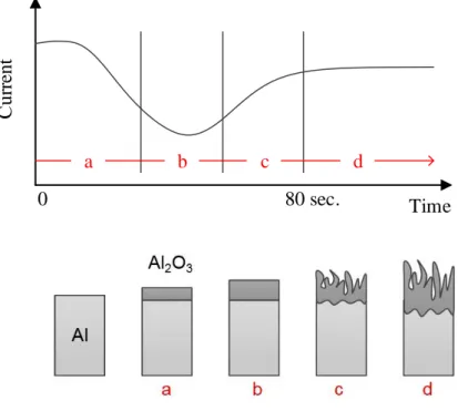
The initial stages of oxide growth correspond to a relatively uniform oxide thickness but by the egress of aluminum ions into the electrolyte penetrations paths will develop in top of the barrier layer. Between these penetration paths there will be a decrease in field strength and hence a decrease in the field assisted dissolution rate. As a consequence of these variations in the field strength the interface of aluminum and barrier layer will adopt the form of a fine scalloped structure. By concentration in the barrier layer of the electric field and the ionic current, beneath the major pores, a steady state porous anodic film is formed. The current - time curve obtained during the first 100 seconds of the anodizing will be as shown in Fig. 2.2. Here the process is performed with constant voltage during the anodizing process.
17
Time
Current
0 80 sec.
a b c d
Fig. 2.2 Current-time curve and schematic for a typical anodization
18
Period a in Fig. 2.2 shows the formation of the first microns of oxide. In the beginning the current is high due to the fact that the current only passes through the metallic aluminum. Then the current starts to decrease because of the formation of a thin non-porous oxide layer. This oxide layer has a higher resistance than the metallic aluminum. The increase in thickness and therefore an increasing resistance result in a further decrease in the current in period b. The tendency of the curve to turn upwards in period b is due to small imperfections (roughness) in the compact oxide layer. These small imperfections are formed by the concentration of the current in areas with thinner oxide than on the rest of the surface. According to Keller et al. [35] these areas with the small imperfection are the subgrain boundaries found on aluminum. They stated that these areas are the places where the initial formation of cells starts. The natural oxide film on either side of these subgrain boundaries is not as compact or uniform as on the rest of the surface. Therefore these areas offer less resistance to the current. Considering the formation of a single cell of oxide. At a single point the dissolution reaction is started, hence the oxide thickness is reduced and the current will start to flow to repair the damage. This will increase the temperature of the electrolyte and the solution will be more reactive and thus increase the rate of dissolution. This mechanism will perpetuate a
19
pore once formed. According to Keller et al. [35] this mechanism could be halted.
Therefore some pores will perpetuate and others will never get started. Hence the current will concentrate on these small imperfections. This will increase the electrolyte temperature in these areas. Therefore the dissolution will increase and the oxide layer will become even thinner. The current will increase as seen in period c in Fig 2.2. Now the formation of the porous oxide layer has started. In period d the current will reach a constant level where the rates of dissolution and formation of the oxide layer reach a steady state level.
2.1.4 Electrochemical cell with short pulses
During the anodization, when the initial oxide layer (barrier layer) has formed, enough mass cannot pass through the layer for the continuous oxide growth. To form thick oxide layer, increase the rate of field-assisted dissolution through barrier layer using high voltage. Therefore, high and local electrical field should be restricted to the target region to localize the oxide. Localized anodizing uses principle of micro ECM, which uses very close to the electrode end to workpiece and localize the electrochemical reaction region by the ultra-short pulse voltage [36].
20 Tool
electrode
Workpiece Cd
Rs, small
Rp
Rs, large
Fig. 2.3 Double layer model[37]
21
The electrochemical cell with two electrodes of tool and workpiece is illustrated as an equivalent RC circuit in Fig. 2.3 which consists of double layer capacitances Cd, polarization resistances Rp and electrolyte resistance Rs. When ultrashort pulse is applied between two electrodes, it is allowable to take into consideration only transient response. Hence, the polarization resistance can be neglected, so that the equivalent circuit can be simplified into the RC circuit with Cd and Rs. the electrolyte resistance is proportional to the gap distance d. In the region where the distance between electrodes is small, the resistance of electrolyte per unit area, Rs
is:
R𝑠,𝑠𝑚𝑎𝑙𝑙 = 𝜌𝑑𝑠𝑚𝑎𝑙𝑙 (2.13) where 𝜌 is the specific electrolyte resistance. Where the distance is large, Rs is:
R𝑠,𝑙𝑎𝑟𝑔𝑒 = 𝜌𝑑𝑙𝑎𝑟𝑔𝑒 (2.14) The charging time constant τ of the double layer in each region can be expressed as:
𝜏
𝑠𝑚𝑎𝑙𝑙=
12𝑅
𝑠,𝑠𝑚𝑎𝑙𝑙𝐶
𝑑=
12𝜌𝐶
𝑑𝑑
𝑠𝑚𝑎𝑙𝑙 (2.15)𝜏
𝑙𝑎𝑟𝑔𝑒=
12𝑅
𝑠,𝑙𝑎𝑟𝑔𝑒𝐶
𝑑=
12𝜌𝐶
𝑑𝑑
𝑙𝑎𝑟𝑔𝑒 (2.16)22
From these equations, the charging time for the double layer is proportional to the inter-electrode gap. In the small gap 𝑑𝑠𝑚𝑎𝑙𝑙, the charging time is shorter than in the large gap 𝑑𝑙𝑎𝑟𝑔𝑒. When pulses with the on-time T (𝜏𝑠𝑚𝑎𝑙𝑙 ≤ 𝑇 ≤ 𝜏𝑙𝑎𝑟𝑔𝑒) are applied between electrodes, the double layer only in the small gap is charged over the effective potential Φ𝑒𝑓𝑓, which is sufficient over-potential for reaction. The double layer potential where the inter-electrode gap is large does not reach the effective potential due to its long charging time, as shown in Fig.2.4 and Fig. 2.5.
Since the chemical reaction rate is exponentially proportional to the potential of the double layer, the reaction can be restricted to the region very close to the electrode.
This ECM model is feasible at each frequency range of applied electric source.
23 Time
Potential
0 T
Φpulse (t)
Φ1 (t)
Φ2 (t)
τ smalll = R1 s,small Cd
2
τ large = R1 s,large Cd
2
Fig. 2.4 Difference of charging potentials [37]
Fig. 2. 5 Difference of charging potentials
24
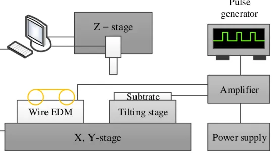
2.2 Experimental system
As shown in Fig.2.6, the experimental system consists of the wire electrical discharge machining (WEDM) system and local anodizing system. Two systems were attached to the same three-axis stage with a resolution of 0.1 m to avoid tool runout. The local anodization system was made up of an electrochemical bath, pulse generator, amplifier, power supply, and tilting stage. A micro cylindrical tungsten carbide (WC) shaft was used as the tool electrode (cathode) and installed on the spindle motor. Since this material is possible to make a straight electrode with a high aspect ratio at the micro scale [38]. The WC shaft with 300 m in diameter was fabricated by WEDM to obtain a micro electrode with a final diameter (20, 40, 100 m) and insulated with enamel except for the bottom surface to concentrate the current. Pulses between an electrode and a workpiece were measured by an oscilloscope. As a workpiece, highly pure (99.999 %, Nilaco Co.) aluminum was used and cleaned in C2H5OH solution and anodized in H2SO4 + C2H2O4 solution at room temperature(293 K), with a micro second pulse voltage. The tool electrode was scanned above the workpiece retaining a certain distance between electrode
25
tool and workpiece. In this experiment, X-Y stage and Z stage were used for the three dimensional positioning.
26
Z – stage
Wire EDM
Subtrate Tilting stage
X, Y-stage
Amplifier
Power supply Pulse generator
Fig. 2.6 Schematic diagram of experimental system
27
2.2.1 Positioning system
Since the anodiziation process is carried on with a very small gap, precise movement and certain inter-electrode gap are important. Hence, the electrode feed should be controlled with micro-meters accuracy. In this research, the X-Y stage is 315082AT stage of Parker Automation. The X-Y stage on which an anodization and WEDM bath were mounted was used to move a workpiece horizontally. The Z stage (4042200XR stage, Parker Automation) control the gap between micro tool and workpiece vertically. Both stages controlled by stepping motors (ZETA57-83, Parker Automation). Linear encoders were attached to control the position with resolution of 0.1 m /count. All systems were controlled by CEM-Clipper (Delta Tau Data Systems, Inc.) and monitored by PC. The specifications of the stages are shown in table 2.1.
28
X-Y stage Z stage
Model 325082AT
Parker Automation
404200XR
Parker Automation
Motor ZETA 57-83 stepping
motor
ZETA 57-83 stepping motor
Travel 200 mm, respectively 200 mm
Positional repeatability
1.3m 1.3m
Resolution 0.1 m /count 0.1 m /count Limit/home
switch
Optical sensor type Optical sensor type Table 2.1 Specification of positioning system
29
2.2.2 Pulse generator
A pulse generator played a role to provide a potential difference between workpiece and tool electrodes. To apply several microsecond pulses, 8551 (Tabor Electronics), of which rising time is minimum 8ns, was used. Generally in the high frequency circuit, input/output impedance are set to be 50 ohms to reduce transmission loss and signal shape distortion. The output impedance of this pulse generator is 50 ohms as well. However the impedance of the electrochemical cell is hard to define, because the electrolyte resistance and the double layer capacitance are varied according to the cell configurations. To minimize the effect of impedance mismatch, a unity gain voltage follower circuit without resistors was connected.
30
Model 8551, Tabor Electronics
Amplitude -8 ~ 8V
Pulse width 10 ns ~ 999 ms
Pulse repetition frequency ~ 50 MHz
Rise and fall time Tr ≤ 6ns, Tf ≤ 6 ns
DC offset -8 ~ 8 V
Output impedance 50 Ω
Table 2.2 Specifications of the pulse generator
31
2.2.3 Fabrication of tool electrode
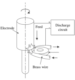
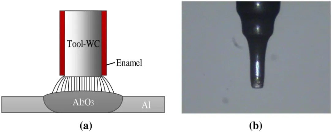
To fabricate micro aluminum oxide pattern, tool electrodes should be precisely machined. As a technique to fabricate micro electrodes, wire EDM (WEDM) was employed, which is used to machine electrically conductive materials such as steel, graphite, silicon and magnetic materials in the simple way [39]. WEDM is applied for the machining of micro electrode which has uniform diameter as shown in Fig.
2.7. A wire is fed along the wire guide, so the tool wear is negligible [40]. Using this method, a micro electrode of tens of micro meter in diameter can be fabricated within 3 m errors. The WC shaft with 300 m in diameter was fabricated by WEDG to obtain a micro electrode with a final diameter (20, 40, 60 m) and insulated with enamel except for the bottom surface to concentrate the current as shown in Fig. 2.8 (a). The fabricated tool electrode is shown in Fig. 2.8 (b).
32
Discharge circuit +
Electrode Feed -
Brass wire
Fig. 2.7 Schematic diagram of WEDM for fabrication of micro electrode
AlAl2O3
Tool-WC
Enamel
(a) (b)
Fig. 2.8 Fabricated tool electrodes: (a) schematic of tool electrode, (b) fabricated 𝝓 40 m tool electrode
33
Chapter 3
Characteristics in local anodization
3.1 Oxide growth
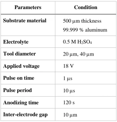
The local anodization was carried out at one point on the aluminum surface using 20 m diameter tool electrode and confirmed creation of oxide. Fabricated oxide was analyzed by the field-emission SEM including energy dispersive spectroscopy (AURIGA FE-SEM, Carl Zeiss). To minimize local shortage of ions and supply fresh electrolyte, tool electrode was rotated at 240 rpm. The tool electrode moved down from a height of standby position to anodizing position for 2 min. Detail experimental conditions are determined by the parameters as shown in Table. 3.1.
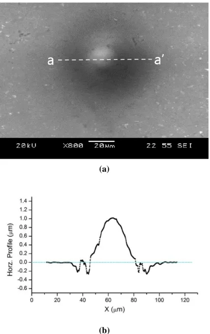
Fig. 3.1 shows the SEM and 2D surface profile (a-a’) images of dome-shaped aluminum oxide. The anodized area is about 40 m in diameter and 1 m higher than the height of the substrate surface. It means a local area of the aluminum is sufficiently anodized.
34
Parameters Condition
Substrate material 500 m thickness 99.999 % aluminum
Electrolyte 0.5 M H2SO4
Tool diameter 20 m, 40 m
Applied voltage 18 V
Pulse on time 1 s
Pulse period 10 s
Anodizing time 120 s
Inter-electrode gap 10 m
Table 3.1 Conditions of local anodization
35 (a)
(b)
Fig. 3.1 Aluminum oxide formed by local anodization: (a) SEM image of aluminum oxide, top view, (b) 2D surface profile of section a-a’
36
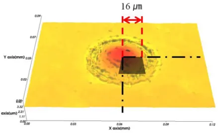
Fig. 3.2 3D surface profile of the localized aluminum oxide
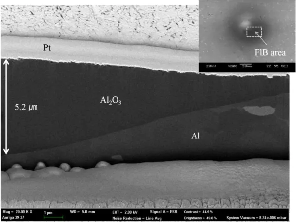
To observe the inside, the right half cross section of the symmetrical oxide was etched by Focused Ion Beam (FIB, AURIGA, Carl Zeiss) after sputtering the platinum to protect the surface from FIB (Fig. 3.2). As shown in Fig. 3.3, aluminum oxide was formed with about 5.2 m depth and interfacial line between oxide (dark area) and aluminum (lighter area) layer is clearly distinguished. The curve of the interfacial line indicate an electric field level caused by electrode and workpiece.
Fig. 3.4 shows the energy dispersive spectroscopy (EDS) and profile images of the oxide in Fig. 3.3. EDS spectra profile analysis provides the elemental
37
composition maps of materials. EDS spectra of aluminum (green) and aluminum oxide (red) where the oxygen peak appears (Fig. 3.4(b)). As a result, it is confirmed that the number of micro-depth localized aluminum oxide was fabricated at specific location on aluminum surface using a micro electrode tool.
Fig. 3.3 SEM image of the cross section of localized aluminum oxide formed by local anodization
38 (a)
(b)
Fig. 3.4 Analysis of the cross section of aluminum oxide: (a) Target space of the EDS analysis (b) EDS map data of the surface
39
Fig. 3.5 EDS profile of the cross section of aluminum oxide
40 Formation of the oxide layer
As discussed in chapter 2.1.2, the two main reactions of the formation of the oxide layer are formation of aluminum oxide, and the chemical/electrical dissolution of the oxide layer. Fig. 3.6 and Fig. 3.7 were obtained during the first 120 seconds of the anodization which shows that oxide growth and main reactions according to time. The images in Fig. 3.6 are the cross sections located at center of the oxide and etched by FIB (AURIGA, Carl Zeiss). For better observation of the oxide growth, lager 40 m diameter tool was used.
Period 0 ~ 30 s in Fig. 3.6 (a) shows that the formation of the first microns of oxide and chemical/electrical dissolution and formation are occurred. Accordingly, height of the oxide become lower than substrate surface. Then the current starts to decrease because of the formation of a thin barrier layer. This oxide layer has a higher resistance than the metallic aluminum. During the period 30~60 s, small imperfections are formed by the concentration of the current in areas with thinner oxide due to higher field assistant dissolution [35]. As shown in Fig. 3.7 (b), overall thickness of the oxide is maintained with about 1.8 m during 30 ~ 60 s. The imperfections stated that these areas are the places where the initial formation of pores starts. Then, while the oxide thickness is reduced, the height of overall porous
41
oxide is increased and the current will start to flow to repair the damage, 60~90 s [35]. Then, during the 90 ~ 120 s, A thick oxide layer raise the temperature of electrolyte around the barrier layer and it will lead to an increase in the rate of chemical dissolution. The depth of the barrier layer has reached a level where the field strength has increased enough and suddenly the current increases steeply [35].
It makes local crack on the barrier and electrical/chemical dissolutions are occurred again. As a result, depth of the oxide is deepen continuously.
42
(a) 30 s (b) 60 s
(c) 90 s (d) 120 s
Fig. 3.6 FE-SEM images of the cross section of center of the oxide
43
(a) 2D surface profile of the oxide: 30 s, 60 s, 90 s, 120 s.
(b) Height of the oxide surface and depth Fig. 3.7 The height of the oxide according to time
44 Structure of the oxide layer
Observing the cross section of the fabricated oxide layer, the porous structure is not visible as shown in Fig. 8. That is dense oxide structure as seen in the hard anodizing [7]. Hard anodizing or hard coat are known as anodizing Type III, which enables aluminum surface to have thick oxide layer. Anodizing thickness increases wear resistance, corrosion resistance, ability to retain lubricants, and thermal/electrical insulation. During the hard anodizing, a uniform aluminum oxide layer is formed on the surface that penetrates into the material in sulfuric acid alone or with additives. The acid and the applied electric field condition in local anodization is similar to hard anodizing condition, thus dense aluminum oxide can formed. When compared to previous studies, as shown in Fig. 3.9 (pore oxide) and Fig. 3.10 (dense oxide), it is certain that the oxide layer fabricated by local anodization is that of hard anodizing.
45
Fig. 3. 8 FE-SEM images of a cross section and surface of localized aluminum oxide (etched by FIB)
46
Fig. 3. 9 FE-SEM image of a cross section of a porous oxide layer (near the surface) [41]
Fig. 3. 10BSE micrographs of cross section and dense oxide layer [42]
47 Hardness of the oxide layer
Fabricated oxide layer can act as not only an electric insulator but also a supporting of the electric circuit structure. Thus the mechanical characteristic of aluminum oxide was measured with indentation hardness test. Indentation is the most commonly applied means of testing the mechanical properties of materials. The nano-indentation technique was developed to measure the hardness of small volumes of material. The maximum loading depth cannot be more than 10 % of the sample thickness, tested depth was 150 nm, because the thickness of oxide layer are 2~10 m. Berkovich diamond tip was used for indenter and sample the data from the 6 points of the oxide surface. Detail experimental conditions are determined as shown in table 3. 2. The load depth curves results is shown in Fig. 3. 11. From extracting 6 sample data, 7.295 GPa and 109.96 GPa were gained for mean indention hardness (HIT) and mean indentation modulus. Generally, oxide in hard anodizing condition have 3 to 10 GPa hardness and 90 to 200 GPa modulus. As a results, the oxide layer fabricated by local anodization can support circuit structure and provides higher stiffness.
48
Fig. 3. 11 Load-depth curves of localized oxide by nano indentation test
49
Test condition and results
Indenter Berkovich diamond tip
Loading Linear loading
Max. depth 150 nm
Applied voltage 1 m/min
Sampling data 6 point
HIT (Indentation hardness, Mean) 7.295 GPa EIT (Indentation modulus, Mean) 109.96 GPa
Table 3. 2 Conditions and results of the nano-indentation
50
3.2 Gap between tool electrode and workpiece
Theoretically, in ECM, shorter gap between tool electrode and workpiece has advantage of localizing reaction. However, electrolyte should be filled between electrodes and generated bubble during chemical reaction prohibit next chemical reaction. Therefore, the gap cannot be set extremely short. Moreover, in local anodization, too high electric field density may cause trouble as the burning phenomenon. Therefore, to investigate the oxide characteristics according to gap, anodization tests were performed by varying inter-electrode gap under the same conditions of chapter 3.1.
The test gap is in the range from 5m to 20m. In more than 15 m, thickness of the oxide was sharply decreased and localized oxide boundary were blurred as shown in Fig. 3.12오류! 참조 원본을 찾을 수 없습니다.. Moreover, unwished thin oxide layers were formed on the surrounding surface. According to double layer theory, as inter-electrode gap increase, maximum charging voltage is decreased. (Fig. 3.13)
51
Fig. 3. 12 SEM image of oxide 15m inter-electrode gap at 20 V
52
Fig. 3. 13 Simulation results of Φc according to distance
Some prominent results were in test at 5m and 10m gap. Fig 3. 14 shows comparative experimental results of surface profile according to anodization time.
In terms of localization, in a sense of ECM, anodized area (at 5m gap) was about 15 m smaller in diameter than that of 10 m. It is presumed that shorter inter- electrode gap causes narrower electric field projection.
On the other hand, at 5 m condition, electrical/chemical dissolution step was ended earlier and further the depth of dissolved aluminum was also smaller than that of 10m. In comparison at the beginning of the 30 s, dissolution of aluminum
53
is larger in 5 m condition, but in after 30 s, pore layer began to be formed. As discussed in chapter 3.1, when the pore structure is begin to formed, formation speed of the oxide to depth direction slows down. To make sure the exact reason of this phenomenon in higher electric density, further studies will be required.
However, in this dissertation, the results will be applied to fabricate the micro oxide line.
54
(a) Gap : 5 m, 30 s, 60 s, 90 s, 120 s
(b) Gap : 10 m, 30 s, 60 s, 90 s, 120 s
Fig. 3. 14 Localized oxide surface according to time (a) 5 m gap, (b) 10 m gap
55
3.3 Ratio and concentration of electrolyte
Generally, in anodizing process, conditions such as electrolyte concentration, acidity, solution temperature must be controlled to allow the formation of consistent oxide layer. In conventional anodizing, highly concentrated sulfuric or oxalic or chromic electrolyte is used for fast process of aluminum [5]. In local anodization, however, electrolyte and concentration should be chosen carefully, considering the oxide width, oxide depth and undesired corrosion of surrounding surface.
In many studies of the fabrication of nanopore structure on aluminum, the sulfuric/oxalic electrolyte has been used for first anodizing process to larger the pore size, barrier layer thickness and cell size [17]. However, in this process, highly corrosiveness of sulfuric acid is inappropriate in terms of localizing and oxalic acid act as a buffer for the drastic anodization [17].
In highly diluted sulfuric acid electrolyte, naturally, the anodized area is localized as shown in Fig. 3.15.
56
Table 3.3 EDS analysis of area 1, 2 in Fi. 3.8 (b)Table 3.3 shows the EDS analysis of area 1, 2 (violet square), area 2 is anodized oxide the tool electrode passed above.
(a) (b)
Fig. 3.15 SEM image of the local anodization in 0.1 M H2SO4 electrolyte
Spectrum 1 Spectrum 2
Element Weight % Atomic % Element Weight % Atomic %
O 3.91 6.41 O 49.02 61.85
Al 96.09 93.59 Al 50.98 38.15
Table 3.3 EDS analysis of area 1, 2 in Fi. 3.8 (b)
57
However, in more than 0.5 M concentration electrolyte, anodized area was widen even in low applied voltage. As shown in Fig. 3.16, Oxide layer is not formed at high voltage in 0.1 M H2SO4 acid electrolyte. On the contrary, in 1 M H2SO4 acid electrolyte, aluminum oxide formed in wide area even in low voltage. In this reason depth and width of the anodized oxide were investigated in different ratios of 0.5 M sulfuric and 0.5 M oxalic acid mixtures at various applied voltage condition.
Experimental range of applied voltage and anodization time are chosen by reason of avoiding the burning and powdering phenomena [43]. To be precise, the burning is due to a high current density and it lead destruction of the local barrier oxide layer [19]. Powering effect is due to a combination of long anodization time and high concentration of the electrolyte [43]. The acidic electrolyte will dissolve the aluminum oxide. Since the chemical dissolution is independent of the electrical field the attack on the oxide will happen everywhere on the surface. Consequently, these bring the weakening of the barrier and pore oxide structures. However, major causes of these phenomena are compensate each other (the current density, concentration of the electrolyte). Therefore, investigation of concentration of electrolytes and voltage was carried out.
58
(a)
(b)
Fig. 3.16 Anodized aluminum oxide line in different concentration of electrolyte (a) 0.1 M H2SO4, 20 V (b) 1 M H2SO4, 10 V
59
Fig. 3.17 shows the measured depth and width graph of the anodized oxide from specimen surface in different ratios of solution. To see the cross section of the oxide and measure the thickness and depth, it was polished by chemical mechanical polishing. Detailed anodizing conditions are described in Table 3.4.
Parameters Condition Parameters Condition
Workpiece t 500m, 99.999 % Aluminum
Electrolyte 0.5 M H2SO4 + 0.5 M C2H2O4
Tool diameter 40 m Feed rate 0.7 m/s
Pulse on time 1 s Pulse period 10 s
Applied voltage 10 V ~ 25 V Inter-electrode gap 10 m Table 3.4 Conditions of local anodization
60 (a)
(b)
Fig. 3.17 Depth and width of the anodized oxide in different ratio of H2SO4/C2H2O4 acid mixtures
61
As shown in Fig. 3.17 (a), depths of anodic oxides in mixtures of sulfuric/oxalic acid solutions are deeper in comparison with in sulfuric and oxalic acid. SEM images in Fig. 3.18 presents a large difference of oxide thickness and depth according to ratio of the electrolytes mixtures at 25 V. The exact reasons are unknown, but as discussed, highly corrosiveness of sulfuric acid and buffer capacity of oxalic acid may keep the balance [44]. The changes of depth at 15, 20 V are comparatively slight, while the oxide width difference is noticeable. It shows that the further away from the center of tool electrode bottom, electric field density between the tool electrode and workpiece will decreased. And chemical dissolution take place a dominant anodizing reaction, thus in 20 V (blue line), formation of oxide will be a width direction than depth direction.
62 (a)
(b)
(c)
Fig. 3. 18 SEM images of cross section of the oxide line at 25 V (a) C2H2O4 (b) C2H2O4 + H2SO4 = 1:1 (c) 0.5 M H2SO4
63
3.4 Pulse conditions
In general anodizing process, pulse anodizing instead of using the same value during the process gives several possibilities for individual process conditions.
Many researchers have made suggestions of how these square wave pulses should be designed [43, 45, 46]. They claimed that by pulsing between high and low voltage/current it is possible to increase wear resistance and corrosion resistance.
Further pulse anodizing bring a reduction in total anodizing time and the possibility of avoiding burning and powering problems. In their research, applying duration of pulses was varying from 10 – 180 seconds.
On the contrary, for localization, the ultra-short pulse condition is one of the important factors. In micro ECM, the pulse on-time of applied voltage is tens to hundreds of nano seconds [36, 47, 48]. The main reaction of ECM is electrochemical dissolution of material, thus resistance of metal/electrolyte interface does not change significantly. However, in anodization, resistance of thin protective oxide layers prevent the current. This means that higher over-potential will be required so the longer pulse on-time range than that of micro ECM was
64
investigated. A pulse can be descried with pulse amplitude, pulse on-time, pulse off-time voltage and pulse period as shown in Fig. 3.19. Each factor affects the anodization characteristics. It is desirable that the workpiece is anodized fast at pulse on-time voltage, but the anodization is suppressed at pulse off-time voltage.
During the anodization, hydrogen gas is created in the interface between aluminum and the barrier layer and can destroy part of the barrier layer oxide. The destroyed parts are the weak places in the barrier layer, which leads to micro cracks. These micro cracks will diminish the resistances of the barrier layer, hence the forming voltage will be less than in anodizing using a DC voltage [46]. Therefore, short pulse is useful not only for localization, but also for anodiation. As discussed before, in too short pulse on-time and low pulse amplitude, aluminum will hardly anodized due to the high resistance of oxide layer, Thus anodization characteristics in various pulse on-time was investigated. Duty ratio of applied pulse was hold constant of 1:10 to apply same average voltage. Depth and width of the oxide line was measured in different voltage.
65
Time
Voltage
Pulse on-time
Pulse off-time voltage
Pulse off-time voltage Pulse duration
Fig. 3.19 Pulse signal
66
Fig. 3. 20 (a), as the pulse on-time increase, current cannot be concentrated, thus depth of oxide is decreased. As shown in Fig. 3. 20 (b), width of the anodized oxide is independent of pulse on time. By electrical double layer theory, when the step voltage is applied, as the pulse width decreases, the charging voltage also decreases.
According to butler-volmer equation, the electrochemical reaction rate is exponentially proportional to charging voltage as shown in Fig. 21. However, in 0.1 s condition is too short for charging, thus the charging poterntial is lower than that of in 0.5 s. Therefore, electrochemical reaction that is anodization is suppressed with short pulse width.
67 (a)
(b)
Fig. 3.20 Depth and width of the anodized oxide in different pulse on-time
68 (a)
(b)
Fig. 3.21 Charging voltage according to pulse on-time
69
Chapter 4
Fabrication of aluminum oxide pattern and application
4.1 Fabrication of aluminum oxide pattern
4.1.1 Local anodization conditions
Local anodization is applied to fabricate aluminum electric circuit. As mentioned in the previous chapter, anodizing gap, ratio of the electrolyte mixtures, applied voltage, and pulse on-time should be chosen carefully. In fabrication of oxide pattern, tool electrode moves slowly through line path maint
![Fig. 2.1 The interface of the adjacent to the barrier layer [34].](https://thumb-ap.123doks.com/thumbv2/123dokinfo/11752103.0/27.892.204.680.451.749/fig-2-1-interface-adjacent-barrier-layer-34.webp)
![Fig. 2.4 Difference of charging potentials [37]](https://thumb-ap.123doks.com/thumbv2/123dokinfo/11752103.0/35.892.268.626.246.541/fig-2-4-difference-of-charging-potentials-37.webp)