저작자표시-비영리-변경금지 2.0 대한민국 이용자는 아래의 조건을 따르는 경우에 한하여 자유롭게
l 이 저작물을 복제, 배포, 전송, 전시, 공연 및 방송할 수 있습니다. 다음과 같은 조건을 따라야 합니다:
l 귀하는, 이 저작물의 재이용이나 배포의 경우, 이 저작물에 적용된 이용허락조건 을 명확하게 나타내어야 합니다.
l 저작권자로부터 별도의 허가를 받으면 이러한 조건들은 적용되지 않습니다.
저작권법에 따른 이용자의 권리는 위의 내용에 의하여 영향을 받지 않습니다. 이것은 이용허락규약(Legal Code)을 이해하기 쉽게 요약한 것입니다.
Disclaimer
저작자표시. 귀하는 원저작자를 표시하여야 합니다.
비영리. 귀하는 이 저작물을 영리 목적으로 이용할 수 없습니다.
변경금지. 귀하는 이 저작물을 개작, 변형 또는 가공할 수 없습니다.
M.S. DISSERTATION
SPICE Simulation of the Neuromorphic System Composed of Neuron Circuit and
Synaptic Device
뉴런 회로 및 시냅스 소자로 구성된 뉴로모픽 시스템 전자회로 시뮬레이션
by
JEONG-JUN LEE February 2018
DEPARTMENT OF ELECTRICAL ENGINEERING AND COMPUTER SCIENCE
COLLEGE OF ENGINEERING
위 원 장 : 이 종 호 (인) 부위원장 : 박 병 국 (인) 위 원 : 조 성 재 (인)
SPICE Simulation of the Neuromorphic System Composed of Neuron Circuit and Synaptic Device
뉴런 회로 및 시냅스 소자로 구성된 뉴로모픽 시스템 전자회로 시뮬레이션
지도교수 박 병 국
이 논문을 공학석사 학위논문으로 제출함
2018 년 2 월
서울대학교 대학원
전기
∙
컴퓨터공학부이 정 준
이정준의 공학석사 학위논문을 인준함
2018 년 2 월
SPICE Simulation of the Neuromorphic System Composed of Neuron Circuit and Synaptic Device
by
JEONG-JUN LEE
Advisor: Byung-Gook Park
Confirming the master’s thesis written by JEONG-JUN LEE
(Electrical Engineering and Computer Science) in Seoul National University
February 2018
Chair Professor Jong-Ho Lee
Vice-Chair Byung-Gook Park
Examiner Sung-Jae Cho
ABSTRACT
Artificial intelligence, such as voice recognition, face recognition, and autonomous motion that can artificially replace the human brain has caused a big issue, and the artificial intelligence industry in the future will bring about a big change in the global trend. However, computing system based on the existing von Neumann structure and artificial intelligence implementation through it show problems in terms of power consumption and efficiency. Especially, when performing higher-order operations, von Neumann bottleneck appears when processing large amounts of data due to the large power consumption and inefficiency which caused the emergence of a new artificial intelligence system.
To confirm the efficiency of the neuromorphic system, Spiking-Neural-Network system is closely investigated by using synaptic device and neuron circuit. In the SPICE simulation, neuromorphic system features equivalent output with artificial neural network MATLAB simulation when performing MNIST pattern recognition test. This means any software-based artificial intelligence can be implemented in hardware. Furthermore, in order to enhance accuracy of the MNIST pattern recognition, overflow retaining neuron circuit is proposed.
Through a simple circuit structure change, virtual membrane node is properly operated with minimizing the wasted signals differently from conventional
integrate and fire neuron circuit. It is confirmed by comparing the raster plot extracted from the MATLAB simulation and SPICE simulation output which implicit the hardware implementation of all other artificial neural network.
Keywords: Neuromorphic, Spiking-Neural-Network, Neuron, Synapse, Overflow retaining
Student number: 2016-20956
CONTENTS
Abstract ...i
Contents ...iii
Chapter 1 Introduction...1
Chapter 2 Building Blocks and Methods for Neuromorphic System...4
2.1 Neuron Circuit…………...4
2.2 Synaptic Device...7
2.3 Weight Transfer Method...8
2.4 System Configuration...16
Chapter 3 Implementation of Neuromorphic System...19
3.1 1-Layer MNIST Pattern Recognition……….….19
3.1.1 Right Justified Rate Coding……….21
3.1.2 Left Justified Rate Coding………25
3.2 Overflow Retaining Neuron Circuit………....29
Chapter 4 Conclusion...37
Bibliography...39
Abstract in Korean...43
Chapter 1 Introduction
Artificial intelligence, such as voice recognition, face recognition, and autonomous motion that can artificially replace the human brain has caused a big issue, and the artificial intelligence industry in the future will bring about a big change in the global trend [1-3]. However, computing system based on the conventional von Neumann structure and artificial intelligence implementation through it show problems in terms of power consumption and efficiency [4,5].
When performing higher-order operations, such as cognition and reasoning, von Neumann bottleneck appears and many multiplication iterations required in the process for weight updating are inevitable [6,7]. Therefore, the large power consumption and inefficiency of the conventional system requires the emergence of a new artificial intelligence system [8-10]. Unlike conventional computing system, the human brain consists of only neurons and synapses, and event-driven operation efficiently perform the higher-order operation in a large parallel
structure with relatively low power consumption [11-13]. Thus, the neuromorphic system, an artificial intelligence implementation based on brain- inspired hardware, is a strong candidate for a new systematic configuration [14- 15]. And there have been various attempts to construct such a novel Spiking- Neural-Network (SNN) by using RRAM and PCRAM and floating body device together with a neuron circuit [16-20].
Numerous researches have been focusing their efforts to make a breakthrough by implementing hardware based neural network system, such as Spiking-Neural-Network (SNN). However, although many novel systems have been proposed, the effectiveness of those systems are not yet clear when the actual system is implemented in hardware. Therefore, it is necessary to confirm whether the system that implement the whole system in hardware actually have learning and recognition functions such as Modified National Institute of Standards and Technology database (MNIST) pattern recognition through SPICE simulation.
In this thesis, neuromorphic system using synaptic device, neuron circuit
and weight transfer method is implemented by SILVACO SMARTSPICE simulation tool. In addition, we propose and confirm the overflow retaining neuron circuit which can improve the accuracy of MNIST pattern recognition.
The hardware-based recognition system has advantages in terms of power consumption and efficiency as mentioned above, and it is meaningful to have the same capability as the software-based artificial intelligence system.
Chapter 2
Building Blocks and Methods for Neuromorphic System
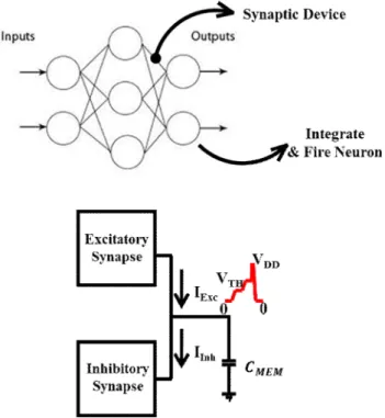
2.1 Neuron Circuit
Biological neurons integrate the signals of the pre-neurons coming through the synapse into the soma. When the integrated signal goes above a certain threshold, it generates an action potential spike through the axon. This integrate & fire characteristic also applies to the neuron circuit in the neuromorphic system which imitates the biological nervous system [1,2]. In the neuron-synapse multilayer, signals coming from the synaptic device are integrated in the capacitor of the neuron circuit. When the signal is generated from the neuron, the generated signal is transferred to the post-synapses. At the same time, signal is fed back to the pre-synapses, and the weight of the pre- synapses can be changed through the characteristics of Spike-Timing-
Dependent-Plasticity (STDP) or Spike-Rate-Dependent-Plasticity (SRDP).
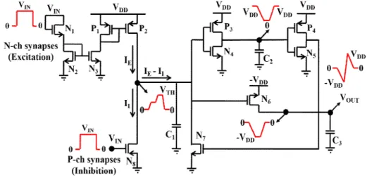
A proposed neuron circuit is shown in Fig. 2.1., which generates asymmetric output spikes that can drive the synaptic device. The proposed neuron circuit has integrate & fire characteristics like biological neurons, and uses only NMOS, PMOS, and capacitors, and has simple structure such as inverter and current mirror. First, the capacitor labeled C1 integrates signal comes from the pre- synapses like the soma of the biological neuron. When the signal integrated in the capacitor goes above a certain level and exceeds the threshold, the NMOS connected with -VDDindicated by N6operates first and pulls the output node
Figure 2.1.Integrate & Fire Neuron circuit having an asymmetric output characteristic.
voltage to -VDD.At the same time, at the two inverter stages connected in series, the output node is pulled back to +VDD when the second inverter operates, ensuring a sufficient delay to be pulled to -VDD. Finally, the output node voltage pulled to +VDD again drives the NMOS labeled N7 to return the output node voltage to its original state by discharging capacitor C1.The fabricated circuit diagram is shown in Fig 2.2.
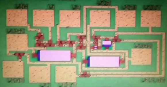
Figure 2.2.Top view of the fabricated neuron circuit.
2.2 Synaptic Device
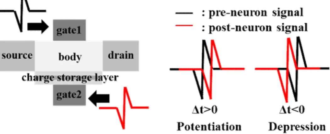
The above-mentioned neuron circuit with asymmetric output spike characteristic circuit is designed to drive the previously proposed 4-terminal silicon based floating body synaptic transistor (SFST) [3,4]. As shown in Fig 2.3., there is an ONO stack with a double gate structure that can store charge at the
‘gate2’ side. If excess carriers are generated by impact-ionization when the device is operating, carriers can be stored in the charge storage layer. Therefore, it is possible to change the weight of the synaptic device according to the degree of a presence of carriers in the ONO stack by the timing difference between pre- neuron and post-neuron signals coming into gate1 and gate2 respectively [5].
Figure 2.3.Structure and learning mechanism of the SFST.
2.3 Weight Transfer Method
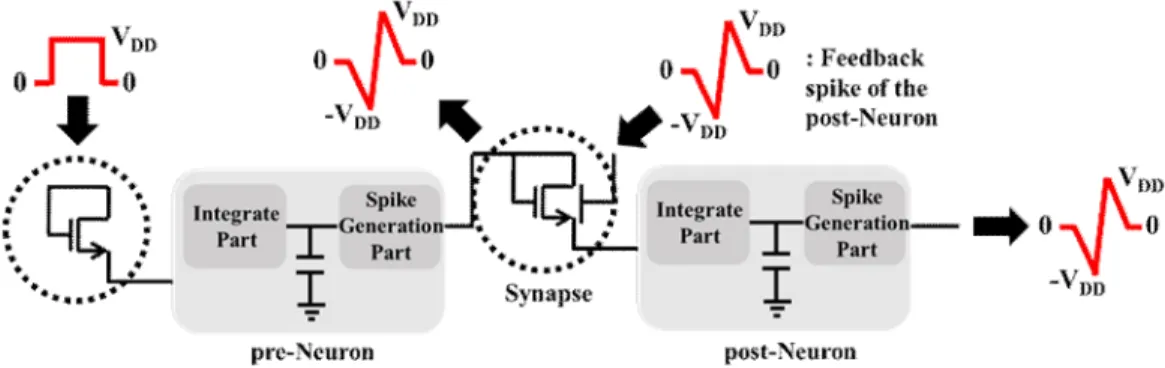
In Fig 2.4, simple neuromorphic system with neuron-synapse connection is shown. Just like biological neural system, signals from pre-neuron is transferred to post-neuron by synaptic device, which can store appropriate weight. Weight of the synaptic device can be modulated with timing difference of pre-synaptic neuron and post-synaptic neuron by mimicking biological STDP characteristics.
When square input pulse is applied to the pre-synapse which is replaced to simple NMOS, pre-neuron integrates the signal and finally generates output spike as mentioned above. In this situation, the output spike of the neuron circuit which is measured value and characteristics of the synaptic device is modeled and verified using SILVACO SMART SPICE simulation tool. In the case of Δt >
0, where Δt is a timing difference of the post-neuron and the pre-neuron spike applied into the synapse, a positive bias is applied to the top gate of the synaptic device and a negative bias is applied to the bottom gate. After this learning process, synaptic device flows more current when the same input is applied again. Similarly, in the case of Δt < 0, a negative bias is applied to the top gate
Figure 2.4.Simple neuromorphic system configuration with connection of the neuron and synapse.
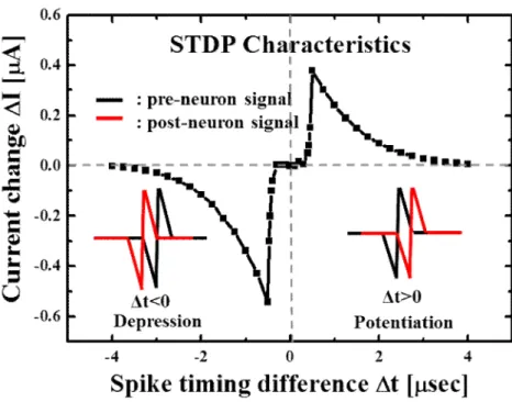
Figure 2.5.STDP characteristics of the neuromorphic system in Fig. 2.4.
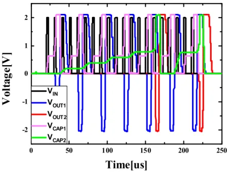
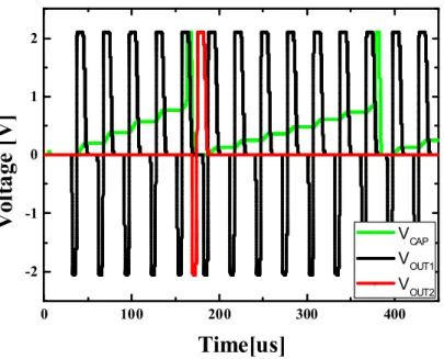
and a negative bias is applied to the bottom gate causing less current to flow when the same input is applied after learning. STDP characteristics of the neuromorphic system constructed in Fig. 2.4 is shown in Fig. 2.5. By applying feedback spike into the bottom gate of the synapse with various timing difference, the weight change of the intermediate synapse is verified with well- known STDP characteristics in biological neural systems [6]. Therefore, we know that the weight of the synapse can be changed according to the STDP characteristics. As shown in Fig 2.6, and Fig 2.7, charging speed of the capacitor varies. In the case of Δt > 0, capacitor charges faster because of the holes in ONO stack of the SFST. On the other hand, in the case of Δt < 0, capacitor charges more slowly due to the electrons in ONO stack. As a result, it can be seen that the weight of the synaptic device can be changed by the timing difference between the pre-synaptic neuron and post-synaptic neuron. This also means that weights can be appropriately assigned in the weight transfer method.
0 50 100 150 200 250 -2
-1 0 1 2
VIN VOUT1 VOUT2 VCAP1 VCAP2 VIN VOUT1 VOUT2 VCAP1 VCAP2 VIN VOUT1 VOUT2 VCAP1 VCAP2 VIN VOUT1 VOUT2 VCAP1 VCAP2
V ol ta ge [V ]
Time[us]
Figure 2.6.Potentiation of the synaptic device.
0 100 200 300 400
-2 -1 0 1 2
VCAP VOUT1 VOUT2
V ol ta ge [ V ]
Time[us]
VCAP VOUT1 VOUT2
Figure 2.7.Depression of the synaptic device.
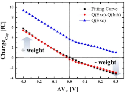
As shown in Fig 2.8, the weight from a well-established non-SNN can be transferred to SNN. If the non-SNN system, learned through the activation function of RELU, Sigmoid, etc., can be applied directly in the hardware based SNN, it has a great advantage in terms of power consumption and efficiency. By using two stage synapse as a synaptic integration part and changing only the weight of excitatory synapse, it is possible to implement +, – weight as in non- SNN. In Fig 2.9, it is shown how + and – weight can be implemented. First, the graph indicated by Q(exc) shows how much charge is accumulated in the membrane capacitor in one pulse by changing VT of excitatory synapse.
Secondly, using inhibitory synapse as a set with excitatory synapse, the charge accumulated on the membrane capacitor can be set to zero when there is no VT
change in excitatory synapse. Finally, if ΔVT is positive, excitatory synapse will flow less current than inhibitory synapse, discharging the membrane cap. In the opposite case, if ΔVT is negative, excitatory synapse will flow larger current than inhibitory synapse, charging the membrane capacitor.
Figure 2.8Schematic view of signal integration part to implement +, - weight.
Figure 2.9Weight transfer from software-based simulation
Weight map of 1-layer MNIST simulation in non-SNN is shown in Fig 2.10. The 1-layer MNIST pattern recognition simulation using MATLAB showed error rate of 7.33%, which means 733 of 10000 test samples were determined as errors. The Rectified Linear Unit(ReLU) is used as an activation function.
Figure 2.10. Weight map of non-SNN based 1-layer MNIST simulation (Error rate:
7.33%).
2.4. System Configuration
Synaptic device, neuron circuit, system configuration for +, – weight and weight transfer method can be used to form an overall neuromorphic system using
SNN. In particular, for the + and – weight implementations, inhibitory synapse
must flow the same amount of current as the excitatory synapse with ΔVT=0 when
the signal is received. In order to construct inhibitory part serving as a constant
current source, we composed pseudo-current source that can constantly discharge
the membrane capacitor which is shown in Fig 2.11. By using synaptic device and
simple current mirror, it can mimic the characteristics of the voltage controlled
current source.
Figure 2.11.Inhibitory synapse connection to flow constant current.
In Fig 2.12, using the MNIST test sample, it is shown that the currents are same with
VCCS and the pseudo-current source using the current mirror. With constant
inhibitory current, VT map of excitatory synapse which is shown in Fig 2.10 can be
exactly given in SNN. Therefore, regardless of the spike generation part, the weight
between layers can be determined in the integration part of the circuit. A comparison
of MNIST pattern recognition test sample ‘0’ using VCCS and the pseudo-current
source in the neuron corresponding to the digit ‘4’ is shown in Fig 2.13.
Figure 2.12. Compared IInhitory-T curves of Voltage Controlled Current Source and inhibitory part using current mirror.
Figure 2.13. Comparison of membrane capacitor voltage of the MNIST test sample ‘0’
using VCCS and pseudo-current source.
Chapter 3
Implementation of Neuromorphic System
3.1 1-Layer MNIST Pattern Recognition
Integrate and fire neuron circuit consists of integration part and spike
generating part is used to implement neuromorphic system as mentioned above. In Fig
3.1, overall system construction is shown. Integration part receives input signal and
integrate the current at membrane capacitor which consists of excitatory part and
inhibitory part. In spike generating part, when the capacitor voltage is above threshold, a
Figure 3.1. Integrate & Fire neuron circuit consists of integration part and spike generating part.
pMOS pulls up the capacitor voltage and series of inverter, nMOS, pMOS generate
asymmetric output pulse. The MNIST is large database of handwritten digits which is
commonly used for training image processing systems. In order to test 28ⅹ28 MNIST
pattern recognition, input stage consists of 784 excitatory synapses. As shown in Fig 3.2,
same number of inhibitory synapses are used to match excitatory synapse each. The pair
of excitatory and inhibitory synapse represent one pixel of 28ⅹ28 MNIST pattern. The
output stage consists of 10 equivalent neuron, each represent digit 0 to 9. By identifying
the most frequently firing neurons among the 10 neurons, we can assert what digit the
input is recognized as.
Figure 3.2.Schematic view of 1-layer MNIST pattern recognition simulation. Input stage consists of 784 synapses and output stage is constructed with 10 neurons.
3.1.1. Right-justified Rate Coding
By using spike rate coding, MNIST pattern recognition is conducted. Right-
justified rate coding, which is also called frequency coding, is a traditional coding
scheme assuming that stimulus is contained in the firing rate of the neuron as shown in
Fig 3.3. Therefore, the stronger the signal intensity within a certain time scale, the
greater the number of fires. Since it is proceeded with 256 gray scale, in the case of
right justified rate coding, the signal comes in at regular intervals, and as the intensity of
the signal increases, the signal starts to come in first. For example, the signal with the
highest intensity produces 255 spikes, while the signal with the lowest intensity does not
produce spikes. To ensure MNIST is implemented correctly at SNN, 14thMNIST test
Figure 3.3.Schematic view of right justified rate coding and overall system configuration using synaptic device, neuron circuit, weight transfer method.
sample is verified. For the time scale, the process was performed from 255 times to
510us with 2us intervals per signal. In Fig 3.4, raster plot of MNIST test sample ‘0’ is
shown. Since right justified rate coding is used, more neurons tend to fire as they go to
510us. In the case of the 14th test sample, digit ‘0’ enters as an input and the system
correctly recognizes ‘0’ as shown in Fig 3.4. MATLAB simulation of the SNN system
shows that the neuron corresponding to ‘0’ is the most likely to be fired compared to
other neurons. Fig 3.5 and Fig 3.6 shows SPICE simulation result of the 14thtest sample
in neurons which represent digit ‘0’, ‘2’, ‘5’, and ‘9’.
Figure 3.4.Raster plot of MNIST test sample ‘0’ using right justified rate coding.
Figure 3.5. Membrane capacitor voltage of neuron 0 and neuron 2 with the MNIST test sample ‘0’. Right justified rate coding is used for input.
Figure 3.6. Membrane capacitor voltage of neuron 5 and neuron 9 with the MNIST test sample ‘0’. Right justified rate coding is used for input.
3.1.2. Left-justified Rate Coding
As with right-justified rate coding, the interval between signals is constant
even with left-justified rate coding and multiple spikes begin to come out from the
beginning as the signal becomes stronger. For example, in the case of the strong
signal, spikes start to generate from 0us, and continue for as long as the intensity of
the signal as shown in Fig 3.7. In Fig 3.8, raster plot of the 14th test sample when
using left-justified rate coding is shown. Unlike Fig 3.4, since left-justified rate
coding is used, it is shown that neurons are less fired as they go to 510us.
Figure 3.7.Schematic view of left justified rate coding.
Figure 3.8.Raster plot of MNIST test sample ‘0’ using left justified rate coding.
Figure 3.9Membrane capacitor voltage of neuron 0 with the MNIST test sample ‘0’. Left justified rate coding is used for input.
Figure 3.10 Membrane capacitor voltage of neuron 2 and neuron 5 with the MNIST test sample ‘0’. Left justified rate coding is used for input.
In Fig 3.9 and Fig 3.10, it is verified that the simulated neuromorphic system can
equivalently reflect the software based non-SNN simulation which used RELU as a
activation function. Compared with Fig 3.8, although the number of firing is not exactly
the same, circuit simulations show that the neurons fire at almost the same rate as the
non-SNN, recognizing handwritten digit ‘0’ correctly. As with right-justified rate coding,
the most frequent firing occurred in the case of neuron 0, and the 14th test sample
corresponding to ‘0’ was confirmed to be well-checked by the system.
SNN-based SPICE simulations and non-SNN based MATLAB simulations show
equivalent results, which means that weights in well-established non-SNNs using back-
propagation can be appropriately transferred to the SNN.
3.2 Overflow Retaining Neuron Circuit
In Fig 3.11, overflow retaining neuron circuit with different structure of spike
generating part from the conventional neuron circuit is shown. By setting virtual
membrane node differently from conventional neuron circuit, spikes can be generated
independently of the membrane capacitor voltage. In the overflow retaining circuit, the
membrane capacitor merely integrates the signal coming from the integration part, and
when the neuron fires, the capacitor discharges only by VT. Also, even though the value
of the membrane capacitor is near VT through the inverter stage, the voltage is pulled up
to VDDat virtual membrane node, so no separate feedback device is needed.
Figure 3.11.Overflow retaining neuron circuit.
For the rest of the operation, it operates in the same way as the circuit shown in Fig 2.1.
Through the two cascaded inverter stages, virtual membrane node can be defined, which
can produce the same output pulse as the previous neuron circuit. At the same time, in
the case of the membrane capacitor node, the integration of the signal and the discharge
of capacitor can proceed independently. The reason why the discharge must occur in the
capacitor only by VTis shown in Fig 3.12. When the neuron fires, if the incoming signal
exceeds VT, the remaining signal is wasted. In the case of conventional neuron circuit, if
VT is exceeded, membrane capacitor node will be unconditionally pulled up to VDD so
there will be a wasted signal every time neuron is fired. However, in the case of
Figure 3.12.Comparison of membrane capacitor voltage of conventional neuron circuit
and overflow retaining neuron circuit.
Figure 3.13. Comparison of simulated membrane capacitor voltage of conventional
neuron circuit and overflow retaining neuron circuit.
overflow retaining neuron circuit, the virtual membrane can replace the membrane of
the conventional neuron circuit, allowing the membrane capacitor node to be discharged
only at VTwhen neuron is fired. In Fig 3.13, comparison of the simulated membrane
capacitor voltage of conventional neuron circuit and overflow retaining neuron circuit is
shown. Since the overflow retaining circuit discharges exactly VT, the overflow can be
stably maintained without the wasted signal. At the same time, it can be confirmed that
asymmetric output pulse is generated as well as conventional neuron circuit.
Figure 3.14. Raster plot of MNIST test sample ‘3’ using right justified rate coding and
conventional integrate and fire neuron circuit.
From Fig 3.14 to Fig 3.17, 529th test sample is used which is handwritten digit ‘3’, but
‘2’ or ‘3’ is determined by a very fine difference. In Fig 3.14, raster plot of the MNIST
test sample ‘3’ is shown. Right-justified rate coding is used with conventional integrate
and fire neuron circuit. However, this test sample concludes that the neuron 2 and
neuron 3 fired the same number of times, which turns out to be an error. On the other
hand, when overflow retaining circuit is used, it can be seen from the Fig 3.15 that the
neuron 3 is fired once more than the neuron 2, so that it is recognized correctly.
Figure 3.15. Raster plot of 529th test sample using right justified rate coding and
overflow retaining neuron circuit
As in the previous 14thtest sample, it is shown in Fig 3.16 and Fig 3.17 whether the
same result as the raster plot is obtained in the actual SPICE simulation. In Fig 3.16, as
in Fig 3.14 which uses conventional integrate and fire neuron circuit, the neuron 2 and
neuron 3 fired the same number of times and recognized as an error. On the other hand
with overflow retaining neuron circuit, it is verified in Fig 3.17 that it recognizes the
digit ‘3’ correctly like raster plot in Fig 3.15 by keeping the overflow.
Figure 3.16. Membrane capacitor voltage of neuron 2 and neuron 3 with MNIST test
sample ‘3’. Right justified rate coding is used for input.
Figure 3.17. Membrane capacitor voltage of neuron 2 and neuron 3 with MNIST test
sample ‘3’. Right justified rate coding is used for input.
Chapter 4 Conclusions
In this thesis, neuromorphic system has been introduced which can perform MNIST pattern recognition. In addition, the overflow retaining neuron circuit which can improve the accuracy more easily through simple structure change have been demonstrated. This system implemented by SPICE simulation can be used not only for MNIST pattern recognition but also for all kinds of artificial neural network related systems such as voice recognition, face recognition at hardware level instead of software. The STDP characteristics that can modulate synaptic weight, are analyzed in SPICE simulation by connecting previously proposed synaptic device and neuron circuit. The weight can be determined by VTof the synaptic device and it is confirmed that + and – weight in the software can be equivalently implemented in SNN system, through inhibitory part of the neuron circuit. Also, 1-layer artificial neural network is specifically investigated by implementing 1-layer SNN neuromorphic system using SILVACO SMARTSPICE simulation tool. In the simulation result, the result of MATLAB
simulation and SPICE simulation are almost the same. In order to increase the accuracy, the operation of the overflow retaining neuron circuit to minimize the wasted signal is confirmed. Case study shows that overflow retaining neuron circuit improves the accuracy MNIST pattern recognition.
Bibliography
[1] Bishop, Christopher M. "Pattern recognition." Machine Learning 128 (2006) pp. 1-58
[2] Muda, Lindasalwa, Mumtaj Begam, and Irraivan Elamvazuthi. "Voice recognition algorithms using mel frequency cepstral coefficient (MFCC) and dynamic time warping (DTW) techniques." arXiv preprint arXiv:1003.4083 (2010).
[3] Bench-Capon, Trevor JM, and Paul E. Dunne. "Argumentation in artificial intelligence." Artificial intelligence 171.10-15 (2007): 619-641.
[4] BERRAL, Josep Ll, et al. Towards energy-aware scheduling in data centers using machine learning. In: Proceedings of the 1st International Conference on energy-Efficient Computing and Networking. ACM, 2010.
p. 215-224.
[5] Fan, D., Shim, Y., Raghunathan, A., & Roy, K. (2015). STT-SNN: A spin- transfer-torque based soft-limiting non-linear neuron for low-power artificial neural networks. IEEE Transactions on Nanotechnology, 14(6), 1013-1023.
[6] Basheer, I. A., and M. Hajmeer. "Artificial neural networks: fundamentals, computing, design, and application." Journal of microbiological methods 43.1 (2000): 3-31
[7] Li, Boxun, et al. "Training itself: Mixed-signal training acceleration for memristor-based neural network." Design Automation Conference (ASP- DAC), 2014 19th Asia and South Pacific. IEEE, 2014.
[8] Kasabov, Nikola K. "NeuCube: A spiking neural network architecture for mapping, learning and understanding of spatio-temporal brain data." Neural Networks 52 (2014): 62-76.
[9] Burr, Geoffrey W., et al. "Experimental demonstration and tolerancing of a large-scale neural network (165 000 synapses) using phase-change memory as the synaptic weight element." IEEE Transactions on Electron Devices 62.11 (2015): 3498-3507.
[10] Dytckov, Sergei, et al. "Efficient STDP Micro-Architecture for Silicon Spiking Neural Networks." Digital System Design (DSD), 2014 17th Euromicro Conference on. IEEE, 2014.
[11] Chen, Dan, et al. "Brain big data processing with massively parallel computing technology: challenges and opportunities." Software: Practice and Experience 47.3 (2017): 405-420
[12] Deng, Lei, et al. "Ultra low power of artificial cognitive memory for brain-like computation." Nanoelectronics Conference (INEC), 2014 IEEE International. IEEE, 2014.
[13] Monroe, Don. "Neuromorphic computing gets ready for the (really) big time." Communications of the ACM 57.6 (2014): 13-15.
[14] Chou, Teyuh, et al. "Neuromorphic pattern learning using HBM electronic synapse with excitatory and inhibitory plasticity." VLSI Technology, Systems and Application (VLSI-TSA), 2015 International Symposium on.
IEEE, 2015.
[15] Diehl, Peter U., et al. "Conversion of artificial recurrent neural networks to spiking neural networks for low-power neuromorphic hardware."
Rebooting Computing (ICRC), IEEE International Conference on. IEEE, 2016.
[16] Mahalanabis, D., et al. "Incremental resistance programming of programmable metallization cells for use as electronic synapses." Solid- State Electronics 100 (2014): 39-44.
[17] Eryilmaz, S. Burc, et al. "Device and system level design considerations for analog-non-volatile-memory based neuromorphic architectures."
Electron Devices Meeting (IEDM), 2015 IEEE International. IEEE, 2015.
[18] Wan, Xiang, et al. "Simulation of Laterally Coupled InGaZnO 4-Based Electric-Double-Layer Transistors for Synaptic Electronics." IEEE Electron Device Letters 36.2 (2015): 204-206.
[19] Kim, Sungjun, et al. "Gradual bipolar resistive switching in Ni/Si 3 N 4/n+-Si resistive-switching memory device for high-density integration and low-power applications." Solid-State Electronics 114 (2015): 94-97.
[20] Prezioso, Mirko, et al. "Training and operation of an integrated neuromorphic network based on metal-oxide memristors." Nature 521.7550 (2015): 61-64.
[21] Merolla, Paul A., et al. "A million spiking-neuron integrated circuit with a scalable communication network and interface." Science 345.6197 (2014):
668-673.
[22] Chu, Myonglae, et al. "Neuromorphic hardware system for visual pattern recognition with memristor array and CMOS neuron." IEEE Transactions on Industrial Electronics 62.4 (2015): 2410-2419.
[23] Kim, Hyungjin, et al. "Simulation Study on Silicon-Based Floating Body Synaptic Transistor with Short-and Long-Term Memory Functions and Its Spike Timing-Dependent Plasticity." JOURNAL OF SEMICONDUCTOR TECHNOLOGY AND SCIENCE 16.5 (2016): 657-663.
[24] Kim, Hyungjin, et al. "Silicon-Based Floating-Body Synaptic Transistor With Frequency-Dependent Short-and Long-Term Memories." IEEE Electron Device Letters 37.3 (2016): 249-252.
[25] Park, Jungjin, et al. "Neuromorphic System Based on CMOS Inverters and Si-Based Synaptic Device." Journal of Nanoscience and Nanotechnology 16.5 (2016): 4709-4712.
[26] Subramaniam, Anand, et al. "Spike-timing-dependent plasticity using biologically realistic action potentials and low-temperature materials."
IEEE Transactions on Nanotechnology 12.3 (2013): 450-459.
초 록
인 간 을 대 신 할 수 있 는 음 성 인 식, 얼 굴 인 식, 자 율 작 업 과 같 은 인 공 지 능 기 술 은 큰 화 제 를 불 러 일 으 켜 왔 고, 세 계 적 인 추 세 에 서 미 래 의 산 업 시 장 을 바 꿀 것 이 다. 하 지 만 폰 노 이 만 구 조 에 기 인 한 현 재 의 컴 퓨 팅 시 스 템 의 경 우 에 는 파 워 소 모 와 효 율 성 측 면 에 서 문 제 점 을 보 여 왔 다. 특 히 고 차 원 적 인 연 산 을 수 행 할 때 많 은 양 의 정 보 를 처 리 하 면 서 비 효 율 성 과 큰 전 력 소 모 로 일 어 나 게 되 는 폰 노 이 만 병 목 현 상 은 새 로 운 인 공 지 능 시 스 템 을 야 기 하 였 다. 뉴 로 모 픽 시 스 템 의 효 용 성 을 확 인 하 기 위 해 시 냅 스 소 자 와 뉴 런 회 로 로 구 성 된 스 파 이 킹-뉴 럴-네 트 워 크 에 대 해 면 밀 하 게 연 구 하 였 다. 전 자 회 로 시 뮬 레 이 션 을 통 해 손 글 씨 패 턴 인 식 을 진 행 하 였 을 때, 뉴 로 모 픽 시 스 템 이 MATLAB을 통 해 구 현 한 인 공 신 경 망 과 같 은 결 과 를 보 임 을 확 인 하 였 다. 이 것 은 소 프 트 웨 어 기 반 으 로 구 현 된 모 든 인 공 지 능 시 스 템 을 하 드 웨 어 적 으 로 그 대 로 옮 겨 와 서 구 현 할 수 있 음 을 의 미 한 다. 또 한, 손 글 씨 패 턴 인 식 의 정 확 도 를 개 선 하 기 위 해, overflow retaining 뉴 런 회 로 를 제 안 하 였 다. 간 단 한 회 로 구 조 의 변 화 를 통 해 가 상 의 노 드 가 적 절 하 게 동 작 하 였 으 며, 기 존 의 int egrate and fire 뉴 런 회 로 와 다 르 게 낭 비 되 는 신 호 를 최 소 화 하 였 다. 이 러 한 사 실 은 MATLAB 시 뮬 레 이 션 에 서 추 출 한
raster plot과 전 자 회 로 시 뮬 레 이 션 의 결 과 를 비 교 함 으 로 써 확 인 되 었 고 다 른 인 공 신 경 망 구 조 가 하 드 웨 어 적 으 로 구 현 될 수 있 음 을 의 미 한 다.
주요어 : 뉴로모픽 시스템, 스파이킹 뉴럴 네트워크, 뉴런, 시냅스, 과 도신호 유지.
학번 : 2016-20956`