저작자표시-비영리-변경금지 2.0 대한민국 이용자는 아래의 조건을 따르는 경우에 한하여 자유롭게
l 이 저작물을 복제, 배포, 전송, 전시, 공연 및 방송할 수 있습니다. 다음과 같은 조건을 따라야 합니다:
l 귀하는, 이 저작물의 재이용이나 배포의 경우, 이 저작물에 적용된 이용허락조건 을 명확하게 나타내어야 합니다.
l 저작권자로부터 별도의 허가를 받으면 이러한 조건들은 적용되지 않습니다.
저작권법에 따른 이용자의 권리는 위의 내용에 의하여 영향을 받지 않습니다. 이것은 이용허락규약(Legal Code)을 이해하기 쉽게 요약한 것입니다.
Disclaimer
저작자표시. 귀하는 원저작자를 표시하여야 합니다.
비영리. 귀하는 이 저작물을 영리 목적으로 이용할 수 없습니다.
변경금지. 귀하는 이 저작물을 개작, 변형 또는 가공할 수 없습니다.
공 학 석 사 학 위 논 문
실시간관찰 기술을 위한 통전 인장
투과전자현미경 홀더의 설계 및 적용에 관한 연구
Design and application of electrical-straining TEM holder for in-situ TEM techniques
2018 년 2 월
서울대학교 대학원 재료공학부
홍 석 용
초 록
Electrically Assisted Forming(EAF)는 금속의 성형성을 증가시키기 위한 기술로써, 변형 도중 금속의 성형성을 증가시키거나 성형 후 치수불량을 발생시키는 spring back 현상을 완화시킬 수 있다고 알려져 있다[5]. 일반적으로, 산업계에서는 금속의 성형성을 증가시키기 위한 방안으로 열간성형(hot-forming)을 채택해왔다. 하지만 열간성형은 성형 후 국부적인 온도편차로 인한 잔류응력발생 및 불균일한 미세조직 등의 문제를 안고 있는 상황이다. 때문에 이를 대체할 수 있는 방법들이 개발 및 적용되고 있는 상황이다. 그 중 하나로 금속 판재에 전류를 흘려줌으로써 성형성을 증가시키는 방법이 고안되었다[1]. 최근, EAF process중 재료에 일어나는 변화를 파악하기 위해 학계에서 많은 연구들이 진행되고 있는데, 이는 전기가 재료에 미치 는 영향이 명확하게 정의되지 않았기 때문이다. 본 연구에서는 통전 중 미세조직에 일어나는 변화를 조사하기 위하여 실시간으로 시편에 변형력과 전기력을 동시에 가 해줄 수 있는 투과전자현미경(Transmission Electron Microscope, TEM)용 holder 를 개발하였고, 실제 field test와 output 측정를 통하여 그 성능을 확인한 것에 대 한 내용이다. 개발된 TEM holder는 straining, electrical part로 구성되어 있으며, 본문에서 기술될 내용은 각 part별 구성과 field test, output 측정에 관한 것이다.
Straining part는 크게 mini motor, linear stage, feedthrough의 movement o-ring, zirconia ceramics stage로 구성되어 있다. Field test에서는 인장 중 미세조직에 나 타나는 거동을 관찰하기 위하여 pure aluminum 시편 인장실험이 시행되었고, 이를 통하여 실시간으로 microcrack이 propagation되는 과정을 관찰하였다. 해당 test로
부터 crack tip과 grain boundary로부터 방출되는 dislocation들의 거동을 실시간으 로 관찰할 수 있었고, 이를 통하여 straining part의 동작을 확인하였다. electrical part에 대한 동작 확인을 위하여 K-type thermocouple와 DAQ system을 통한 온 도측정을 수행하였고, arduino board와 relay를 이용하여 구현한 electrical pulse의 파형을 oscilloscope를 통해 측정하였다. Field test에서는 시편에 electrical pulse를 가해줄 때 나타나는 거동을 관찰하기 위하여 pure aluminum 시편의 균열 첨단부에 서의 통전 중 거동을 관찰하였다. 해당 test를 통하여 당초 목표하였던 dislocation 들의 움직임 및 grain boundary의 변화는 관찰하지 못하였지만, 온도 및 파형 등의 pulse output 측정을 통해 electrical part의 성능을 검증하였다. 향후 실제 실험에 적용되어 다양한 금속재료에서 통전 시 발생하는 변화를 관찰하게 된다면 전기가 재료의 미세조직에 미치는 정확한 영향을 파악하는데 크게 기여할 수 있을 것이라 생각된다.
주요어 : EAF, In-situ TEM, straining, electrical pulse, microstructure 학 번 : 2016-20856
이 름 : 홍 석 용
목 차
초 록 ... i
목 차 ... iii
그림 목차 ... v
표 목차 ... viii
제 1장 서론 ... 1
1.1 실시간 관찰기술 ... 1
1.2 EAF(Electrically Assisted Forming) 기술 ... 3
제 2장 Electrical-Straining TEM holder ... 7
2.1 개요 ... 7
2.2 시편제작 ... 9
제 3장 Straining part ... 12
3.1 구성 ... 12
3.2 field test ... 15
3.3 개선점 ... 20
제 4장 Electrical part ... 24
4.1 구성 및 개선점 ... 24
4.2 field test ... 31
제 5장 요약 ... 37
참고 문헌 ... 39
Abstract ... 42
그림 목차
Figure 1. (a) In-situ tensile TEM holder, (b) In-situ electrical probing TEM holder, (c) In-situ liquid cell TEM holder (d) TEM CathodoLuminescence holder
Figure 2. EAF formability improvement (Ti-G5) (a) Conventional forming of a Ti alloy, (b) EAF forming of the same material
Figure 3. Overview of electrical-straining TEM holder and Holder tip
Figure 4. Counterbore type connection of Titanium screw, zirconia ceramics stage, copper electrode
Figure 5. (a) CAD drawing, specimen cutout, (b) Mechanical polishing using sand paper up to 100micrometer thickness, (c) Electrolytic polishing using tenupol-5 jet polisher, (d) Dog-bone specimen and Observation area
Figure 6. Schematic CAD drawing and photograph of straining part
Figure 7. Actual moving distance of specimen area due to motor rotation and observation area
Figure 8. Snapshots of in-situ tensile test of pure aluminum specimen (a) Before tensile (b) Emission of dislocations (c) Crack propagation terminal
Figure 9. Emission of dislocations from grain boundary
Figure 10. Snapshots of in-situ tensile test of pure aluminum specimen (a)Before tensile, (b) Emission of dislocations from crack tip, (c) Dislocation pile up, glide, (d) Crack propagation path thinning, (e) Locally necking, (f) Sharp crack abruptly propagation
Figure 11. (a), (b) Dislocation pile up, (c) Observation area
Figure 12. Replace lead screw with ball screw
Figure 13. Electrical part CAD drawing
Figure 14. Maximize voltage drop in specimen
Figure 15. Schematic of electrical pulse part
Figure 16. Photograph of electrical part
Figure 17. Oscilloscope wave form and plotting
Figure 18. Specimen temperature measurement method
Figure 19. K, R-type thermocouple details
Figure 20. Cross section of specimen and current density
Figure 21. (a) Before reaction, (b) After reaction, (c) Temperature profile
Figure 22. CAD drawing of TEM holder tip and specimen
Figure 23. (a) Before reaction, (b) After reaction (c) Temperature profile
표 목차
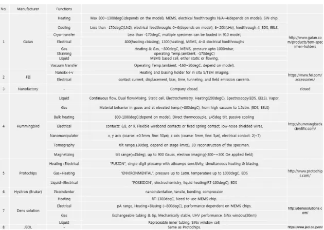
Table 1. In-situ TEM holder manufacturers and commercial products
Table 2. Actuator moving speed corresponding to applied voltage to mini motor
Table 3. Various measured value corresponding to set value and error factor
제 1장 서론
1.1 실시간 관찰기술
In-situ 기술은 외부자극에 의한 재료의 reaction을 실시간으로 관찰할 수 있다는
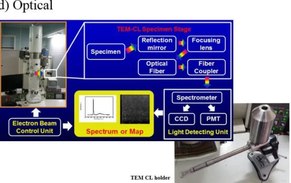
이점을 가진 기술이다. reaction 전, 후의 path를 실시간으로 관찰함으로써 그 정보 를 토대로 실험 시에 적절한 process를 선택할 수 있다. 이러한 장점을 가지기 때문 에 in-situ 기술은 다양한 분야에서 광범위하게 적용될 수 있다. Figure 1은 실시간 관찰전자현미경 연구실에서 개발한 TEM holder들의 사진과 그 내용에 관한 것이 다. 모두 다양한 분야에서 각각의 목적에 부합하도록 설계되어있다. 이처럼 실험의 목적에 부합하는 TEM holder를 설계하고 이를 통해 reaction path를 관찰함으로써 수많은 유용한 정보를 얻을 수 있게 된다.
Figure 1. (a) In-situ tensile TEM holder, (b) In-situ electrical probing TEM holder, (c) In-situ liquid cell TEM holder (d) TEM CathodoLuminescence holder
1.2 EAF(Electrically Assisted Forming) 기술
최근 자동차 및 항공기 업계에서는 연료의 효율성을 위하여 경량금속의 사용이 늘 어나고 있는 상황이다. 이 때문에 가벼우면서도 높은 강도를 가지는 고강도강판 및 aluminum 합금 등의 사용이 증가하고 있는 추세이다. 이러한 특수한 목적을 가지 는 합금들은 일반적으로 상온에서 철강 재료에 비해 난성형성(poor formability)을 가지는 경우가 대부분이기 때문에 이러한 단점을 해결하기 위한 여러 방안들이 대 두되고 있는 상황이다. 금속의 formability를 증가시키기 위한 방안으로 산업계에서 는 주로 금속의 온도를 증가시킴으로써 formability를 증가시키는 열간성형(hot stamping)을 채택하고 있는 상황이다. 하지만 열간성형은 고가의 장비들로 인한 비
용증가, 가열로 인한 금속표면의 고온산화 및 scale생성, 재료와 금형의 점착 및 강 도 감소, 온도 구배로 인한 잔류응력 발생 및 불균일한 미세조직 등 여러 가지 문 제들을 안고 있는 상황이다. 때문에 이를 대체하기 위한 방안들이 모색되는 중인데, 그 중하나로 금속판재에 통전을 해주는 경우 재료의 특성이 변한다는 사실이 밝혀 지고 있다. 특히, 금속의 응력이 변한다는 사실이 다양한 연구들에 의해서 밝혀지고 있고 이를 전기소성(electroplasticity)이라고 칭하게 된다[1]. 이러한 현상을 바탕으 로 전기 소성 현상을 이용하여 성형성을 향상 시킬 수 있다는 Electrically Assisted Forming(EAF) 기술이 등장하였다. 초기에 학계에 보고된 연구결과에 따르면 금속 판재에 연속된 전류를 통전시킴으로써 금속의 flow stress를 큰 폭으로 감소시킬 수 있음이 밝혀졌다[1]. 또한 금속의 변형 간 통전이 인장시험의 경우에는 최대 elongation이 저하되는 반면에 압축시험의 경우에는 큰 폭으로 elongation이 상승함 을 발견하였다[2,3]. 해당연구에서 인장시험 시 최대 elongation이 저하되는 이유는 시편의 단면적이 인장에 따라 좁아졌고 이에 따라서 전기 에너지 밀도(electric energy density)가 커져서 결국 시편이 과한 온도상승에 의해 조기에 파단에 이르 렀다는 것이다. 이러한 결과로 인하여 연속된 통전을 통한 금속판재의 가공 기술은 최대 elongation 저하현상 으로 인하여 사용할 수 없는 상황에 봉착하게 된다. 이후 이러한 문제점을 해결하기 위해 많은 연구들이 시도되었고, 이에 의해서 연속적이 아닌 주기를 가지는 pulse형태의 전류를 흘려주었을 때, 최대 elongation을 일반적 인 인장시의 파단 elongation에 비하여 큰 폭으로 상승시킬 수 있다는 연구결과들이 등장하였다[4]. 이처럼 전류가 금속의 stress에 영향을 미치는 특성을 가지기 때문에 EAF process를 통해 금속판재에 pulse 형태의 전류를 가해주게 되면, 최대
elongation이 증가하고 이에 따라 변형 중 formability가 대폭 증가되거나 변형 후 치수불량을 발생시키는 spring back 현상이 대폭 완화된다고 알려져 있다[5].
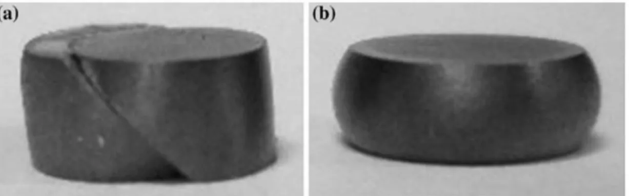
Figure 2는 Titanium 합금에 대한 통전성형 예시를 보여주고 있다. 왼쪽 사진은 통 전을 가하지 않고 압축을 가한 것이며 오른쪽은 통전을 하며 압축한 것이다. 오른 쪽 사진에서 볼 수 있듯이 통전 후에 Titanium 합금의 formability가 큰 폭으로 증 가한 현상을 볼 수 있다.
Figure 2. EAF formability improvement (Ti-G5) (a) Conventinal forming of a Ti alloy, (b) EAF forming of the same material
현재 학계에서는 통전성형 시 전류가 재료에 미치는 정확한 영향을 파악하기 위하 여 여러 가지 연구들이 진행되고 있는 상황인데, 이는 전류가 어떠한 mechanism을 통하여 재료의 물성에 변화를 주는지에 대한 사항이 아직 불분명하기 때문이다. 현 재 학계에 제시되고 있는 가능성을 바탕으로 통전성형 중 전류가 재료에 미치는 영 향은 thermal effect인 joule heating[6]과 athermal effect인 electron wind(electromigration)[7], electrostatic field[8]등이 존재하고 있을 것이라 생각할
수 있다. 하지만 여전히 전류가 재료에 미치는 영향은 불분명하며, 발생하는 변화가 단순 열적인 효과에 의한 것인지 전류만이 가지는 특수한 기능으로 인한 것인지에 대한 확인이 필요한 상황이다. 이러한 열적인 효과와 전류의 효과를 분리하기 위한 방법으로 재료를 목표한 온도까지 단순 가열한 결과와 통전을 통해 목표온도까지 도달시킨 결과를 비교하여 그 차이만큼을 전류에 의한 효과라고 파악하는 간접적인 방법 외에 직접적으로 전류의 효과를 규명한 사실은 그 양이 매우 부족한 실정이 다. 본 연구에서는 통전성형 중 전류가 재료의 미세조직에 미치는 영향을 연구하기 위하여 실시간으로 인장 및 통전이 가능한 TEM holder를 개발하였고 실제 field test와 output measurement를 통하여 그 성능을 검증하고자 하였다. 이를 통하여 통전 중 미세조직에 나타나는 변화를 관찰하게 되면 전류가 재료에 미치는 영향을 파악하는데 큰 기여를 할 수 있을 것이라 생각된다.
제 2장 Electrical-Straining TEM holder
2.1 개요
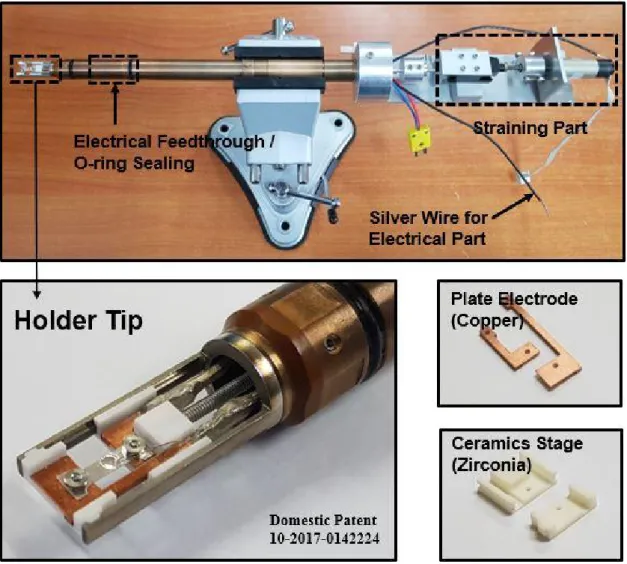
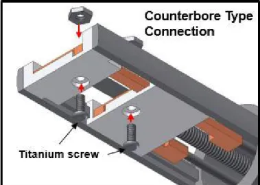
Figure 3은 개발된 Electrical-Straining TEM holder의 전체적인 모습이다. 개발된 홀더는 크게 electrical part와 straining part로 구성되어 있으며, 각 파트에 대한 자 세한 내용은 아래에서 서술하도록 한다. 먼저 TEM holder의 tip부분을 보면 구리로 구성된 판상의 전극, zirconia로 만들어진 ceramics stage, dog-bone 형태의 시편을 볼 수 있다. 이들은 Figure 4에서 볼 수 있듯이 titanium screw가 하단에서 들어가 상단에서 nut로 고정되는 counter bore type으로 체결된다. Holder tip에 위치한 stage의 두께는 3mm이며 실시간관찰전자현미경 연구실에서 보유한 JEOL 2010F TEM goniometer에 적합하도록 설계되었다. 개발된 holder는 시편에 실시간으로 pulse 형태의 고 전류와 인장력을 동시에 가할 수 있다는 점에서 그 장점을 가진다.
Figure 3. Overview of electrical-straining TEM holder and Holder tip
Figure 4. Counterbore type connection of Titanium screw, zirconia ceramics stage, copper electrode
Table 1은 현재 commercial in-situ TEM holder를 제작하는 회사들에 대한 정보를 정리한 표이다. 현재 commercial 제품들 중에서는 자체적으로 시편에 high pulse current 와 인장력을 가할 수 있는 제품은 존재하지 않는다. 또한 시편에 전기력을 가해줄 수 있는 holder들의 기능도 모두 high voltage, low current에 특화된 제품 들이다.
Table 1. In-situ TEM holder manufacturers and commercial products
2.2 시편제작
Figure 5는 제작된 TEM holder에 사용되는 시편에 대한 그림과 그 제작과정이다.
CAD를 이용한 도면작성 및 가공, struers twin polisher와 sand paper를 이용한 100μm 두께까지의 기계적 연마, struers tenupol-5 jet polisher를 이용한 전해 연마
를 거쳐 시편을 완성하였다. jet polishing은 TEM 관찰 시 beam center가 위치하게 될 시편끝단으로부터 4.6mm 떨어진 지점에 진행되었다. 실험 진행시 사전인장을 통하여 pre-crack을 발생시키고 해당영역에 대해 관찰을 진행하였다.
Figure 5. (a) CAD drawing, specimen cutout, (b) Mechanical polishing using sand paper up to 100micrometer thickness, (c) Electrolytic polishing using tenupol-5 jet polisher, (d) Dog-bone specimen and Observation area
제 3장 straining part
3.1 구성
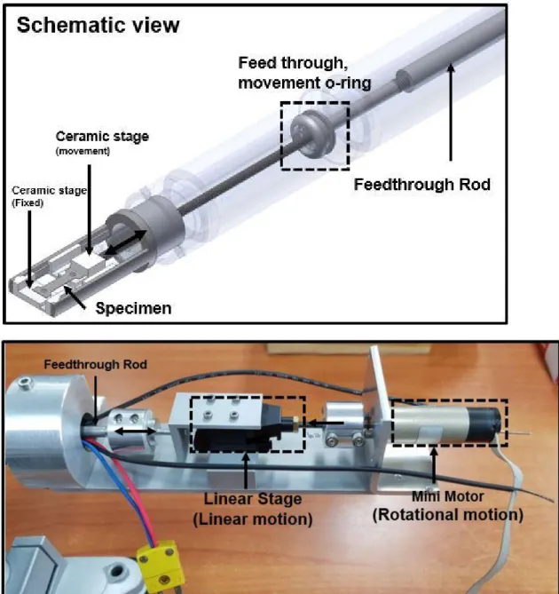
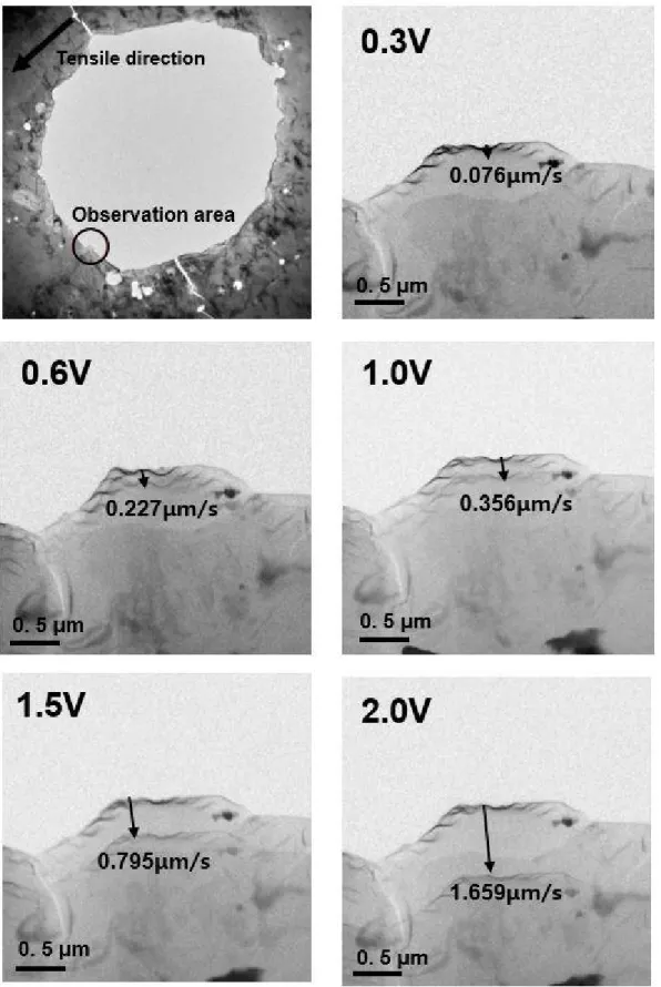
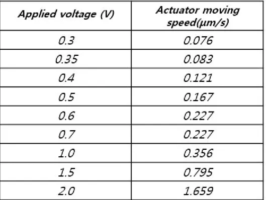
Straining part는 크게 mini motor, linear stage, feedthrough의 movement o-ring, ceramics stage로 구성되어 있다(Figure 6). movement mechanism은 mini motor에 서 시작된 rotational motion이 linear stage, feedthrough rod등의 thread들을 통하 여 linear motion으로 변환된다. 변환된 linear motion은 feedthrough의 movement o-ring을 통하여 ceramics stage로 전달되고 결과적으로 ceramics stage가 움직이 게 된다. 시편의 한쪽 hole은 screw를 통하여 ceramics stage위에 고정되어 있기 때문에, 최종적으로 해당 mechanism을 통하여 시편에 변형이 가해지게 된다. 이때 stage의 movement range는 8.65mm로 큰 수치를 가지고 있다. Figure 7은 시편 인 장 시 mini motor에 인가한 전압에 따른 시편의 실제 초당 displacement를 측정한 그림이다. 관찰영역에서 시편이 실제이동 하는 영상을 촬영 후 이를 frame별 image 로 변환시키고 이것을 바탕으로 displacement를 측정하였다.
Figure 6. Schematic CAD drawing and photograph of straining part
Figure 7. Actual moving distance of specimen area due to motor rotation and observation area
Table 2에서 볼 수 있듯이 mini motor의 최소 동작전압은 0.3V이며 이 때 actuator speed는 0.076μm/s이다.
Table 2. Actuator moving speed corresponding to applied voltage to mini motor
3.2 field test
Figure 8은 straining part의 field test를 위해 pure aluminum 시편을 인장하고 이 에 따른 microcrack propagation을 실시간으로 관찰한 영상에 대한 snapshot들이다.
Figure 8. Snapshots of in-situ tensile test of pure aluminum specimen (a) Before tensile (b) Emission of dislocations (c) Crack propagation terminal
해당 test에서는 crack tip, grain boundary로부터 방출되는 dislocations 및 microcrack propagation을 관찰할 수 있다. 이때 mini motor에 가해지는 전압은 0.3V이며, actuator speed는 0.076μm/s이다. Figure 9는 crack tip상단에 위치한 grain을 확대한 영상에 대한 snapshot들이다. 해당 영상에서는 초기 grain boundary 로부터 방출되어 아래로 이동하는 dislocation들을 관찰할 수 있으며, 잠시 후 또 다 른 slip system이 작동하여 오른쪽으로 이동하는 partial dislocation들을 관찰 할 수 있다.
Figure 9. Emission of dislocations from grain boundary
Figure 10는 또 다른 tensile field test에 관한 영상의 snapshot들이다. 초기 crack 에 인장력이 가해지게 되면 crack이 양쪽으로 확장되며 crack tip 방향으로 dislocation들이 방출된다. 방출된 dislocation들은 crack tip 앞쪽에서 pile up되고 이 후 crack이 propagation됨에 따라 glide하게 된다. 잠시 후 crack propagation path
가 thinning되며 locally necking이 발생하고 급격한 sharp crack propagation이 이 루어진다. 해당 field test들을 통하여 개발된 electrical-straining TEM holder의 straining part에 대한 성능을 확인하였다.
Figure 10. Snapshots of in-situ tensile test of pure aluminum specimen (a)Before tensile, (b) Emission of dislocations from crack tip, (c) Dislocation pile up, glide, (d) Crack propagation path thinning, (e) Locally necking, (f) Sharp crack abruptly propagation
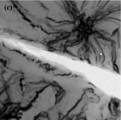
3.3 개선점
Figure 11은 개발된 TEM holder의 design flaw에 대한 영상의 snapshot들이다. 영 상에서는 crack 앞쪽에 위치한 region에서 dislocation들이 조금씩 pile up되는 현상 을 관찰할 수 있다. 해당 영상은 인장 후 mini motor의 동작이 멈춘 상태인데, 이는 인장 후 holder의 joint 부위가 제자리로 돌아오며 발생한 잔류응력의 영향으로 마 치 strain이 존재 하는듯한 현상을 볼 수 있다. 이는 향후 design 수정 작업에서 joint의 수를 줄임으로써 개선할 수 있다.
Figure 11. (a), (b) Dislocation pile up, (c) Observation area
Figure 12은 제작된 holder의 further improvement에 관한 내용이다. ball screw는 screw와 nut사이에 ball을 위치시킴으로써 마찰마모를 큰 폭으로 줄이는 효율적인 방식이다. 현재 feedthrough와 ceramics stage를 연결하는 rod는 lead screw방식으 로 체결되어있는데, 이를 ball screw type으로 교체하게 되면 holder의 동작을 더욱 안정적으로 구현할 수 있을 것이다.
Figure 12. Replace lead screw with ball screw
제 4장 electrical part
4.1 구성 및 개선점
Figure 13는 electrical-straining TEM holder의 electrical part에 대한 CAD drawing이다. electrical part는 크게 copper plate electrode, silver wire, electrical feedthrough로 이루어져있다. electrode에 연결되어 있으며 feedthrough를 통해 외부 로 빠져나간 silver wire는 별도로 설치된 electrical pulse인가 part에 연결되어 결과 적으로 시편에 전기력을 가해주게 된다.
Figure 13. Electrical part CAD drawing
Figure 14에서 볼 수 있듯이 시편 부위에서의 voltage drop를 최대화해주기 위하여
나머지 도선부분의 저항을 최소화 해주었다.
Figure 14. Maximize voltage drop in specimen
Figure 15는 TEM holder를 제외한 별도의 part에 대한 모식도이다. electrical pulse 를 구현하기 위하여 arduino board와 relay를 이용하였으며, arduino board는 relay 에 high/low signal을 보내는 역할을 하며 relay는 이를 input에서 받아들여 output 쪽 회로를 open/close 시켜주는 switch 역할을 한다. relay의 output쪽에 위치한 회 로에는 항상 전원을 공급하고 있는 power supply와 TEM holder가 위치하게 되는 데, relay가 회로자체를 open/close해줌으로써 결과적으로 시편에 전기력을 pulse형 태로 가해줄 수 있게 된다. Figure 16는 electrical part를 구성하는 power supply, arduino board, relay, TEM holder에 대한 실제사진이다.
Figure 15. Schematic of electrical pulse part
Figure 16. photograph of electrical part
table 3은 다양한 set value에 대한 measured value에 대한 값을 나타낸 표이다. 여
기서 set value는 arduino를 통해 설정한 pulse의 on-time 그리고 measured value 는 이를 oscilloscope를 통해 실제로 측정한 수치이다. relay가 동작하는 최소 set value는 8ms이며, 이때의 measured value는 1.5ms이다. set value가 낮은 구간에서 는 measured value대비 오차율이 굉장히 큰 것으로 나타나고 있으며, set value 약 50ms 이상부터 measured value와 1:1로 matching되는 것으로 나타났다. set value 50ms이하 영역에서는 calibration을 진행하여야 한다.
Figure 17. Oscilloscope wave form and plotting
Table 3. Various measured value corresponding to set value and error factor
Figure 18은 시편에 부착된 K-type thermocouple을 보여주고 있다. thermocouple은 ceramics adhesive를 통하여 시편에 부착되어있다. 부착에 ceramic adhesive가 사용
된 이유는 시편과 thermocouple이 전기적으로 절연되어야하기 때문인데, 이는 thermocouple이 금속 쌍에 가해지는 열에 따라 발생하는 일정한 기전력을 토대로 온도를 환산하는 방식이기 때문에 실험 중 시편에 가해지는 electrical pulse가 온도 측정을 방해하기 때문이다. K-type thermocouple은 electrical feedthrough를 통해
외부에 위치한 DAQ system과 연결되어 온도를 측정하게 된다.
Figure 18. Specimen temperature measurement method
Figure 19은 K, R-type thermocouple에 대한 상세사항이다. 현재 사용되고 있는 K-type thermocouple을 R-type으로 교체할 계획에 있다. K-type은 음극에 포함되 는 Nickel과 Aluminum으로 인하여 자성을 띄게 되는데, 이는 TEM의 electron beam을 휘게 만드는 영향을 줄 수 있기 때문에, 자성의 띄지 않으면서 더 높은 온 도영역에서 까지 사용할 수 있는 R-type thermocouple을 사용하게 되면 더욱 안정 적인 holder 동작을 구현할 수 있다.
Figure 19. K, R-type thermocouple details
4.2 field test
Figure 20은 시편 관찰영역의 단면도이며, jet polishing의 영향을 반영하여 modeling하였고 이를 바탕으로 current density를 계산하였다. Figure 21은 초기 통 전 실험에 대한 영상의 snapshot들과 온도측정에 대한 그래프이다. (a), (b) 사진을 비교하였을 때, 95A/mm^2의 current density가 가해지는 와중에 미세조직에 눈에 띄는 변화를 보이지 않았으며 joule heating 효과 또한 매우 미미한 것으로 나타났 다.
Figure 20. Cross section of specimen and current density
Figure 21. (a)Before reaction, (b) After reaction, (c) Temperature profile
이처럼 온도 상승이 매우 미미한 점과 관련하여서 그 이유로 TEM specimen의 크 기가 매우 작다는 점을 들 수 있는데, 실제로 계산결과 시편 면적의 약 60%가량이 구리 전극과 접촉하고 있는 상태였으며, 구리 전극전체의 부피대비 시편의 부피가 0.04%에 불과하였다. 이를 통해 시편에서 전극으로의 열전달이 매우 빠르게 이루어 졌을 것이며 이 때문에 전류의 효과를 파악하기 위한 critical current density가 매 우 높을 것으로 예상할 수 있었다.
Figure 22. CAD drawing of TEM holder tip and specimen
Figure 23는 이러한 사항을 반영하여 350A/mm^2의 current density를 가하기 전, 후의 image이다. 외관상으로 보기에 bending contour와 원으로 표시된 영역의 dislocation에 변화가 생긴 것으로 보인다. 하지만 검증결과 실제로는 electrical pulse로 인해 발생한 thermal effect에 의해서 specimen이 bending되고 이로 인하여 bending contour와 dislocation들의 관찰 조건이 변한 것으로 생각된다. 실제 시편 tilting시 dislocation이 여전히 존재함을 알 수 있었다. 실험 중 도달한 peak 온도는
280℃ 였으며, base 온도는 130℃에 도달한 후 유지되었다.
Figure 23. (a) Before reaction, (b) After reaction (c) Temperature profile
제 5장 요약
해당 연구를 통하여 실시간으로 통전 및 인장이 가능하며 자체적으로 pulse형태의 고 전류를 시편에 가해줄 수 있는 TEM holder를 제작하였고 그 성능을 확인하였 다. 제작된 TEM holder는 크게 straining과 electrical part로 나눌 수 있는데, 각 파 트에 대한 성능을 확인하기 위하여 field test를 실시하였다. straining part에 대한 성능 확인을 위하여 인장시 specimen 부위를 관찰함으로써 minimotor에 인가된 전 압에 대한 실제 actuator의 속도를 calibration하였고, pure aluminum specimen 사 용 시 motor의 최소 동작 전압이 0.3V이며 이때의 actuator 속도는 0.076μm/s임을 확인하였다. Field test에서는 인장 중 미세조직에 나타나는 거동을 관찰하기 위하 여 pure aluminum specimen을 인장하였고 이를 통하여 실시간으로 microcrack이 propagation되는 과정을 관찰하였다. 해당 test로부터 crack tip과 grain boundary 에서 방출되는 dislocation들의 거동을 실시간으로 관찰할 수 있었고, 이를 통하여 straining part의 performance를 확인하였다. electrical part에 대한 performance 확 인을 위하여 K-type thermocouple과 DAQ system을 통한 온도측정을 수행하였고, arduino board와 relay를 이용하여 구현한 electrical pulse의 파형을 oscilloscope를 통해 측정하였다. field test에서는 변형 후 spring back이 완화되는 상황을 모사하 기 위하여 인장 후 crack이 발생한 pure aluminum specimen에 대하여 통전을 실시 하였다. 이 때 specimen에 가해진 current density(applied current)는 95A/mm^2(11A), 350A/mm^2(40A) 였으며 95A/mm^2의 current density가 가해졌 을 땐 시편에 눈에 띄는 변화를 볼 수 없었으며 joule heating으로 인한 온도 상승
또한 매우 미미하였다. 350A/mm^2 current density가 가해졌을 땐 전후에 bending contour와 dislocation에 대한 변화를 보였으나, 실제로는 이러한 변화가 시편의 관 찰조건이 electrical pulse에 의한 thermal effect로 시편이 bending되며 나타난 관찰 조건 변화에 의한 것으로 밝혀졌다. 실험중 도달한 peak 온도는 280℃였으며 base 온도는 130℃에 도달한 후 유지되었다. 해당 test를 통하여 당초 목표하였던 dislocation들의 움직임 혹은 grain boundary의 변화는 관찰하지 못하였지만 온도 및 파형 등의 pulse output을 측정을 통해 electrical part의 성능을 검증하였으며, 향후 실제 실험에 적용되어 다양한 금속재료에서 통전 시 발생하는 변화를 관찰하 게 된다면 전기가 재료의 미세조직에 미치는 정확한 영향을 파악하는데 크게 기여 할 수 있을 것이라 생각된다.
참고 문헌
[1] Conrad, H., “Electroplasticity in metals and ceramics”, Materials Science and Engineering A volume 287, issue 2 (2000) 276-287
[2] Ross, C.D., Irvin, D.B., Roth, J.T., “Manufacturing Aspects Relating to the Effects of Direct Current on the Tensile Properties of Metals”, J. Eng. Mater.
Technol 129(2), 342-347 (2007)
[3] Perkins, T.A., Kronenberger, T.J., Roth, J.T., “Metallic Forging Using Electrical Flow as an Alternative to Warm/Hot Working”, J. Manuf. Sci. Eng 129(1), 84-94 (2006)
[4] Roth, J.T., et al., “Enhanced Formability of 5754 Aluminum Sheet Metal Using Electric Pulsing”, North American manufacturing research conference, Society of Manufacturing Engineers (2008)
[5] Green, C.R., McNeal, T.A., Roth, J.T., “Springback elimination for Al-6111 alloys using electrically-assisted manufacturing (EAM)” Trans North Am Manuf Res Inst SME,37:403-410 (2009)
[6] Li, C., Jiang, S., Zhang, K., “Pulse current-assisted hot-forming of light metal alloy”, The international journal of Advanced Manufacturing Technology, Volume 63, Issue 9-12, pp 931-938 (2012)
[7] Conrad, H., “Thermally activated plastic flow of metals and ceramics with an electric field or current”, Materials Science and Engineering A volume 332, Issues 1-2 pages 100-107 (2002)
[8] Conrad, H., Cao, W.D., Sprecher, A.F., “Effect of an electric field on the superplasticity of 7475 Al”, Scripta Metallurgica volume 23, issue 5, Pages 697-702 (1989)
[9] Conrad, H., “Effects of electric current on solid state phase transformations in metals”, Materials science & Enginnering A287 (2000) 227-237
[10] Conrad, H., et al., “Effect of an electric field on the superplasticity of 7475 Al”, scripta metallurgica vol.23, pp. 697-702 (1989)
[11] Hama, T., et al., “Springback Characteristics of Magnesium Alloy Sheet AZ31B in Draw-Bending” Materials Transactions, Vol. 51, No. 4 (2010) pp.685 to 693
[12] Ding, H., et al., “Study of the microstructure, texture and tensile properties of as-extruded AZ91 magnesium alloy”, Journal of Alloys and Compounds 456 (2008) 400-406
[13] Salandro, W.A., et al., “Formability of Al 5xxx Sheet Metals Using Pulsed Current for Various Heat Treatments”, Jounal of Manufacturing Science and Enginnering vol. 132 (2010)
[14] Lu, X.P., et al., “Influence of an external electric field on the microstructrue of superplastically deformed 7575 Al”, Journal of materials science 27(1992) 2243-2250
[15] Roh, J.H., et al., “The mechanical behavior of 5052-H32 aluminum alloys under a pulsed electric current” International jounal of plasticity 58(2014) 84-99 [16] Salandro, W.A., et al., “Electrically Assisted Forming modeling and control”, springer series in advanced manufacturing
[17] S.-M. Moon, “Behavior of Second-Phase Particles in Al5052 Alloy during Anodizing in a Sulfuric Acid Solution”, Journal of the electrochemical society, 151 (7) B399-B405 (2004)
[18] Kim, M.J. “Electric current-induced annealing during uniaxial tension of aluminum alloy”, Scripta Materialia 75(2014) 58-61
[19] Fan, R., “Influence of grain size and grain boundaries on the thermal and mechanical behavior of 70/30 brass under electrically-assisted deformation”, Materials Science & Enginnering A 574 (2013) 218-225
[20] Xie, H., “Investigation of influence of direct-current pulses on springback during V-bending of AZ31B magnesium alloy sheet”, journal of Materials Processing Technology 219(2015)321-327
[21] Ishikawa, K., “High strain rate deformation behavior of an AZ91 magnesium alloy at elevated temperatures”, Materials Letters 59 (2005) 1511-1515
[22] Basha, D.A., Somekawa, H., Singh, A., “Crack propagation along grain boundaries and twins in Mg and Mg-0.3at.%Y alloy during in-situ straining in transmission electron microscope” Scripta Materialia volume 142, pages 50-54 (2018)
Abstract
Electrically Assisted Manufacturing(EAM) is a metal-forming technique capable of enhancing a metal’s formability during deformation and reducing spring-back after deformation. Traditionally, hot-forming is widely used in the industry as a technique for increasing the formability of metals. However, hot-forming has drawbacks such as residual stress after hot forming or non-uniformity of the structure due to local temperature variation. To overcome these drawbacks, techniques have been developed and applied to increase the formability of the metal such as applying electricity to the sheet metal during manufacturing process. Recently, research is underway to investigate the phenomena occurring in the microstructure during the EAM process because the effect of the electricity on metal is not clearly defined. We developed a TEM (Transmission Electron Microscope) holder capable of apply strain and simultaneously electric pulse to specimen in real time in order to investigate the changes in microstructure during apply electricity to specimen, and the performance was confirmed through field test and output measurement. The developed TEM holder consists of straining, electrical part and the contents of the text are for each part and field test, output measurement. Straining part is largely composed of mini motor, linear stage, movement o-ring of feedthrough and zirconia ceramics stage. In field test, a pure specimen tensile test was performed to
observe the behavior of microstructure during deformation and observed the propagation of microcrack in real time. From the test, we could observe the behavior of dislocations emitted from crack tip, grain boundary and confirms the operation of the straining part. The temperature was measured by K-type thermocouple and DAQ system to confirm the operation of electrical part, and the waveform of the electrical pulse produced using arduino board and relay were measured by oscilloscope. In the field test, the behavior during the application of electrical pulse to the specimen was observed at the crack tip area of the pure aluminum specimen. Through the test, we could not observe the movement of dislocation or the change of grain boundary as expected at first, but the performance of the electrical part was verified through pulse output measurement such as temperature and waveform. If we observe the changes that occur during the electrical pulsing in various metal materials applied to actual experiments in the future, it is expected that is will contribute greatly to understanding the effect of electricity on the microstructure of the matetial.
Keyword : EAF, In-situ TEM, straining, electrical pulse, microstructure Student ID : 2016-20856
Name : Seok-Yong Hong