저작자표시-비영리-변경금지 2.0 대한민국 이용자는 아래의 조건을 따르는 경우에 한하여 자유롭게
l 이 저작물을 복제, 배포, 전송, 전시, 공연 및 방송할 수 있습니다. 다음과 같은 조건을 따라야 합니다:
l 귀하는, 이 저작물의 재이용이나 배포의 경우, 이 저작물에 적용된 이용허락조건 을 명확하게 나타내어야 합니다.
l 저작권자로부터 별도의 허가를 받으면 이러한 조건들은 적용되지 않습니다.
저작권법에 따른 이용자의 권리는 위의 내용에 의하여 영향을 받지 않습니다. 이것은 이용허락규약(Legal Code)을 이해하기 쉽게 요약한 것입니다.
Disclaimer
저작자표시. 귀하는 원저작자를 표시하여야 합니다.
비영리. 귀하는 이 저작물을 영리 목적으로 이용할 수 없습니다.
변경금지. 귀하는 이 저작물을 개작, 변형 또는 가공할 수 없습니다.
공학박사 학위논문
Charged Aerosol Generation via Spark Discharge and Its
Applications
스파크 방전을 이용한 하전 에어로졸 발생 및 그 응용
2012 년 8 월
서울대학교 대학원
기계항공공학부
한 규 희
This page is intended to be blank
스파크방전을 이용한 하전 에어로졸 발생 및 그 응용
Charged Aerosol Generation via Spark Discharge and Its Applications
지도 교수 최 만 수
이 논문을 공학박사 학위논문으로 제출함
2012 년 4 월
서울대학교 대학원
기계항공공학부
한 규 희
한규희의 공학박사 학위논문을 인준함
2012 년 7 월
위 원 장 이 정 훈 (인)
부위원장 최 만 수 (인)
위 원 전 누 리 (인)
위 원 서 갑 양 (인)
위 원 김 태 성 (인)
This page is intended to be blank
i
Charged Aerosol Generation via Spark Discharge and Its
Applications
Kyuhee Han School of Mechanical and Aerospace Engineering The Graduate School Seoul National University
Abstract
Nanoparticles have been widely studied in nanotechnology due to their unique characteristics. Establishment of reliable and robust nanoparticle patterning methodology is a prerequisite for practical use of the nanoparticles, which could be a promising alternative to conventional photolithography.
High resolution and parallel patterning of charged aerosols via Ion-Assisted Aerosol Lithography (IAAL) was previously reported and has been utilized for unique three-dimensional patterning of nanoparticles as well as conventional two-dimensional patterning on conducting substrates. Stable preparation of charged aerosols and their patterning regardless of the kind of substrates could expand the application of the IAAL in nanotechnology. This study is aimed to develop an unconventional type spark discharge generator as a facile charged aerosol provider for the IAAL and extend the limitation of the IAAL for charged particle patterning even on a non-conducting substrate. The new type spark discharge generator was applied to fabricate nanoparticle
ii
embedded organic light emitting diode (OLED) for enhancement of light emission efficiency.
Much smaller unagglomerated charged metal aerosols with a narrower size distribution at higher concentration were obtained via a pin-to-plate type spark discharge generator in comparison to the conventional rod-to-rod type generators. The sizes and charge distributions of particles were measured and compared for In-Sn alloy, silver and copper. Spark parameters and flow pattern for each configuration were investigated to explain the observed phenomena. Much faster transport of as-generated particles in the pin-to-plate type electrode configuration played a critical role in producing smaller and unagglomerated charged aerosols in comparison to the rod-to-rod type generator. It was also found that charge distribution of generated particles via the rod-to-rod type generator was changed with respect to spark frequency in contrast with our spark discharge generator because the characteristic of electro-deposition of charged particles to the electrode was changed depending on the spark frequency.
A method of patterning of charged aerosols on a non-conducting substrate using a focusing mask was developed. The temporary path to neutralize the charge of particles was devised to eliminate the charges from incoming charged particles by forming the conductive liquid film on the substrate. This was done by using a surfactant and droplets via electrospraying liquid. Nano and micro scaled patterns were demonstrated with PolyStyrene Latex (PSL) particles via this method. Conducting micro wires with silver nanoinks were easily produced with a higher resolution in compared to normal inkjet technology. Sub-micro scaled patterns were also realized with charged metal particles generated by spark discharge generator.
Unagglomerated gold aerosols via the pin-to-plate type spark discharge generator were utilized to increase the external quantum efficiency (EQE) for an OLED. The gold aerosols were easily embedded in the middle of organic materials of the OLED at a desired position without damage to the organic material with our newly developed spark generator. The optimum size of the
iii
particles at a known optimum position was engineered to maximize the EQE of the OLED and the corresponding enhancement of EQE was about 44 %.
Maximum of EQE could be attributed to optimized equilibrium between the balance of charge carriers and the reduction of the area for recombination site of holes and electrons in the OLED.
Keywords: Spark discharge; Charged aerosols; Ion-assisted aerosol lithography; Organic light emitting diode;
Student Number: 2008-30202
iv
Contents
Abstract i Contents iv
List of Tables ...vii
Nomenclature ... viii
List of Figures ... xi
Chapter 1. Introduction ... 1
1.1. Background of Research ... 2
1.2. Objectives for Research ... 8
1.3. Scope of Research ... 9
1.4. References ... 11
Chapter 2. Charged Aerosol Generation via Spark Discharge ... 15
2.1. Introduction ... 16
2.2. Experimental Concept ... 19
2.2.1. Spark discharge ... 19
2.2.2. Pin-to-Plate type spark discharge generator ... 21
2.2.3. Electric circuit for spark discharge ... 23
2.2.4. Measurement of sizes and charge distribution of particles 24
2.3. Results and discussion ... 28
2.3.1. Less agglomerated aerosol via Spark Discharge ... 28
2.3.2. Electrical response during spark discharge ... 33
2.3.3. Charge distribution of generated particles... 34
2.3.4. Spark parameter analysis ... 36
2.3.5. Flow pattern in spark discharge generators ... 40
v
2.3.6. Change in charge distribution of particles. ... 45
2.4. Conclusion ... 55
2.5. References ... 56
Chapter 3. Focused Patterning of Charged Nanoparticles on a Non-Conducting Substrate ... 59
3.1. Introduction ... 60
3.2. Experimental Concepts ... 64
3.2.1. Focused Patterning of charged particles on a non- conducting substrate ... 64
3.2.2. Prerequistes for focused patterning of charged particles on a non-conducting substrate ... 66
3.3. Experimental setup ... 68
3.3.1. Surface active agent (Surfactant) ... 69
3.3.2. Ion-induced Nanoparticle Focusing Mask ... 70
3.3.3. Preparation of liquid droplet and charged particles ... 72
3.4. Results and discussion ... 75
3.4.1. Formation of conducting liquid film ... 75
3.4.2. Focused patterning on a non-conducting substrate ... 77
3.5. Conclusion ... 83
3.6. References ... 84
Chapter 4. Enhancement of Luminescence of OLED using Gold Nanoparticles ... 87
4.1. Introduction ... 88
4.2. Background and Experimental Procedure... 90
4.2.1. Fluorescence of organic material ... 90
4.2.2. OLED fabrication with gold nanoparticles ... 92
4.3. Results and Discussions ... 98
vi
4.3.1. The sizes of gold nanoparticles with respect to spark
parameters. ... 98
4.3.2. Characteristics of OLED with respect to the sizes of gold nanoparticles... 103
4.4. Conclusion ... 112
4.5. References ... 113
Chapter 5. Concluding Remarks ... 117
Acknowledgement ... 121
Abstract(in Korean) ... 122
vii
List of Tables
Table 2.1. Properties of gases at Standard Conditions: 294.3K, 1 atm (Schmid et al. 2002) ... 26 Table 3.1. Electrospray condition with respect to liquids. ... 73 Table 3.2. Droplet size calculated from scaling law. ... 74
viii
Nomenclature
Cc Cunningham correction factor
Cext external capacitance [F]
d0 Debye length of plasma [m]
dA Debye length of plasma at anode [m]
dC Debye length of plasma at cathode [m]
dg geometric mean diameter [nm]
dp particle diameter [nm]
Dd droplet diameter [cm]
e charge of an electron [1.602×10⁻¹⁹ C]
Es electric field between positive electrode and plasma [V/m]
E0 maximum electric field [V/m]
G constant in droplet diameter calculation
K electrical conductivity of liquid [S/m]
L column length in DMA [m]
n number of elementary charge
ix
n normal vector perpendicular to the substrate
peff effective electric dipole moment [Cm]
Q liquid flow rate [cc/sec]
Qsh sheath flow rate in DMA [liter/min]
Rc charging resistance [ohm]
inner
R inner radius of column in DMA [m]
outter
R outer radius of column in DMA [m]
V voltage applied to DMA [V]
electrode
V potential applied to electrode [V]
VHV applied setting potential of HV source [V]
vp velocity of particle [V]
VHV applied setting potential from HV [V]
Zp electrical mobility of particle [m2/Vs]
x Greek Symbols
γ balance of charge carriers in OLED
0 permittivity of free space [8.854×10⁻¹² F/m]
l dielectric constant of liquid ηoc out-coupling efficiency of OLEDηs production efficiency of singlet for fluorophores
viscosity of the gas [Ns/m2]p electrical mobility of particle [m2/Vs]
g geometric standard deviation
mean free path [m]
s spark relaxation time [sec]φ quantum efficiency of fluorescence
xi
List of Figures
Figure 1.1 Mechanisms of vapor and particle production (nucleation), growth, charging and transport in atmospheric pressure electrical discharge.
(Adapted from Borra 2006) ... 4 Figure 2.1. A conventional spark discharge generator (Adopted from Schwyn
et al. 1988.) ... 17 Figure 2.2. Characteristic of Voltage and current during discharge (Adopted
from http://www.plasma-universe.com) ... 20 Figure 2.3. Two different configurations of spark discharge generator. (A) pin- to-plate type electrode configuration. (B) rod-to-rod type electrode configuration. (Adopted from Han et al 2012) ... 21 Figure 2.4. Schematic of electric circuit for spark discharge system ... 23 Figure 2.5. Experimental schematic for particle measurement system. ... 27 Figure 2.6. In-Sn alloy nanoparticles generated by spark discharge generator
with a gap distance of 2.5 mm, argon gas flow rate of 3.5 lpm and applied positive potential of 5 kV. (A) A TEM image of particles for pin- to-plate type SDG. (B) A TEM image of particles for rod-to-rod type SDG (C) PAED based size distributions (D) Mobility diameter based size distributions. (Adopted from Han et al 2012) ... 29 Figure 2.7. Silver and copper nanoparticles generated by spark discharge with
a gap distance of 2.5 mm, argon gas flow rate of 3.5 lpm and applied positive potential of 5 kV. (A) A TEM image of silver particles for pin-
xii
to-plate type SDG. (B) A TEM image of silver particles for rod-to-rod type SDG. (C) PAED based size distributions of silver particles.
(Adopted from Han et al 2012) ... 31 Figure 2.8. Silver and copper nanoparticles generated by spark discharge with
a gap distance of 2.5 mm, argon gas flow rate of 3.5 lpm and applied positive potential of 5 kV. (A) A TEM image of copper particles for pin- to-plate type SDG. (B) A TEM image of copper particles for rod-to-rod type SDG. (C) PAED based size distributions of copper particles.
(Adopted from Han et al 2012) ... 32 Figure 2.9. Electrical responses during spark discharge. (A) Voltage
oscillation with respect to time defining spark frequency (B) Voltage and current oscillation during spark discharge. (Adopted from Han et al 2012) ... 33 Figure 2.10. Current versus electrical mobility for positively and negatively
charged particles of In-Sn alloy for each configuration with a gap distance of 2.5 mm, argon gas flow rate of 3.5 lpm and applied positive potential of 5 kV. (Adopted from Han et al 2012) ... 35 Figure 2.11. Spark parameters and electric field strength for each
configuration (A) Spark energy and spark frequency versus applied positive potentials for different configurations (B) the calculated electrical field strength between the gap of electrodes and equi-potential lines (insets) between the electrodes along the dashed lines for different configurations with the applied positive potential of 2.7 kV. (Adopted from Han et al 2012) ... 37
xiii
Figure 2.12. The calculated electrical field strength between the electrodes with respect to the radius of curvature of pin electrode for pin-to-plate electrode with the same condition as Fig. 2.11B ... 39 Figure 2.13 Flow fields near particle generation and coagulation zone for each
configuration. Insets show colour plots of velocities up to 3 m/s emphasizing high velocities (red colour) between electrode gap of PP- SDG and low velocities (blue colour) between electrode gap of RR-SDG (A) Velocity and its contour in cross-sectional view (inset) near particle generation zone for pin-to-plate configuration. (B) Velocity and its contour in cross-sectional view (inset) near particle generation and coagulation zone for rod-to-rod configuration. (Adopted from Han et al 2012) ... 41 Figure 2.14. Pin-to-Rod type electrode configuration and charged particle
generation during spark discharge with silver. (A) Pin-to-rod type electrode configuration. (B) Current versus electrical mobility for positively and negatively charged particles of silver for three different types of configuration with a gap distance of 2.5 mm, argon gas flow rate of 3.5 lpm and applied positive potential of 5 kV... 42 Figure 2.15. Post-discharge neutralization in RR-SDG (A) The schematic of
post-discharge neutralization by ions in slow transport zone in RR-SDG (B) The experimentally determined bipolar charge distribution of aerosol particles in argon (Adoped from Wiedensohler, A. and Fissan, H., 1991).
... 44 Figure 2.16. Change in charge distribution of particles via the RR-SDG with
xiv
InSn alloy with respect to spark frequency (A) Charge distribution of particles with respect to spark frequency with a gap distance of 2.5 mm, argon gas flow rate of 3.5 lpm and applied positive potential of 5 kV (B) Change in the ratio of number concentration of negatively charged particles and that of positively charged particles with respect to spark frequency. ... 46 Figure 2.17. Characteristic of voltage and current during spark discharge and
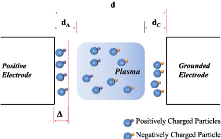
change in potential of the positive electrode. (A) Profiles of voltage and current with millisecond scale in SDGs. (B) Increase of potential of positive electrode at spark relaxation time. ... 48 Figure 2.18. Schematic of electro-deposition of charged particles in a plasma
on the electrodes during spark discharge. ... 50 Figure 2.19. Characteristic of electro-deposition of charged particles. (A)
Electro-deposition of the charged particles with respect to the capacitance in the spark circuit. (B) Electro-deposition of the charged particles with respect to the mobility of the charged particles. (Assume E0 = 1E6 V/m) ... 52 Figure 2.20. Charge distribution of particles via RR-SDG with InSn alloy with
respect to electrical polarity with a gap distance of 2.5 mm, argon gas flow rate of 3.5 lpm and applied positive potential of 5 kV. ... 53 Figure 2.21. Charge distribution of particles via PP-SDG with InSn alloy with
respect to electrical polarity with a gap distance of 2.5 mm, argon gas flow rate of 3.5 lpm and applied positive potential of 5 kV. ... 54 Figure 3.1. Ion-Assisted Aerosol Lithography. (A) Schematic of the principle
xv
of IAAL (B) SEM image of patterns via IAAL (Adopted from Kim et al.
2006). ... 61 Figure 3.2. Limitation of IAAL method with respect to dielectric thickness on
a conducting substrate. (A-C) the Focusing effect of IAAL increases as dielectric thickness on a conducting substrate increases. (D) Distortion of electric field line with 8 μm thick dielectric destroys ion induced focusing lens and nanoparticles are no longer deposited on the substrate.
(Adopted from You et al.). ... 63 Figure 3.3. Schematic of focused patterning of charged particles on a non- conducting substrate. (Adopted from You et al. 2010). ... 64 Figure 3.4. Three critical factors for patterning on a non-conducting substrate
via the IAAL. (A) Surfactant modifying hydrophilicity of the surface of the substrate. (B) Nanoparticle focusing mask substituting PR pre- patterns and forming electrostatic focusing lens by ion accumulation for the IAAL. (C) Charged particles and droplets supplied via electrospray during deposition. ... 67 Figure 3.5. Schematic of experimental setup for the patterning... 68 Figure 3.6. Surfactant. (Nonylphenolethoxylates) ... 69 Figure 3.7. Fabrication procedure for silicon nitride mask used in the
experiment. ... 71 Figure 3.8. Schematic of charged particle deposition via electrospray of
conducting liquid on a substrate. ... 72 Figure 3.9. Schematic of experimental setup for checking connectivity. ... 76 Figure 3.10. Current measurement through the temporary conducting film. (A)
xvi
Schematic of experimental setup. (B) Current measured with respect to surface treatment of the substrate. ... 76 Figure 3.11. Patterns of PSL particles on the thick glass. (A) Optical image of
0.7 mm thick glass substrate. (B) SEM image of the silicon nitride mask having line type openings (C) 420 nm line patterns consisting of 30 nm- sized PSL particles. (Adopted from You et al. 2010) ... 77 Figure 3.12. Patterns of PSL particles on the flexible PET film. (A) Optical
image of 0.1 mm flexible PET fillm. (B) Photography of the epoxy mask (C) 10 m line patterns and 12 x 12 m2 consisting of 100 nm-sized PSL particles. (Adopted from You et al. 2010) ... 78 Figure 3.13. Patterning of a micro conducting wire with silver ink on the
Kapton film. (A) Schematic of experimental setup. (B) SEM image of the 8 μm wide conducting wire. (C) Voltage and current relation for the conducting wire and inset shows the epoxy mask used for patterning.
(Adopted from work with J. Lee) ... 80 Figure 3.14. Patterning of gold nanoparticles generated via spark discharge
generator on the PET film. (A) Schematic of experimental setup. (B) SEM image of the 270 nm line patterns. (C) 350 x 350 nm2 square patterns. ... 82 Figure 4.1. The Jablonski diagram displaying the energy states of a molecule.
(Adopted from Lichtman and Conchello, 2005) ... 90 Figure 4.2. The Organic Light Emitting Diode fabricated in the experiment.
(A) The schematic of the OLED configuration. (B) Molecular structure of Alq3 used as both emitting layer and electron transfer layer. (C)
xvii
Molecular structure of NPB. ... 92 Figure 4.3. Energy band diagram for the organic bylayer of OLED fabricated
in the experiment. (A) Energy band of the OLED without electrical potential. (B) Energy band bending of the OLED with electrical potential and the resultant recombination. ... 93 Figure. 4.4. Schematic of experimental equipment for gold nanoparticle
deposition in the middle of the NPB film of the OLED. ... 95 Figure 4.5. Control of the sizes of nanoparticles in spark discharge. (A) Size
control by changing capacitance in the circuit. (B) Size control by changing the flow rate of the carrier gas. ... 97 Figure 4.6. Gold nanoparticles generated by spark discharge generators with a
gap distance of 1 mm, N2 gas flow rate of 2 lpm and applied positive potential of 5kV. (A) TEM images of gold nanoparticles for PPSDG and RRSDG. (B) Mobility diameter based size distribution for both configurations. ... 99 Figure 4.7. Mobility diameter based size distribution with respect to the
capacitance in the electrical circuit. ... 100 Figure 4.8. Gold nanoparticles generated adjusting the capacitances of the
external capacitor. (A,D) TEM and SEM images of gold nanoparticles via the SDG with nitrogen flow rate of 2 lpm, resistance of 20 Mohm and capacitance of 2 nF. (B,E) TEM and SEM images of gold nanoparticles via the SDG with resistance of 10 Mohm and capacitance of 4 nF. (C,F) TEM and SEM images of gold nanoparticles via the SDG with resistance of 5 Mohm and capacitance of 8 nF. ... 101
xviii
Figure 4.9. Gold nanoparticles generated adjusting the flow rate of carrier gas.
(A) A TEM image (B) A SEM image (C) Mobility based size distribution of gold nanoparticles via the SDG with resistance of 20 Mohm and capacitance of 2 nF depending on nitrogen flow rate... 102 Figure 4.10. Characteristics of the OLED devices with respect to capacitance
in the electric circuit (A) Characteristics of current density versus voltage driving the device. (B) External quantum efficiency of the devices. ... 104 Figure 4.12. Characteristics of the OLED devices with respect to N2 flow rate.
(A) Characteristics of current density versus voltage driving the devices.
(B) External quantum efficiency of the devices. ... 105 Figure 4.12. Photoluminescence spectra of the OLEDs with the particles
deposited at the distance of 20 nm from the emitting layer and the OLED without the particles. Inset shows the schematic of photoluminescence measurement using excitation source wavelength of 430 nm. ... 107 Figure 4.13. Extinction and absorption in the NPB layer with gold
nanoparticles. (A) Extinction spectrum of gold nanoparticles deposited at the distance of 20 nm from the emitting layer in middle of the NPB layer.
(B) Calculated absorption of NPB layer with gold nanoparticles with respect to size of a gold particle. ... 110 Figure 4.14. Electric fields in the OLED with fully charged gold nanoparticles
and external potential of 7 V. (A) Electric fields in the OLED with 6 nm- sized gold nanoparticles at the distance of 20 nm from the emitting layer in middle of the NPB layer. (B) Electric fields in the OLED with 10 nm- sized gold nanoparticles at the same position as the case of 6 nm-sized
xix
particles. (C) Electric fields at cathode and anode with respect to particle sizes comparing to the case without the particles. ... 111
xx
This page is intended to be blank
1
Chapter 1.
Introduction
2
1.1. Background of Research
Nanoparticle patterning has been widely studied as one of the promising alternatives to photolithography. Many researches on the patterning have been dealt with nanoparticles dispersed in aqueous or organic solvents with stabilization by surfactants (Liao et al. 2012; Son et al. 2011; Sung et al.
2012). Those nanoparticles are synthesized in various chemical ways in liquid but have inherent impurities such as stabilizers or surfactants accompanying by their production process. Various liquid-based patterning technologies, such as micro transfer molding, micro-molding, micro contact printing and nanoimprinting, represented by “Soft Lithography” have shown possibility and various applications. (Duan et al. 2010; Park et al.
2008; Wang et al. 2009) On the other side, gas phase particle synthesises also have been developed with advantages in terms of pure particle generation without impurities (Biskos et al. 2008; Borra 2006; Kruis et al.
1998). Gas-phase synthesized particles have been exploited for nanoparticle patterning by controlling the behavior of nanoparticles with electrical field (Krinke et al. 2002; Sung et al. 2012; Wang et al. 2009). Parallel and high resolution nanoparticle focused patterning with ion-induced electric field has been studied with aerosol technology (Kim et al. 2006; Lee et al. 2010;
You et al. 2010). Ion-assisted aerosol lithography (IAAL) is the focused pattering of charged particles using electrostatic lens formed by ion accumulation on the dielectric surface like a photoresist, which can guide and control the particle into wanted position.
3
Nanoparticle patterning via IAAL has significant prerequisites, which are composed of a number of charged particles, conductive substrates neutralizing incoming charged particles, ions for building electrostatic lens, and pre-patterned dielectric surface for ion accumulation and guidance of nanoparticles. Therefore, preparation of charged particles is one of the significant factors of IAAL. Charged particle generation has two distinct process composed of particle generation and particle charging (Borra 2006;
2008). A lot of particle generation methods have been reported but particle charging is not as numerous as particle generation. Diffusion charging and field charging are accomplished through high electric field or residence in plentiful ion clouds for suitable time, respectively (Borra 2008; Hinds 1999).
Electro-hydrodynamic atomization easily prepares charged particles from particles dispersed in conducting solvents (Cloupeau and Prunetfoch 1994;
La Mora and Fernandez 1994; Lenggoro et al. 2002). Conducting solvent, material stabilization in liquids, and relatively resultant large agglomerate of particles could limit the advantages of electrospray method. In addition, electrospray is not easy to be applied to the non-conducting liquids in which many liquid processed nanoparticles are dispersed under stabilization by surfactants.
Electrical discharges have been exploited to generate nanoparticles and their aggregates, and to deposit films on substrates, as shown in Fig. 1.1.
Spark discharge (Byeon et al 2008; Helsper et al. 1993; Roth et al. 2004;
Schwyn et al. 1988; Tabrizi et al. 2009) could be a good candidate method
4
for generating charged nanoparticles for aerosol patterning, which has simultaneous particle generation and charging in the plasma formed during spark discharge. In addition, particles have narrower size distribution and their sizes could be controlled by parameters defining spark discharge (Tabrizi et al. 2009). Nanoparticles are easily generated via evaporation of electrode material by heat and ion sputtering during spark discharge.
However, the as-generated particles via a conventional rod-to-rod type spark discharge often tend to get agglomerates (Bau et al. 2010). The generation of unagglomerated charged particle at high concentration via spark discharge is highly desirable in order to broaden its applications in nanotechnology and to establish spark discharge as a robust method in gas phase particle synthesis.
Figure 1.1 Mechanisms of vapor and particle production (nucleation), growth, charging and transport in atmospheric pressure electrical discharge. (Adapted from Borra 2006)
5
Studies of charged particle generation via spark discharge have been rare even though spark discharge have been known to generate charged particles (Borra 2006; Tabrizi et al. 2009). Therefore, characteristics of charged particles generation via SDG are deserved to be investigated further.
Up to date, IAAL has been well utilized for multi-dimensional patterning on conducting substrates. The patterning limited to the conducting substrates could confine the potential of the methods. Patterning of those charged nanoparticles on the non-conducting substrates is essential for enlargement of application of the IAAL. Precise positioning and arrangement of nanoparticles on non-conducting substrates such as thick glass or flexible polymer film have been needed for the production of nano- electronics and cost-effective nanodevices. Charged particle patterning on non-conducting substrates via controlled electric field is a challenge because neutralization of incoming charged nanoparticles is essential for the successive patterning on the non-conducting substrates. Therefore, the patterning method applying IAAL to non-conducting substrates is needed to be developed.
Metal nanoparticles have been widely used to increase efficient of OLED with the principle of localized surface plasmon resonance (LSPR) (Fujiki et al. 2010; Tanaka et al. 2011), which have been extensively engineered to enhance efficiency of light emission or absorption in optic devices (Okamoto et al. 2004; Schuller et al. 2010) as well as for bio-sensing / imaging (Hutter and Fendler 2004) and Raman spectroscopy (Campion and Kambhampati
6
1998). Another interesting phenomenon for metal nanoparticles is charge trapping or charge blocking behavior in the OLED. (Li et al. 2008) Wet- processed gold nanoparticles have typically been utilized to enhance the emission efficiency of OLED. (Fujiki et al. 2010) Positioning the nanoparticles in the middle of the OLED is very important to optimize the LSPR effect or the charge trapping effect considering quenching effect of metal particles. However, wet-processed metal nanoparticles are difficult to be deposited on organic materials without contamination or damage to them.
Aerosol based metal nanoparticles could be applicable to any position in the OLED devices without any stabilizer or surfactant. Especially, the spark discharge generator was used positioning them at desired positions in middle of the organic materials with a facile way and engineering the optimum position for maximizing the efficiency of OLED (Sung, H et al 2012). The influence of the sizes of metal nanoparticles on the emission efficiency of OLED at a known optimum position is needed to study further in order to find out the optimum size at the optimum position because spark discharge can easily control their sizes with spark parameters
In this study, we developed an unconventional type spark discharge generator for producing less agglomerated nanoparticles. Nanoparticles via the generator could be exploited as precise building block for the IAAL.
Also, we obtained focused patterning of spark generated particle on a non- conducting substrate by forming temporary conducting liquid film, which follows principal concepts of the IAAL and enables high resolution
7
patterning on the non-conducting substrate. Lastly, nanoparticles via the generator were applied to increase the efficiency of the OLED and their effects on the emission enhancement of the OLED were studied.
8
1.2. Objectives for Research
In this research, we pursue developing an efficient generation method of charged nanoparticles used as building blocks and eliminating the restriction of the IAAL for non-conducting substrates. To realize the goals, we develop a facile spark generator for less agglomerated and charged nanoparticles.
Next, we conceived a conducting path for charge neutralization on the surface of the non-conducting substrate. Also, we found another application utilizing those nanoparticles.
First, preparation of unagglomerated charged particles is one of essential factors for aerosol based nanoparticle patterning. Particle generation via spark discharge satisfies the need in a facile way because the generation and charging of those nanoparticles are accomplished via spark discharge, simultaneously.
Second, charged particle patterning on a non-conducting substrate have been still challenging unless charge neutralization and prevention of resultant repulsion between particles with same polarity are prepared. We proposed the temporary path to eliminate the charges from incoming charged particles by forming the conductive liquid film on the substrate.
Finally, those unagglomerated metal particles would be exploited to enhance the emission efficiency of electroluminescence devices utilizing charge carrier trapping or blocking behavior by the particles.
9
1.3. Scope of Research
Unagglomerated charged particles were obtained through an unconventional electrode type spark discharge generator, and focused patterning of charged nanoparticles was realized on non-conducting substrates utilizing a temporary conducting liquid film. Those charged nanoparticles were utilized for optic devices using their unique electrical effects including localized surface plasmon resonance effect and charge trapping effect.
Generation of unagglomerated charged particles is a critical factor for precise aerosol based nanoparticle patterning. Particle production by spark discharge has been known as a facile and reliable method generating nanometer sized particles. However, a conventional rod-to-rod type spark discharge generator presents agglomerate of particles unless high flow rate of a carrier gas is supplied. We develop an unconventional type spark discharge generator for producing less agglomerated nanoparticles and compare it with a conventional type spark discharge generator in terms of sizes and charge distribution of the particles in chapter 2. Also, changes in charge distribution of particles via the rod-to-rod type generator were investigated.
For focused patterning of particles on a non-conducting substrate, we proposed the temporary path to eliminate the charges from incoming charged particles by forming the conductive liquid film on the substrate in chapter 3.
Formation of conductive liquid film on the substrate is based on hydrophilic
10
characteristic of the surface. We used a surfactant to change the hydrophobic into hydrophilic surface. The droplets of conducting liquids via elcectrospray were supplied and the droplets formed thin film on the hydrophilic surface.
Nano and micro scaled patterns were obtained with PolyStyrene Latex (PSL) particles via this method, and conducting micro wires with silver nanoinks were patterned with several micro-sized resolutions. Sub-micro scaled gold nanoparticle patterns also were realized with charged particles via spark discharge generator.
In chapter 4, we proposed application of those unagglomerated particles to the OLED to enhance its efficiency utilizing charge trapping behavior even though LSPR effect of the particles was not dominant. Organic LED was fabricated with NPB as a hole transfer layer and Alq3 for both light emitting layer and electron transfer layer. Gold nanoparticles via our spark discharge generator were easy to be placed at a known optimum position in the middle of organic layer in contrast with other nanoparticle fabrication method without damage of organic material. LSPR effect of gold nanoparticles near the emitting layer was considered and charge trapping effect of the metal particles was also studied qualitatively. The optical and electrical effects of those nanoparticles on external quantum efficiency were evaluated.
Finally, we summarize and conclude the results and discussion of this study in chapter 5.
11
1.4. References
Bau, S., Witschger, O., Gensdarmes, F., Thomas, D. and Borra, J. (2010).
Electrical properties of airborne nanoparticles produced by a commercial spark-discharge generator. Journal of Nanoparticle Research, 1-7.
Biskos, G., Vons, V., Yurteri, C. U. and Schmidt-Ott, A. (2008). Generation and sizing of particles for aerosol-based nanotechnology. KONA Powder Particle J, 26, 13-35.
Borra, J. (2006). Nucleation and aerosol processing in atmospheric pressure electrical discharges: powders production, coatings and filtration. Journal of Physics D: Applied Physics, 39, R19.
Borra, J. (2008). Charging of aerosol and nucleation in atmospheric pressure electrical discharges. Plasma Physics and Controlled Fusion, 50, 124036.
Byeon, J., Park, J., Yoon, K. and Hwang, J. (2008). Site-Selective Catalytic Surface Activation via Aerosol Nanoparticles for Use in Metal Micropatterning. Langmuir, 24, 5949-5954.
Campion, A., Kambhampati, P. (1998). Surface-enhanced Raman scattering.
Chemical Society Review, 27, 241.
Cloupeau, M. and Prunetfoch, B. (1994). Electrohydrodynamic spraying functioning modes – a critical review. Journal of Aerosol Science, 25, 1021- 1036.
Duan, X., Zhao, Y., Berenschot, E., Tas, N. R., Reinhoudt, D. N. and Huskens, J. (2010). Large Area Nanoscale Patterning of Functional Materials by Nanomolding in Capillaries. Advanced Functional Materials, 20, 2519-2526.
12
Fujiki, A., Uemura, T., Zettsu, N., Akai-Kasaya, M., Saito, A. and Kuwahara, Y. (2010). Enhanced fluorescence by surface plasmon coupling of Au nanoparticles in an organic electroluminescence diode. Applied Physics Letters, 96, 043307-043307-043303.
Hinds, W. C. (1999). Aerosol technology: properties, behavior, and measurement of airborne particles (2nd).
Hutter, E., Fendler, J. H. (2004). Exploitation of Localized Surface Plasmon Resonance. Advanced materials, 16, 1685.
Kim, H., Kim, J., Yang, H., Suh, J., Kim, T., Han, B., Kim, S., Kim, D. S., Pikhitsa, P. V. and Choi, M. (2006). Parallel patterning of nanoparticles via electrodynamic focusing of charged aerosols. Nature Nanotechnology, 1, 117-121.
Krinke, T. J., Deppert, K., Magnusson, M. H., Schmidt, F. and Fissan, H.
(2002). Microscopic aspects of the deposition of nanoparticles from the gas phase. Journal of Aerosol Science, 33, 1341-1359.
Kruis, F. E., Fissan, H. and Peled, A. (1998). Synthesis of nanoparticles in the gas phase for electronic, optical and magnetic applications - A review.
Journal of Aerosol Science, 29, 511-535.
La Mora, D. and Fernandez, J. (1994). The current emitted by highly conducting Taylor cones. Journal of Fluid Mechanics, 260, 155-184.
Lee, H., You, S., Pikhitsa, P. V., Kim, J., Kwon, S., Woo, C. G. and Choi, M.
(2010). Three-Dimensional Assembly of Nanoparticles from Charged Aerosols. Nano Letters, 11, 119-124.
Lenggoro, I. W., Xia, B., Okuyama, K. and de la Mora, J. F. (2002). Sizing of
13
colloidal nanoparticles by electrospray and differential mobility analyzer methods. Langmuir, 18, 4584-4591.
Li, W., Pan, S. and Rothberg, L. J. (2008). Emissive Efficiency Enhancement of Alq3 and Prospects for Plasmon-enhanced Organic Electroluminescence, Society of Photo-Optical Instrumentation Engineers, 703224.703221- 703224.703227.
Liao, J., Li, X., Wang, Y., Zhang, C., Sun, J., Duan, C., Chen, Q. and Peng, L.
(2012). Patterned Close Packed Nanoparticle Arrays with Controllable Dimensions and Precise Locations. Small.
Okamoto, K., Niki, I., Shvartser, A., Narukawa, Y., Mukai, T. and Scherer, A.
(2004). Surface-plasmon-enhanced light emitters based on InGaN quantum wells. Nature materials, 3, 601-605.
Park, I., Ko, S. H., Pan, H., Grigoropoulos, C. P., Pisano, A. P., Fréchet, J. M.
J., Lee, E. S. and Jeong, J. H. (2008). Nanoscale patterning and electronics on flexible substrate by direct nanoimprinting of metallic nanoparticles.
Advanced Materials, 20, 489-496.
Schuller, J. A., Barnard, E. S., Cai, W., Jun, Y. C., White, J. S. and Brongersma, M. L. (2010). Plasmonics for extreme light concentration and manipulation. Nature materials, 9, 193-204.
Son, Y., Yeo, J., Moon, H., Lim, T. W., Hong, S., Nam, K. H., Yoo, S., Grigoropoulos, C. P., Yang, D. Y. and Ko, S. H. (2011). Nanoscale Electronics: Digital Fabrication by Direct Femtosecond Laser Processing of Metal Nanoparticles. Advanced Materials.
Sung, H., Lee, J., Han, K., Kim, C. and Choi, M. (2012). , Quantun efficiency
14
enhacement in a gold nanoparticle-embeded organic light emitting device engineering the particle position. In preparation.
Sung, S. H., Yoon, H., Lim, J. and Char, K. (2012). Reusable Stamps for Printing Sub-100 nm Patterns of Functional Nanoparticles. Small.
Tanaka, T., Totoki, Y., Fujiki, A., Zettsu, N., Miyake, Y., Akai-Kasaya, M., Saito, A., Ogawa, T. and Kuwahara, Y. (2011). Enhanced Red-Light Emission by Local Plasmon Coupling of Au Nanorods in an Organic Light- Emitting Diode. Applied Physics Express, 4, 2105.
Wang, Y. H., Mirkin, C. A. and Park, S. J. (2009). Nanofabrication beyond electronics. ACS nano, 3, 1049-1056.
You, S., Han, K., Kim, H., Lee, H., Woo, C. G., Jeong, C., Nam, W. and Choi, M. (2010). Nanoparticle patterning: High-Resolution, Parallel Patterning of Nanoparticles via an Ion-Induced Focusing Mask. Small, 6, 2146-2152.
15
Chapter 2.
Charged Aerosol Generation via
Spark Discharge
16
2.1. Introduction
Charged nanoparticles have been widely used for bottom-up nanoparticle patterning with electric forces, and the generation of those particles is one of the important factors in the patterning. Spark discharge at atmosphere (Schwyn et al. 1988) is a facile and reliable method for generating nanometer-sized particles among various gas phase synthesis methods (Biskos et al. 2008; Kruis et al. 1998). The method has advantages generating charged aerosols with a simple set-up, which can be exploited to construct nanostructures via controlled electric field (Krinke et al. 2002;
Kim et al. 2006; Lee et al. 2011). Up to now, rod-to-rod type spark discharge generators (RR-SDG) shown in Fig. 2.1. have been widely studied, and the effects of its parameters have been well defined (Tabrizi et al. 2009a) In addition, it has been recently applied to synthesize bimetallic or mixed metallic nanoparticles synthesis (Byeon et al. 2008a; Tabrizi et al.
2009b; Tabrizi et al. 2010), and to grow nanowires (Messing et al. 2009). A point-to-grid configuration was studied to demonstrate that aerosol production by corona in clean gas at atmospheric pressure was related to the development of plasma filaments reaching the low-field electrode grid in streamer and spark discharge regimes for positive point discharge while aerosol generation occurred only in the spark regime with negative point discharge (Borra et al. 1998). Even though a spark discharge generator (SDG) is known to produce nanometer sized particles, charged aerosols less than 10 nm at high concentrations tend to get agglomerated due to the post-
17
discharge electrostatic agglomeration of bipolar nanoparticles resulting from post-discharge diffusion charging in bipolar ion clouds, which was studied by measuring post-spark ion density for the RR-SDG (Bau et al.
2010). Prevention of agglomeration and generation of a larger amount of smaller sized charged aerosols from this facile method could further strengthen its advantages and widen the range of applications.
Agglomeration of particles in a SDG could be lessened by controlling some operational parameters such as spark frequency, spark energy and flow rate of a carrier gas over about 10 lpm (Helsper et al. 1993; Schwyn et al. 1988; Tabrizi et al. 2009a). In different systems such as in furnace reactor and flame reactor, ions have been utilized for preventing agglomeration of particles (Nakaso et al. 2003; Jung et al. 2008).
Figure 2.1. A conventional spark discharge generator (Adopted from Schwyn et al. 1988.)
18
Motivated by these, we attempt to use a pin-to-plate type electrode configuration for generating much smaller and unagglomerated charged aerosols compared to the conventional RR-SDG. The pin-to-plate type spark discharge generator (PP-SDG) has asymmetric electrodes consisting of a pin with a sharp tip as a positive electrode and a grounded plate with a central exit hole. Size and charge distributions of particles for both the PP- SDG and the conventional RR-SDG were measured, and spark parameters and flow pattern for both cases were investigated to explain why the PP- SDG produces much smaller and less agglomerate charged aerosols with a narrower size distribution at higher concentrations than the conventional RR-SDG.
Charged distribution of particles via RR-SDG could be changed with respect to spark frequency. Particle losses to the electrodes and chamber walls have been known to affect charge distribution of as-produced particles. However, characterization for charged distribution of particles via SDGs with respect to spark parameters has been rarely studied. Charge distribution was studied with RR-SDG and investigated with measuring charged particles with respect to spark frequency and the polarity of applied potential. The higher spark frequency in the RR-SDG produced the larger ratio of positively charged particles to negatively charged ones.
19
2.2. Experimental Concept
2.2.1. Spark discharge
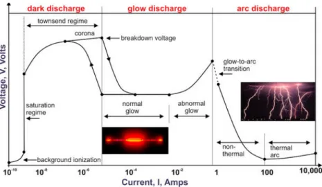
Spark is a transient electrical discharge phenomenon. Electrical discharge regimes are usually divided by dark discharge, glow discharge, and arc discharge, as shown in Fig. 2.2. These regimes could be classified by the value of current and the corresponding voltage lasting during electrical discharge. Current range of the dark discharge, glow discharge and arc discharge correspond to ~ μA with high voltage, ~ mA with moderate voltage, and above 1 A with relatively low voltages, respectively. The spark discharge with instantaneous current comparable to that of arc discharge could be called current limited arc or transient arc even though the spark is a transient discharge phenomenon different from these discharges. The state of the plasma in the channel of even a very transient spark discharge resembles the state in the arc column, so the spark discharge can be described as a pulsed arc (Raizer 1991). Spark discharge mechanism is normally explained by two discharge concepts. The Townsend model is based on self sustained electron multiplication by secondary electrons generated at an electrode. Paschen’s law has been satisfactorily used to estimate the breakdown criteria using the Townsend model. However, Townsend model is difficult to fully explain the discharge with large electrode gap, with the cathode material having very low secondary emission coefficient, and with asymmetric electric field and so on. To explain these discrepancies of Townsend model, a streamer concept was devised by Loeb, Meek and Raether, which is described as a thin ionized
20
channel between electrodes. The streamer is initiated by an electron avalanche like the Townsend model and then the streamer grows along the positively charged ions left by the initial avalanche. These avalanches are sustained by newly generated electrons close to streamers, and the electrons are produced by photons emitted from atoms excited by the primary and secondary avalanches. In this concept, the photons emitted from the atoms play critical roles in sustaining and growing the steamer. This concept is significantly different from Townsend model sustaining electron multiplication by secondary electrons. The streamer consisting of charges and having the resultant conductivity can connect both electrodes when it reaches the other electrode from one electrode. Consequently, electrical current may be sharply increased, which leads to a spark discharge between the electrodes.
Figure 2.2. Characteristic of Voltage and current during discharge (Adopted from http://www.plasma-universe.com)
21
2.2.2. Pin-to-Plate type spark discharge generator
The schematics of spark discharge chambers with two different electrode configurations used in the experiment; “pin-to-plate configuration” and
“rod-to-rod configuration” are depicted in Fig. 2.3. The configuration shown in Fig. 2.3A has asymmetric electrodes and the one shown in Fig.
2.3B has symmetric electrodes as used in a conventional SDG.
Figure 2.3. Two different configurations of spark discharge generator. (A) pin-to-plate type electrode configuration. (B) rod-to-rod type electrode configuration. (Adopted from Han et al. 2012)
22
Both generators are composed of a chamber having about 98.2 cm3 in volume with an inner diameter of 5 cm and height of 5 cm. For the pin-to- plate configuration, a pin electrode of diameter of 7mm was made to have a sharp tip with a radius of curvature of approximately 0.13 mm at the end with high positive potential while the grounded plate electrode was made to have an exit hole of 1-mm-diameter in the center. For the rod-to-rod configuration, two cylinders of electrodes having a diameter of 7mm are installed in the middle of the chamber. The electrode holders were precisely machined and assembled to the center position of the chamber to make sure accurate alignment within several micrometer tolerances. In-Sn alloy, silver and copper materials were prepared as electrodes and the gap distance between electrodes was fixed as 2.5 mm for both configurations. Argon gas with a purity of 99.999 % was used as a carrier gas with a fixed flow rate of 3.5 lpm. Generated particles were flowed out through the 1-mm-diameter exit hole for both cases. Experimental conditions were kept constant through all experiments.
23
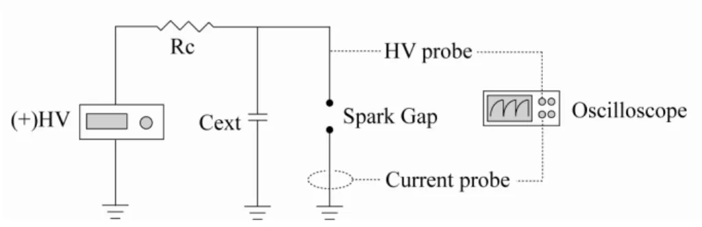
2.2.3. Electric circuit for spark discharge
The electric circuit for spark discharge was prepared similar to that widely used in other researches, as shown in Fig. 2.4 (Schwyn et al. 1988; Tabrizi et al. 2009a). The circuit was composed of a high voltage source (HV), an external capacitor (Cext) and a resistor (Rc). Charging current to the capacitor could be controlled by changing resistance of the charging resistor or the applied positive potential of the HV. The HV (Bertan 205B, maximum voltage of 10kV) was connected in serial through the charging resistor of 10 Mohm to the pin electrode for pin-to-plate configuration or one rod electrode for rod-to-rod configuration. The capacitor of 8 nF was connected in parallel to electrode which value is much larger than the intrinsic capacitance of SDGs measured as sub-pico Farad. A high voltage probe (HV probe) and a current probe were installed at positive electrode and a grounded cable, respectively in order to measure spark frequency and discharge current during spark.
Figure 2.4. Schematic of electric circuit for spark discharge system (Adopted from Han et al. 2012)
24
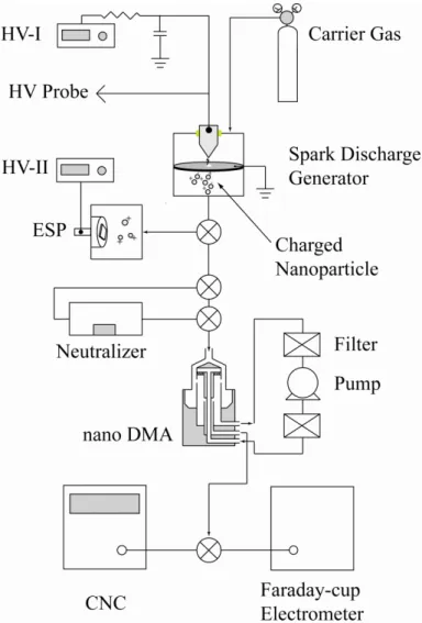
2.2.4. Measurement of sizes and charge distribution of particles The experimental setup for size measurements consists of differential mobility analyzer (DMA), condensation nuclei counter (CNC), Faraday-cup electrometer and electrostatic precipitator (ESP), as shown in Fig. 2.5.
Sampled particles for high resolution-transmission electron microscope (HR- TEM, JEOL JEM-3011) measurement were acquired on a TEM grid installed in ESP to observe the morphology and size of nanoparticles. Size distributions of generated particles based on electrical mobility diameter were measured by SMPS system composed of aerosol neutralizer (Kr-85), DMA (DS Industry, Column length of 15cm) and CNC (TSI 3022A). Size measurement for particles smaller than 5 nm was done with high resolution TEM image analysis and represented as projected area equivalent diameters (PAED). Particles were transported directly to DMA and the electrometer without passing through a neutralizer in order to measure currents for estimating the amount of charged aerosols having each polarity. Electrical mobility (Zp) of particles (Hinds, W. C. 1999) is defined in [Equation 2.1].
3
c p
p
Z neC
d
[Equation 2.1]
where n is the number of elementary charges of particles, e is the elementary charge, μ is dynamic viscosity of the carrier gas and dp is the
25
particle diameter, and Cc is the slip correction factor or Cunningham correction factor (Li and Chen 2005) defined as [Equation 2.2].
1 [1.142 0.558 exp( 0.999 )]
2
p c
p
C d
d
[Equation 2.2]
where μ and λ are dynamic viscosity and mean free path of carrier gas, respectively and dp is a particle diameter. Electrical mobility could be calculated in term of parameters of DMA as expressed in [equation 2.3].
ln( / )
2
sh
p outter inner
Z Q R R
LV
[Equation 2.3]where Qsh is the flow rate of sheath gas supplied to DMA, Routter and Rinner
are the outer radius and inner radius of DMA column, respectively, L is the column length of DMA and V is the voltages applied to inner column of DMA. Voltages applied to DMA could be obtained from relation of [Equation 2.1] and [Equation 2.3] in order to attract particles with the corresponding electrical mobility as follow.
3 ln( / )
2
p sh
outter inner c
V d Q R R
neC L
[Equation 2.4]
Size distribution of aerosols was usually measured with air as a carrier gas using SMPS system. In this experiment, argon was used as the carrier gas.
The use of argon as carrier gas has some precaution in SMPS measurement
26
contrary to the case of air environment. First, dynamic viscosity and mean free path of argon should be considered to calculate electrical mobility because properties of argon are different from those of air. The properties in Table 2.1 were used for mobility calculation. These properties should be set in SMPS before measurement. Secondly, calibration of flow meter in DMA controller supplying sheath flow to DMA should be checked since flow meter usually is calibrated in terms of air environment. In some cases, pump for sheath flow in DMA controller could be severely damaged due to high loading by misleading control signal when it is used without calibration.
Table 2.1. Properties of gases at Standard Conditions: 294.3K, 1 atm (Schmid et al. 2002)
Carrier Gas Mean free path[m] Dynamic viscosity[PaS]
Argon 7.07E-8 2.236E-5
Air 6.67E-8 1.82E-5
27
Figure 2.5. Experimental schematic for particle measurement system.
28
2.3. Results and discussion
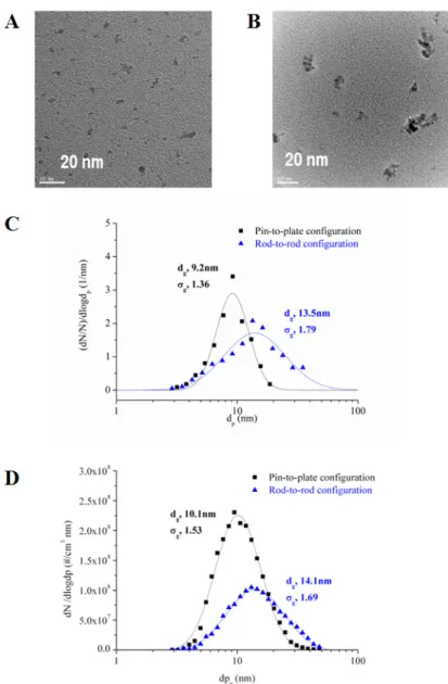
2.3.1. Less agglomerated aerosol via Spark Discharge
Figure 2.6 shows morphologies and size distributions of In-Sn alloy particles generated by each configuration with the applied positive potential of 5 kV. For PP-SDG, particles are less agglomerated than for RR-SDG, as shown in Fig. 2.6A and 2.6B. Size distributions were also compared from PAED size distributions based on TEM image analysis in Fig. 2.6C and mobility size distribution based on SMPS measurements in Fig. 2.6D. The geometric mean diameter (dg) of In-Sn alloy nanoparticles produced via the PP-SDG was found to be much smaller (PAED: 9.2 nm) than that via the RR-SDG (PAED: 13.5 nm), as shown in Fig. 2.6C. In addition, the PP-SDG generated particles having a narrower size distribution (geometric standard deviation, σg: 1.36) than that of the RR-SDG (σg: 1.79). Mobility size distributions measured by SMPS also shows the same trend in Fig. 2.6D.
Another interesting feature for the PP-SDG was that it produced more than twice the number concentrations of particles via the RR-SDG, as shown in Fig. 2.6D.
29
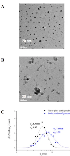
Figure 2.6. In-Sn alloy nanoparticles generated by spark discharge generator with a gap distance of 2.5 mm, argon gas flow rate of 3.5 lpm and applied positive potential of 5 kV. (A) A TEM image of particles for pin-to-plate type SDG. (B) A TEM image of particles for rod-to-rod type SDG (C) PAED based size distributions (D) Mobility diameter based size distributions. (Adopted from Han et al. 2012)
30
Generations of silver and copper nanoparticles were also examined via two different electrode configurations. Figure 2.7 and 2.8 show TEM images and PAED size distributions of silver and copper nanoparticles synthesized by each configuration with the same experimental conditions used for In-Sn alloy.
The same trend of achieving much smaller and unagglomerated nanoparticles was confirmed when the PP-SDG was used, as shown in Fig. 2.7A and 2.7B.
TEM analyses for silver and copper particles produced via two different electrode configurations show the generation of unagglomerated and smaller particles via PP-SDG compared to RR-SDG. The size distribution of silver particles with dg of 5.36 nm and σg of 1.37 for pin-to-plate configuration was obtained while conventional rod-to-rod configuration generated much larger nanoparticles with a broader distribution having dg of 7.19 nm and σg of 1.59 according to PAED analysis shown in Fig. 2.7C. The case of copper also demonstrated the same trend of generating smaller and narrower size distribution via PP-SDG as shown in Fig. 2.8A, 2.8B, and 2.8C.
31
Figure 2.7. Silver and copper nanoparticles generated by spark discharge with a gap distance of 2.5 mm, argon gas flow rate of 3.5 lpm and applied positive potential of 5 kV. (A) A TEM image of silver particles for pin-to-plate type SDG. (B) A TEM image of silver particles for rod-to-rod type SDG. (C) PAED based size distributions of silver particles. (Adopted from Han et al. 2012)
32
Figure 2.8. Silver and copper nanoparticles generated by spark discharge with a gap distance of 2.5 mm, argon gas flow rate of 3.5 lpm and applied positive potential of 5 kV. (A) A TEM image of copper particles for pin-to-plate type SDG. (B) A TEM image of copper particles for rod-to-rod type SDG. (C) PAED based size distributions of copper particles. (Adopted from Han et al. 2012)
33
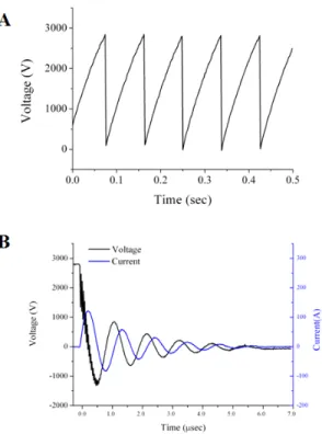
2.3.2. Electrical response during spark discharge
Electrical responses during spark discharge and charge states with respect to electrode configuration were obtained by monitoring voltage and current of the electrical circuit. Fluctuations of voltage and current during spark discharge are shown in Fig. 2.9. Both voltage and current during spark discharge oscillate symmetrically between their positive and negative values and decay within several μ-second.
Figure 2.9. Electrical responses during spark discharge. (A) Voltage oscillation with respect to time defining spark frequency (B) Voltage and current oscillation during spark discharge. (Adopted from Han et al.
2012)
34
2.3.3. Charge distribution of generated particles
The charge distribution of particles was obtained through measurement of the portion of each polarity aerosols generated from two different electrode configurations. Figure 2.10 shows measured current versus electrical mobility for positively and negatively charged particles of In-Sn alloy with applied positive potential of 5 kV. The PP-SDG produced about twice as much as the amounts of charged particles via the RR-SDG. In addition, the number of positively charged particles was approximately the same as that of negatively charged ones while unequal distribution of charged particles was obtained via conventional RR-SDG. Even though PP-SDG could generate unipolar positive ions between sparks, it seems that this could not influence charge distributions of particles significantly, since the faster transport of as- generated particles through the center hole could not allow sufficient time of charging. Contrastively, RR-SDG generated biased charge distributions:
more negative particles than positive ones.
35
Figure 2.10. Current versus electrical mobility for positively and negatively charged particles of In-Sn alloy for each configuration with a gap distance of 2.5 mm, argon gas flow rate of 3.5 lpm and applied positive potential of 5 kV. (Adopted from Han et al. 2012)
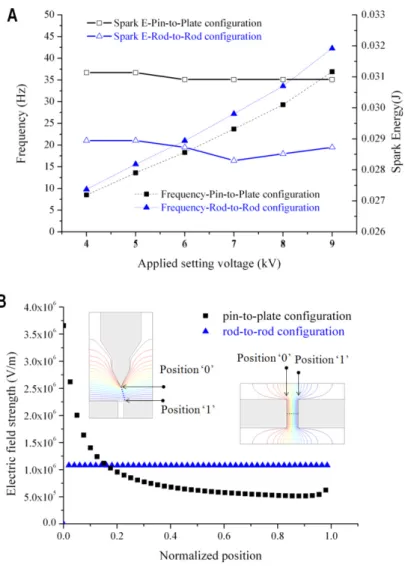
36 2.3.4. Spark parameter analysis
To explain why the PP-SDG generates much smaller and less- agglomerated nanoparticles with a narrower distribution than conventional RR-SDG, spark frequencies and spark discharge voltages were measured because the spark frequency is known to play an important role determining particle sizes (Tabrizi et al. 2009a). The spark discharge started to occur at the voltage of about 2.8 kV for PP-SDG and at about 2.7 kV for RR-SDG, respectively. Spark energy was calculated by the half of the product of the capacitance and the square of spark discharge voltage (Horvath and Gangl 2003). The spark frequency and spark energy versus applied positive potentials for two different configurations are presented in Fig. 2.11A. The PP-SDG has about 13% lower spark frequency and has about 7 % higher spark energy due to higher discharge voltage compared to the RR-SDG for fixed capacitance, electrode gap and applied potential of 5kV. The reason why the use of pin electrode decreases spark frequency and increases spark discharge voltage could be inferred from electric field analysis. Calculated electrical fields between electrodes by COMSOL software are presented in Fig. 2.11B and inset images describe the calculated equi-potential lines between the electrodes at the breakdown potential of 2.7 kV for the RR- SDG. Breakdown at the potential of 2.7kV with gap distance of 2.5mm for RR-SDG under Argon atmosphere seems to be reasonably compared with other reports (Tabrizi et al. 2009a; Vons, V. et al. 2011). Corresponding electric field strength for breakdown is calculated to be about 1E6 V/m.
37
Figure 2.11. Spark parameters and electric field strength for each configuration (A) Spark energy and spark frequency versus applied positive potentials for different configurations (B) the calculated electrical field strength between the gap of electrodes and equi-potential lines (insets) between the electrodes along the dashed lines for different configurations with the applied positive potential of 2.7 kV. (Adopted from Han et al. 2012)
38
Spark discharge in the PP-SDG began to occur at 2.8kV while the calculated electrical field strength near the plate was lower than the breakdown field strength. This discrepancy could be explained by considering space charges and reduced electric field which is defined by electric field divided by the density of neutral species (E/N) (Bau et al.
2010). Space charges including ions and electrons are generated at the end of sharp electrode near the discharge voltage by positive corona and streamers. Streamer can be changed into spark through the increase of reduced electric field caused by enhancement of ionization and the resultant decrease of neutral gases. Thus, the actual breakdown field strength may be lower than the numerically estimated value (Borra, 2006). This analysis explains qualitatively why the PP-SDG requires higher discharge voltage and thereby operates lower spark frequencies for the given applied positive potential compared to the RR-SDG. In addition, the radius of the curvature of the pin electrode could affect the electric field strength between the electrodes as shown in Fig. 2.12. However, the spark energy and spark period (inverse of spark frequency) are expected to decrease as the radius of curvature of pin electrode increases since the pin electrode having large radius of curvature behaves like a rod electrode. The effect of sharpness of pin electrode is hard to conclude because the sharper pin electrode has both higher spark energy and lower spark frequency under fixed applied setting potential in comparison to more blunted pin electrode. Difference in spark frequency and in its inversely proportional spark energy cannot explain fully the observed significant reduction of particle size and the phenomenon
39 of unagglomeration.
Figure 2.12. The calculated electrical field strength between the electrodes with respect to the radius of curvature of pin electrode for pin-to-plate electrode with the same condition as Fig. 2.11B
40
2.3.5. Flow pattern in spark discharge generators
Flow patterns should be significantly different for PP-SDG and RR-SDG due to totally different electrode geometry, i.e. transverse flow exists between electrode gap of RR-SDG and axial flow is dominant between gap of PP-SDG. Flow patterns both in PP and RR spark discharge generators (SDG) were studied using 3D model of commercial software, COMSOL and found to be very important. Red colored is the region of high velocity exceeding 3 m/sec. The calculations show that the PP-SDG has much higher gas velocity near particle generation zone and thus much faster transport of as-generated particles as shown in Fig. 2.13A than for the case of RR-SDG shown in Fig. 2.13B. This much faster transport of generated particles in the PP-SDG could reduce coagulation probability explaining both the generation of smaller sizes and less agglomeration than the case of the RR-SDG.
To find out whether the use of a pin electrode or flow pattern plays more dominant role on the reduction of coagulation probability for pin-to-plate type chamber, we studied an additional case of Pin to Rod (PR) type chamber in which one of the rods of the conventional RR-SDG was replaced by a pin electrode, as shown in Fig. 2.14A. The PR-SDG is expected to have the same characteristics of ion generation as the PP-SDG due to the use of the pin electrode while the flow pattern and resultant residence time would be similar to that of the RR-SDG. As shown in Fig.
2.14B, both the PR-SDG and the PP-SDG generated higher concentration of charged aerosols than the RR-SDG.
41
Figure 2.13 Flow fields near particle generation and coagulation zone for each configuration. Insets show colour plots of velocities up to 3 m/s emphasizing high velocities (red colour) between electrode gap of PP- SDG and low velocities (blue colour) between electrode gap of RR-SDG (A) Velocity and its contour in cross-sectional view (inset) near particle generation zone for pin-to-plate configuration. (B) Velocity and its contour in cross-sectional view (inset) near particle generation and coagulation zone for rod-to-rod configuration. (Adopted from Han et al.
2012)
42
It is clear that the use of the sharp pin electrode for both the PR-SDG and the PP-SDG could generate higher concentration of charged aerosols than the RR-SDG.
Figure 2.14. Pin-to-Rod type electrode configuration and charged particle generation during spark discharge with silver. (A) Pin-to-rod type electrode configuration. (B) Current versus electrical mobility for positively and negatively charged particles of silver for three different types of configuration with a gap distance of 2.5 mm, argon gas flow rate of 3.5 lpm and applied positive potential of 5 kV. (Adopted from Han et al. 2012)