저작자표시-비영리-변경금지 2.0 대한민국 이용자는 아래의 조건을 따르는 경우에 한하여 자유롭게
l 이 저작물을 복제, 배포, 전송, 전시, 공연 및 방송할 수 있습니다. 다음과 같은 조건을 따라야 합니다:
l 귀하는, 이 저작물의 재이용이나 배포의 경우, 이 저작물에 적용된 이용허락조건 을 명확하게 나타내어야 합니다.
l 저작권자로부터 별도의 허가를 받으면 이러한 조건들은 적용되지 않습니다.
저작권법에 따른 이용자의 권리는 위의 내용에 의하여 영향을 받지 않습니다. 이것은 이용허락규약(Legal Code)을 이해하기 쉽게 요약한 것입니다.
Disclaimer
저작자표시. 귀하는 원저작자를 표시하여야 합니다.
비영리. 귀하는 이 저작물을 영리 목적으로 이용할 수 없습니다.
변경금지. 귀하는 이 저작물을 개작, 변형 또는 가공할 수 없습니다.
Highly efficient deep-blue organic light emitting diodes utilizing triplet
exciton harvesting strategies
삼중항 여기자 수확 전략을 활용한 고효율 진청색 유기발광소자
2020 년 8 월
서울대학교 대학원 재료공학 전공
임 형 철
i
Abstract
Highly efficient deep-blue organic light emitting diodes utilizing triplet
exciton harvesting strategies
Hyoungcheol Lim Department of Materials Science and Engineering The Graduate School Seoul National University
OLEDs have been commercialized in mobile display as well as flexible or large-area displays because they have various advantages such as high color gamut and light weight. In addition, OLEDs have been applied to lighting products because they can be fabricated as a surface or flexible light source, and have high color temperature and color rendering index. For several decades, the development of various emitters such as phosphorescence and TADF materials has enabled the production of highly efficient OLEDs and contributed to the commercialization of OLEDs. However, in order for OLED to become
ii
more widely available in the future, more development and research must be conducted to increase the efficiency and color purity of blue OLED. In this research, triplet harvesting methods were explored and the efficient deep-blue OLEDs were developed.
In chapter 2, the high T1 exciplex host suitable for deep-blue phosphorescent OLEDs (phOLEDs) is introduced. The exciplex hosts for deep- blue OLEDs had not been reported at that time because of the difficulties in identifying suitable molecules. A deep-blue-emitting exciplex system with an exciplex energy of 3.0 eV is developed based on the molecular property analysis. And the exciplex system is applied to the deep-blue phosphorescent OLEDs. The blue PhOLEDs exhibited maximum external quantum efficiency of 24% with CIE color coordinates of (0.15, 0.21) and longer lifetime than the single host devices.
In chapter3, thermally activated delayed fluorescent (TADF) emitters with narrow blue emission spectrum are introduced. Both emitters exhibit narrow emission spectra with the full width half maximum (FWHM) less than 65 nm due to the rigid donor and acceptor unit. Furthermore, long molecular structure along the transition dipole moment direction results in a high horizontal emitting dipole orientation ratio over 80%. By combining the effects, the OLED utilizing DBA-SAB as the emitter exhibits maximum EQE of 25.7%
and CIE coordinates of (0.144, 0.212). Moreover, even a higher efficiency deep blue TADF OLED with a maximum EQE of 28.2% and 1931 Commission
iii
Internationale de l'éclairage (CIE) coordinates of (0.142, 0.090) is realized.
In chapter 4, triplet-triplet annihilation process is studied and blue OLEDs with thin efficiency-enhancement layer (EEL) is developed. Insertion of a very thin EEL (3 nm) between the deep blue emitting layer (EML) and the electron transport layer enhanced the EQE of the blue device by 44% compared to the device without the EEL, resulting in an EQE of 7.9% and a current efficiency of 9.0 cd A−1 at 1000 cd m−2; the CIE coordinates of the emitting color were (0.13, 0.14). The transient electroluminescence showed that the efficiency enhancement originates from the triplet−triplet annihilation (TTA) process in the EEL, followed by energy transfer to the emitting dye in the EML.
.
Keywords: Deep-blue organic light-emitting diodes, phosphorescence, fluorescence, thermally activated delayed fluorescence, triplet-triplet annihilation, delayed fluorescence
Student Number: 2014-22529
iv
Contents
Abstract ... i
Contents ... iv
List of Tables ... vii
List of Figures ... viii
Introduction ... 1
1.1 Brief introduction to Organic Light-Emitting Diodes ... 1
1.2 Parameters that governs the efficiency of OLEDs ... 4
1.3 Strategies for harvesting triplet excitons ... 8
1.4 Challenges for realizing high-efficiency deep blue OLEDs ... 14
1.5 Outline of the thesis ... 15
An Exciplex Host for Deep-Blue Phosphorescent Organic Light-Emitting Diodes ... 17
2.1 Introduction ... 17
2.2 Experimental ... 19
2.3 Result and discussion ... 21
2.4 Conclusion ... 35
v
Highly efficient deep blue OLEDs using TADF emitter with narrow emission spectrum and high
horizontal emitting dipole orientation ... 36
3.1 Introduction ... 36
3.2 Experimental ... 39
3.3 Result and discussion ... 41
3.4 Conclusion ... 58
Enhanced Triplet−Triplet annihilation of Blue Fluorescent Organic Light-Emitting diodes by Generating Excitons in Trapped Charge-Free Regions . 59
4.1 Introduction ... 594.2 Experimental ... 62
4.3 Result and discussion ... 64
4.4 Conclusion ... 95
Summary and Conclusion ... 96
Bibliography ... 99
초 록 ... 114
CURRICULUM VITAE ... 118
vi
List of Publications ... 120
List of Presentations ... 121
vii
List of Tables
Table 2.1 Summarized performances of PhOLEDs with CIE ycoordinate close to 0.2. ... 27 Table 2.2 Turn-on voltage, EQE, PE, and CIE coordinates of the PhOLEDs. 28 Table 3.1 Photophysical properties and rate constants of TDBA-SAF and DBA- SAB. ... 49 Table 3.2 Summarized performances of OLEDs using TDBA-SAF and DBA- SAB and summary of reported deep-blue TADF OLED devices with CIE y ≤ 0.1 and EQEmax > 5%. ... 57 Table 4.1 Turn-on Voltage, EQE, CE, PE, and CIE Coordinates of the devices.
... 71
viii
List of Figures
Figure 1.1 a) Samsung Galaxy S20 with OLED display (Samsung electronics 2020). b) LG rollable display (LG Electronics 2020). c) Flexible OLED lighting (LG display 2020). ... 3 Figure 1.2 Triplet annihilation process (quintet state intermediate pair is fully dissociated to the two triplet excitons because of the higher quintet state energy than 2T1) ... 9 Figure 1.3 Schematic illustration for the methods to harvest triplet excitons in OLEDs... 13 Figure 2.1 The (a) chemical structures and (b) HOMO and LUMO levels of mCP, BM-A10, and FCNIr. T1 energies of mCP, BM-A10, and exciplex are compared in the bottom of panel b. (c) The absorption spectrum of FCNIr (dichloromethane solvent, 5 mol %) and normalized PL spectra of mCP, BM- A10, mCP:BM-A10 (1:1 molar ratio), and mCP:BM-A10:FCNIr films. (d) Transient PL intensity of mCP:BM-A10 film at 300 K. The red dashed lines are the fitting curve using a double exponential function. The inset shows transient PL intensities of mCP, BM-A10, and mCP:BMA10 films up to 50 ns. ... 22 Figure 2.2 (a) Experimentally obtained angle-dependent PL (open circles) and simulated PL (solid line) of a 30-nm-thick BM-A10:mCP:FCNIr (12wt%) film
ix
at 455 nm. (b) Simulated (dashed line) and experimentally obtained (contour plot) angle-dependent PL spectra of an mCP:BM-A10:FCNIr (12 wt%) film.
... 23 Figure 2.3 (a) Current density−voltage−luminance characteristics of the single host and exciplex host-based devices. (b) The EQEs and PEs of the devices as a function of current density. The devices have the same structure except for the host materials, and the thickness of n-BM-A10 was 20 nm. (c) Relative luminance decay curves of devices at the initial luminance of 400 cd m−2. (d) Calculated and experimentally measured EQEs of the blue PhOLEDs. ... 25 Figure 2.4 (a) JVL characteristics of the devices. (b) The EQEs and PEs of the devices. (c) Normalized EL spectra of devices with various thicknesses of the BM-A10 layer. ... 29 Figure 2.5 (a) Current density−voltage (J−V) characteristics of the hole and the electron only devices. (Open symbols: measured data, solid lines: fitted by space charge limited current (SCLC) model) (b) The hole mobilities of mCP and mCP:BM-A10:FCNIr mixed films, as well as the electron mobilities of BM-A10 and mCP:BM-A10:FCNIr mixed films. (Open symbols: Extracted from the J−V characteristics. Solid lines: Fitted by Poole-Frenkel model.)... 34 Figure 3.1 (a) Calculated LUMO level of acceptor units and HOMO levels of donor units. (Gaussian 09, B3LYP/6-31G(d)) (b) Calculated natural transition orbitals (NTOs) of TDBA-SAF and DBA-SAB for 1,3CT and 3LE states. NTO
x
calculations were performed using optimized geometry of each excited states.
(1,3CT optimization: Gaussian 09, 6-31G (d,p)/CAM-B3LYP, 3LE optimization:
Gaussian 09, 6-31G (d,p)/M06-2X, 1,3CT single point energy: Jaguar, 6- 31G(d,p)/ωB97X-D (ω=0.1), 3LE single point energy: Jaguar, 6-31G (d,p)/M06-2X) ... 43 Figure 3.2 (a) The absorbance and photoluminescence (PL) spectra of TDBA- SAF and DBA-SAB in solution state. (b) Angle dependent PL (ADPL) intensity of p-polarized light from emitter doped DPEPO films. (c) Transient PL decay curves of emitter doped DPEPO films (inset: enlarged prompt decay curves).
... 45 Figure 3.3 The photoluminescence (PL) spectra of TDBA-SAF, DBA-SAB and TDBA-Ac in DPEPO host... 46 Figure 3.4 Cyclic voltammogram scans of solution, with methylene chloride, 0.1 M tetrabutylammonium hexafluorophosphate (TBAPF6) and 1mM TADF emitter. TBAPF6 was used as the supporting electrolyte. ... 47 Figure 3.5 (a) Prompt and delayed emission spectra at 300K (upper) and 100K (lower) of TDBA-SAF and DBA-SAB. (b) Phosphorescent emission spectra of TDBA, DBA, Triph-Trz. (c) 1CT, 3CT and 3LE state energy levels of TDBA- SAF and DBA-SAB. ... 52
xi
Figure 3.6 (a) Devices structure of OLEDs and molecular structures used in the device. (b) J–V–L characteristics (c) EQE plots and (d) EL emission spectra of devices. (inset in (b): simulated Lambertian emission patterns.) ... 55 Figure 3.7 Theoretically achievable EQE of devices as the thickness of TAPC and Bphen changes. ... 56 Figure 4.1 (a) Extinction coefficient of BD and PL emission spectra of BD, AP3Py-Na, AP3Py-2Na, ADP3Py and MADN films deposited on fused silica substrate. (b) Devices structure of OLEDs and (c) molecular structures used in the device. ... 66 Figure 4.2 Cyclic voltammetry scans of AP3Py-Na, AP3Py-2Na and ADP3Py (1 mM in dichloromethane with 0.1 M TBAHF6, scan rate of 100 mV s‒1). . 67 Figure 4.3 Experimentally obtained angle-dependent PL (open symbol) and simulated values (solid line) of a 30-nm-thick MADN:BD(5wt%) film. ... 68 Figure 4.4 (a) J-V-L characteristics, (b) EQE plots and (c) EL emission spectra of the devices. ... 70 Figure 4.5 Transient EL decay curves of device. Inset shows (EL intensity)-1/2 vs time. ... 74 Figure 4.6 Cyclic voltammetry results of MADN and BD (1 mM in dichloromethane with 0.1 M TBAHF6, scan rate of 100 mV s‒1). ... 76
xii
Figure 4.7 J-F curves of hole-only and electron-only devices of (a) 5wt% BD doped MADN and (c) EEL & ETL materials. (Solid lines: fitting lines in SCLC region using child’s law) Hole and electron mobility of (c) 5wt% BD doped MADN and (d) EEL & ETL materials. (Solid lines: fitting lines using Poole- Frenkel equation.) ... 78 Figure 4.8 Luminance vs current density characteristics of single layer electroluminescent devices. ... 80 Figure 4.9 Device properties as the thickness of ADP3Py layer changes. (a) EL emission spectra and (b) EQE plots. ... 82 Figure 4.10 EL emission spectra change of (a) non EEL device, (b) 3-nm-thcin ADP3Py used device, (c) 10-nm-thick ADP3Py used device as driving voltage increase. ... 83 Figure 4.11. Schematic illustration of TTA process in EEL considering ISC process from [TT]3 to S1. ... 88 Figure 4.12 Calculated Sn and Tn levels of ADP3Py (Gaussian 09, B3LYP/6- 31G(d)) ... 89 Figure 4.13 Calculated natural transition orbital (NTO) of ADP3Py ... 90 Figure 4.14 (a) Device structure using MBD 106 and M-tDABNA as emitter.
(b) Absorption and emission spectra of molecules used in the device. ... 91
xiii
Figure 4.15 (a) J-V-L characteristics, (b) EQE plots and (c) EL emission spectra of the devices. ... 92 Figure 4.16 (a) Transient EL results and (b) delayed emission ratio as the current density changes. (Orange lines in (a): fitted line by TTA model) ... 93 Figure 4.17 Analysis of efficiency composed of the EQE from prompt emission and TTA process of (a) MBD106 doped and (b) M-tDABNA doped device. 94
1
Introduction
1.1 Brief introduction to Organic Light-Emitting Diodes
In 1963, electroluminescence (EL) emission was observed from single crystal anthracene and tetracene doped anthracene by W. Helfrich and W. G.
Schneider.1 In 1987,C. W. Tang and S. A. Vanslyke reported the first bi-layered organic EL device and this device exhibited brightness of above 1,000 cd m-2.2 Since this discovery was reported, a lot of researches about organic light- emitting diodes (OLEDs) have been conducted intensively. More layers such as charge injection layer, charge transporting layer, exciton blocking layer and emitting layer (EML) have been added for improvements of efficiency and stability. Due to the different properties required for each layers, organic semiconductor materials have also been developed to meet the requirements.3–
6 Thanks to the much effort to improve the performance of OLEDs, OLED technologies are successfully commercialized in flat panel display and white lighting industry. (Figure 1.1)
Currently used OLEDs have multi-layered structure as explained above.
The organic layers are usually thermally deposited between metal electrodes.
Solution processes for OLED fabrication are also being studied because solution process is more efficient and cheap way for fabricating OLEDs. As an anode, transparent conducting film such as indium-tin oxide (ITO) is used that the light can come out of devices. The cathode electrode almost reflect the light
2
from EML. OLEDs can be fabricated on various substrates including flexible and transparent film, making rollable displays possible.
OLED market has been rapidly expanded in recent several years. OLED display have become dominant replace liquid crystal display (LCD) in small- sized displays and are beginning to be used in large area displays. Contrary to LCD, which were widely used as conventional displays, OLED panels do not require a light source due to their self-luminescent property. Therefore, OLED panels can be thinner and lighter compared with LCD. More importantly, OLED panels can control each pixel thus give high contrast ratio. Another advantages of OLED panels is low power consumption, high color purity, and fast repetition rate. Due to their advantages, OLEDs have been considered as a promising next-generation display, and are widely used as displays for various electronic devices. Also for a solid-state lighting, OLEDs have several advantages over conventional lightings. OLEDs are eco-friendly light source which have higher efficiency compared to light bulbs and incandescent lamp.
In addition, OLEDs have high color temperature and color rendering index (CRI), and they can be manufactured as a large-area and flexible surface light source.Therefore, OLEDs are expanding their applications not only in displays but also in lighting.
3
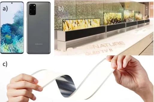
Figure 1.1 a) Samsung Galaxy S20 with OLED display (Samsung electronics 2020). b) LG rollable display (LG Electronics 2020). c) Flexible OLED lighting (LG display 2020).
4
1.2 Parameters that governs the efficiency of OLEDs
The externa quantum efficiency (EQE) of OLEDs has been expressed as follows:7–9
int out b rad eff out
EQE
q
(1.1)where
int is the internal quantum efficiency (IQE), and
out is the out-coupling efficiency of OLEDs.IQE can be expressed as the products of charge balance factor (
b), radiative exciton ratio (
rad) and effective photoluminescence (PL) quantum yield (qeff).
b expresses exciton formation efficiency, which means the ratio of generated excions to injected charge carrier. Thus
b is unity when the same number of injected holes and electrons are recombined in OLEDs. qeff expresses the radiative quantum yield of the emitter in a cavity structure. qeff depends on PLQY (
PL ) of emitter and can be reduced when the device is operating due to the exciton quenching by polarons.10
rad is the important factor influencing IQE of OLEDs. According to the spin-statistics, injected electrons and holes in OLEDs generate singlet and triplet excited states with a ratio of 1:3. The first-generation OLEDs were based on fluorescent emitters. Fluorescent emitters only utilize the singlet excited5
states for the light-emission process and the triplet excited states decay as non- radiative process. Therefore, maximum IQE of conventional fluorescent OLEDs was limited to 25%. If the 75% of triplet excitons are harvested to the radiative process, the efficiency of OLEDs can be improves significantly, so many researchers have developed the methods to utilize 75% of triplet excited states in light-emitting process. Details about triplet harvesting methods will be covered in Chapter 1.3.
Because qeff and
b can be improved with optimized device structures, the structure of OLEDs have been changed to achieve the high efficiency. When the distance between emitters is close enough for energy transfer, qeff is reduced because of the self-quenching. To reduce self- quenching of emitter, host-dopant system was introduced.11 An EML structure in which a small amount of emitter was doped into the host material was devised, which reduced the self-quenching due to the sufficient distance between the emitters. For the high
b values, charge imbalance have to be minimized. At low current density, low
b value can be explained by the difference in energy barriers for holes and electrons to be injected into the device. Therefore the efficient charge injection from electrodes is required.Many materials and technics for efficient charge injection to the OLEDs have been developed.12 One of the efficient methods to inject charge is electrical doping.13,14 Some transition metal oxides and alkali metal carbonates have been
6
used as p-type and n-type dopants for hole injection and electron injection, respectively.15–18 Injected charges have to recombine in EML for high efficiency because emitter is located in EML. To confine injected charges in EML, charge blocking layer have been adopted and the efficiency of OLEDs was enhanced.19 Also, mixed-host and bipolar host materials have been developed for balanced charge transport in EML.20,21
out depends on the emitting dipole orientation() of emitters in EML and this value can be enhanced when the emitters have horizontal dipole orientation.22–24 There was a report that maximum EQE of green OLEDs can increase around 26% to 46% without any light extraction structure when the value of emitter, which has photoluminescence (PL) quantum yield (PLQY) of 1, changes from 0.67 (random orientation) to 1 (fully horizontal oriented).9 In addition, OLEDs with maximum EQE over 40% can be realized in red and blue region when using the emitter has
PL=1 and =1.25,26 Many researches to achieve high have been conducted and some of them successfully increased the o u t of OLEDs by developing efficient and horizontally oriented emitters.27–29 Meanwhile, when the organic materials, which have low refractive indices, are used as transporting or host layer the o u t can be further increased due to the reduced substrate and wave-guided modes of OLEDs.30,31 If the organic materials constituting OLEDs have a low refractive index of 1.5, theoretically achievable maximum EQE is over 60%.32 Several efforts have been performed to increase the o u t through the development of organic7
materials with low refractive indices or design of device structure considering the refractive indices of materials.32,33
8
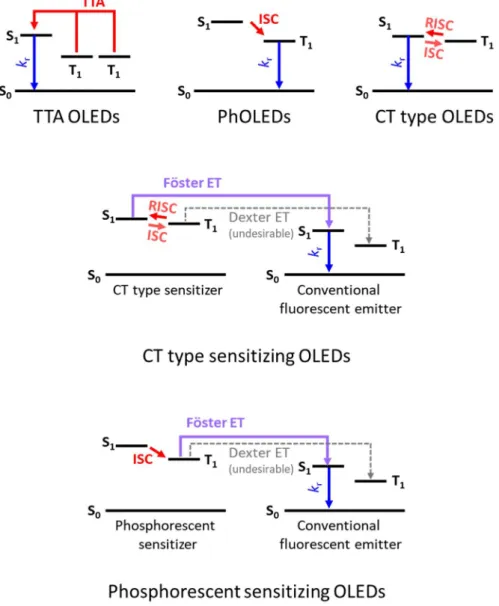
1.3 Strategies for harvesting triplet excitons
The
rad is one of the factors that can affect the efficiency of OLEDs, as described above. When only singlet excitons participate in radiative emission,
rad is 25% due to the spin statics. For higher efficiency of the OLEDs, non- radiative triplet exciton should be harvested to emissive radiation. A lot of efforts have been made to enhance
rad.Triplet-tripelt annihilation (TTA) by fluorescent molecules such as rubrene or anthracene and their derivatives is used to harvest the electrically generated triplet excitons, thereby the IQE of such OLEDs may exceed the spin statistical limit of 25%.34 The anthracene derivatives are usually used in blue emitting OLEDs and the TTA process can be expressed as in Figure 1.2. The annihilation of two triplet excitons leads to an intermediate state according to the spin statics (one singlet state, three triplet states and five quintet states). The lowest quintet state of anthracene monomer is not known but may be sufficiently high as to be inaccessible from the quintet intermediate state.35 Then quintet state intermediate states are fully dissociated to two triplet excitons and quintet intermediate state do not affect to TTA process.
9
Figure 1.2 Triplet annihilation process (quintet state intermediate pair is fully dissociated to the two triplet excitons because of the higher quintet state energy than 2T1)
10
Now we can consider eight triplet excitons which generates one singlet state pair and three triplet state pair. Each pair will decay to the lowest singlet and triplet state. As a consequence, five triplet excitons give one singlet exciton and the triplet harvesting ratio through TTA process is 20%. However, when the energy state satisfies T2>2T1, triplet intermediate pair will dissociate to two triplet excitons.36 In this case the maximum triplet harvesting efficiency from the TTA process is 50%, thus 37.5% of singlet excitons can be converted from the electrically generated triplet excitons. The theoretically achievable IQE of the OLEDs utilizing TTA process is considered to be 62.5%.36,37
In the late of 1990s, M. Baldo et al. reported novel emitters that contains heavy metal atom.38 Because the heavy metal induced large spin-orbit coupling (SOC), fast intersystem crossing (ISC) from singlet state to triplet state as well as from triplet state to ground state is possible. Thus, the emissive transition from triplet state to ground state, which is called phosphorescent emission, enables
rad of 100%. The OLEDs utilizing phosphorescent emtters, which are called phOLEDs, can achieve maximum IQE of 100% theoretically, significantly enhancing EQE of OLEDs.39–41 A lot of efficient red, green and blue emitting phosphorescent emitters have been developed and most of them contains iridium (Ir) or platinum (Pt) atoms.42–44Charge transfer (CT) type emitters can also give 100% of IQE by harvesting triplet excitons. CT type emitters have separated highet occupied molecular orbital (HOMO) and lowest occupied molecular orbital (LUMO).
11
The separated HOMO and LUMO minimizes electron exchange energy, resulting in small singlet-triplet energy level difference (ΔEST).45 Because of the small ΔEST, reverse intersystem crossing (RISC) process from triplet state to singlet state can be increased. Non-radiative triplet excitons can be harvested to the radiative singlet state by efficient RISC process. The excited state CT between two different molecules can be occurred and this molecular pair is called excited state charge transfer complex (exciplex).46,47 Intramolecular CT is also possible and the molecule exhibiting intramolecular CT is called thermally activated delayed fluorescent (TADF) material.48–50 Despite the emission is released from the singlet excitons, both exciplex and TADF emitters can theoretically achieve the maximum IQE of 100% via RISC process.
Because those CT type emitters do not contain heavy metal aoms, which are calssified as rare erth metal atoms, the cost for fabricating OLEDs can be saved as the CT type emitters are utilized.
The
rad can be enhanced with conventional fluorescent emitters, which do not harvest triplet exciton. When the emitter is introduced to the triplet harvesting material, energy transfer from the triplet harvesting material to emitter, following triplet exciton harvesting process.51–53 In this case, the light is released from the singlet exciton of conventionalf fluorescent, which have fast radiative decay lifetime (ns scale). Therefore, excitons can be cosumed very quickly and the exciton density in emitting layer (EL) can be lowered. As a results, the exciton-exciton quenching process, which brings about efficiency12
roll-off and degradation of OLEDs, can be reduced.
Schematic illustration of triplet harvesting OLEDs are presented in Figure 1.3
13
Figure 1.3 Schematic illustration for the methods to harvest triplet excitons in OLEDs.
14
1.4 Challenges for realizing high-efficiency deep blue OLEDs
The three principal color (red, green and blue) is required for the full- color OLED display. Among the three colors, blue-light-emitting materials and devices still need to be improved. The EQE of blue emitting devices is still inferior to that of the red and green devices and color purity also should be improved for large color gamut. Also it is well known that the power consumption of a full-color OLED is highly dependent upon the color purity of blue emission.54 The color purity can be expressed with a Commission Internationale de l’Éclairage (CIE) coordinates and the smaller CIE y-value, the lower the power consumption (lm W–1) of the device.
The main obstacle for the realization of high-efficiency deep-blue OLEDs is that only few materials can meet the requirements of deep blue emission, narrow FWHM, horizontally oriented and high PLQY properties.
Therefore, more studies on the material properties should be conducted.
15 1.5 Outline of the thesis
In this thesis, deep-blue OLEDs utilizing various triplet harvesting methods will be presented. Color purity and efficiency of phOLEDs were improved using newly developed high T1 exciplex system host. TADF OLEDs were developed that emits deep-blue using a TADF emitter with a narrow FWHM and a horizontally oriented emitting dipole moment. Also, highly bright and efficient blue fluorescent OLEDs were developed based on the understanding on the TTA process.
In chapter 2, it was verified the efficient blue phOLED can be fabricated using a deep-blue exciplex host. Using carbazole based donor and phosphine oxide based acceptor the deep-blue exciplex system was developed and used as a host system. The blue PhOLEDs doped with FCNIr achieved a turn-on voltage of 2.9 eV, a maximum EQE of 24% with CIE coordinates of (0.15, 0.21), and an EQE of 19% with CIE coordinates of (0.15, 0.19). Moreover, the exciplex host devices showed much better performances in EQE, power efficiency (PE), driving voltage, and operational lifetime than the single host devices.
In chapter 3, the analysis on the deep-blue TADF emitter was conducted.
The emitters have long molecular structure along the direction of transition dipole moment and contain oxygen-bridged acceptor unit, which is highly rigid.
A deep-blue OLED was fabricated using the TADF emitter, and it achieved EQE of 29.3% and CIE coordinate of (0.142, 0.090). The RISC mechanism was
16
analyzed using the electronic structures of emitter.
In chapter 4, TTA mechanism of anthracene based materials is analyzed.
The three new anthracene based materials were presented, which were used as efficiency enhancement layer in blue fluorescent OLEDs. The charge mobility of anthracene based materials was a key factor affecting triplet harvesting efficiency by TTA process. Insertion of a very thin EEL (3 nm) between the blue EML and the electron transport layer enhanced the EQE of the blue device by 44% compared to the device without the EEL, resulting in an EQE of 7.9%
and a current efficiency (CE) of 9.0 cd A−1 at 1000 cd m−2; the CIE coordinates of the emitting color were (0.13, 0.14). Interestingly, one materials showed delayed emission ratio above 40%, which is higher value than spin statistical limit of TTA process. Electronic structure and transition orbital analysis of the material was conducted. As a consequence, deep-blue fluorescent OLEDs with better characteristics in terms of efficiency roll-off property and color purity were developed. Deep-blue fluorescent OLED exhibited a maximum EQE of 8.8% and a maximum CE of 6.3 cd A-1, CIE coordinates of (0.136, 0.079). The maximum efficiencies were obtained at 5,000 cd m-2.
17
An Exciplex Host for Deep-Blue Phosphorescent Organic Light-Emitting Diodes
2.1 Introduction
The efficiency of OLEDs has improved significantly in recent years, largely because of improved device structures and new emitting materials with high PLQYs and horizontal emitting dipoles ratios (Θ).25,48,55–62 Device structures utilizing a mixed host forming an excited state charge transfer complex (exciplex) are particularly interesting for their high efficiencies approaching the theoretical limit, as well as low driving voltage and low- efficiency roll-off.32,63 A large number of high-efficiency OLEDs based on exciplex hosts have been reported using phosphorescent dyes, TADF dyes, and conventional fluorescent dyes for sky blue, green, yellow, and red colors.51,64–70 However, there have been rare reports of efficient OLEDs based on exciplex hosts for deep blue, that is, a CIE y-coordinate approaching or less than 0.2. An efficient exciplex host for an OLED requires a hole-transporting material (HTM) and an electron-transporting material (ETM), where the triplet (T1) energies of the constituent materials and the exciplex should be greater than the T1 energy of the emitting dopants.71 It is difficult to find host materials that satisfy these requirements for deep blue emission. Recently, exciplex system for deep blue phosphorescent OLEDs (phOLEDs) was reported.72 However, the efficiency is still much lower than red, green and sky blue phOLEDs.
18
Here, we report an exciplex-forming mixed host composed of N,N′- dicarbazolyl-3,5-benzene (mCP) as the HTM and 2,4-bis(4-(diphenyl- phosphoryl)phenyl)pyridine (BM-A10) as the ETM. Both molecules have T1
energies greater than 2.8 eV.73,74 The mixed layer forms an exciplex with an emission energy of 3.0 eV. Because the exciplex system has a small singlet−triplet energy difference (ΔEST), it satisfies the requirements for efficient blue PhOLED for tris((3,5-difluoro-4-cyanophenyl)-pyridine) iridium (FCNIr), where the T1 energy is 2.73 eV with the peak wavelength of 455 nm.
The fabricated devices exhibited a maximum EQE of 24% with CIE coordinates of (0.15, 0.21), and a turn-on voltage of 2.9 V. The efficiency is much higher than the recently reported OLEDs based on the different exciplex host from ours.
19 2.2 Experimental
Fabrication and PL Measurement of Organic Thin Films. Organic thin films were fabricated by thermal evaporation onto clean quartz substrates in a vacuum chamber (base pressure < 5 × 10⁻⁷ Torr). PL spectra were measured using a continuous-wave Xe lamp (300 nm) at room temperature. Transient PL was measured using an N2 laser (337 nm, Usho Optical Systems Co.) and a streak camera (Hamamatsu, C10627).
Fabrication of Hole-Only Devices (HOD), Electron-Only Devices (EOD), and Blue PhOLEDs. 150 nm-thick ITO substrates were used for the HOD and EOD devices, and 70 nm-thick ITO substrates were used for the PhOLEDs. These substrates were cleaned using acetone and boiling isopropyl alcohol. After they were dried in an oven at 80 °C, the ITO substrates were exposed to ultraviolet light and ozone. The organic layers and Al electrodes were then thermally evaporated in a vacuum chamber (base pressure <5 × 10⁻⁷ Torr). All devices were encapsulated in a glovebox following evaporation.
Measurement of Angle-Dependent PL and EL. Angle dependent p- polarized PL spectra were measured to determine the fraction of Θ, which was calculated using the classical dipole model. The emission patterns of the PhOLEDs were measured using an angle dependent EL setup. The experimental setup contained a motorized rotation stage, a programmable source meter (Keithley 2400), and a fiber optic spectrometer (Ocean Optics S2000).
20
Device Characterization. J−V−L and J−V characteristics were measured using a programmable source meter (Keithley 2400), and EL spectra were measured in the normal direction using spectrophotometer PR650 (Photo Research).
21 2.3 Result and discussion
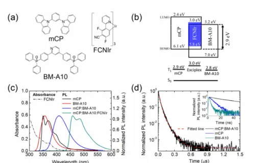
Figure 2.1a and b show the chemical structures and the highest occupied molecular orbital (HOMO) levels and the lowest unoccupied molecular orbital (LUMO) levels of mCP, BMA10, and FCNIr, respectively.57,66,73,74 Figure 2.1c shows the absorbance spectra of FCNIr and normalized photoluminescence (PL) spectra of mCP, BM-A10, an mCP:BM-A10 mixed layer (1:1 molar ratio), and mCP:BM-A10:FCNIr. Exciplex formation in the mCP:BM-A10 mixed layer is evidenced by the featureless broad emission spectrum, which is red-shifted from the constituent materials. The emission energy was 3.0 eV, which is close to the energy difference (2.9 eV) between the LUMO level of BM-A10 and the HOMO level of mCP. One must note that the T1 energy of the exciplex estimated from the peak position of the exciplex emission is higher than those of the constituting molecules of mCP and BM-A10 (Figure 2.1b).73,74 In other words, the T1 energy of the exciplex is not confined in this exciplex forming mixed host system as displayed in the bottom of Figure 2.1b. The PLQY of the exciplex emission was 0.17 and that of FCNIr doped in the exciplex was 0.82 as measured using an integrating sphere. The fraction of Θ of FCNIr in the exciplex host was 0.77 (Figure 2.2).
22
Figure 2.1 The (a) chemical structures and (b) HOMO and LUMO levels of mCP, BM-A10, and FCNIr. T1 energies of mCP, BM-A10, and exciplex are compared in the bottom of panel b. (c) The absorption spectrum of FCNIr (dichloromethane solvent, 5 mol %) and normalized PL spectra of mCP, BM- A10, mCP:BM-A10 (1:1 molar ratio), and mCP:BM-A10:FCNIr films. (d) Transient PL intensity of mCP:BM-A10 film at 300 K. The red dashed lines are the fitting curve using a double exponential function. The inset shows transient PL intensities of mCP, BM-A10, and mCP:BMA10 films up to 50 ns.
23
Figure 2.2 (a) Experimentally obtained angle-dependent PL (open circles) and simulated PL (solid line) of a 30-nm-thick BM-A10:mCP:FCNIr (12wt%) film at 455 nm. (b) Simulated (dashed line) and experimentally obtained (contour plot) angle-dependent PL spectra of an mCP:BM-A10:FCNIr (12 wt%) film.
24
The transient PL of the mCP:BM-A10 film is presented in Figure 2.1d and compared with those of the mCP and BM-A10 films (inset). It was well fitted with a double exponential curve with the excited state lifetimes of 26 and 86 ns, which are much longer than those of mCP or BM-A10. However, the lifetimes are much shorter than those of the delayed components of the normal transient PL of T1 confined exciplex systems where T1 of exciplex is lower than host T1’s.46,64 This relatively short decay time of the mCP:BM-A10 exciplex system is attributed to the weakened T1 harvesting of the exciplex with reverse intersystem crossing because the T1 energy of the exciplex is not confined. Also, T1 fusion can also contribute to the delayed emission as reported by Monkman et al.75
Blue PhOLEDs were fabricated via vacuum deposition. The structure of the devices is as follows: indium tin oxide (ITO) (70 nm)/6 wt % ReO3-doped mCP (30 nm)/mCP (20 nm)/emitting layer (EML, 30 nm)/BM-A10 (20 nm)/12 wt % Rb2CO3 doped BM-A10 (20 nm)/Al (100 nm). The EML was formed of an mCP:BM-A10 mixed film (1:1 molar ratio) doped with 12 wt % FCNIr. The thicknesses of the ETL (n-BM-A10 layer) were optimized in terms of efficiency and emission color. The devices based on the mCP and the BM-A10 single host were also fabricated with the same structure and the same doping concentration for comparison.
25
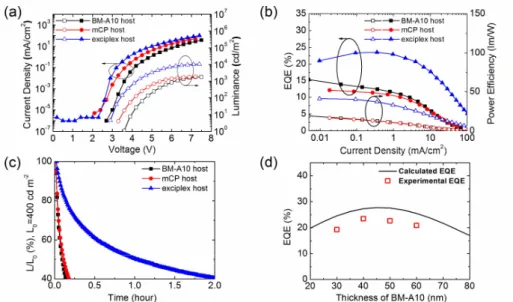
Figure 2.3 (a) Current density−voltage−luminance characteristics of the single host and exciplex host-based devices. (b) The EQEs and PEs of the devices as a function of current density. The devices have the same structure except for the host materials, and the thickness of n-BM-A10 was 20 nm. (c) Relative luminance decay curves of devices at the initial luminance of 400 cd m−2. (d) Calculated and experimentally measured EQEs of the blue PhOLEDs.
26
The device characteristics are compared in Figure 2.3. The exciplex host devices showed higher EQE, higher PE, lower driving voltage, and lower efficiency roll-off than the single host devices. The device with the exciplex host exhibited a maximum EQE of 24% and maximum power efficiency (PE) of 41 lm W−1 with a CIE y-coordinate of 0.21. The efficiencies are the highest among the devices reported up to now based on the FCNIr as the dopant to our best knowledge (Table 2.1).55,56,59,60,72,76–79 The turn-on voltage of the device using the exciplex host was the lowest with 2.9 V among the devices, probably due to the no injection barrier from the hole and electron transporting layers to the EML in the device. The device with a 10 nm-thick n-BM-A10 layer exhibited a little deeper blue color with a CIE y-coordinate of 0.19 at the expense of efficiencies with a maximum EQE of 19%, a maximum power efficiency (PE) of 33 lm W−1 (Figure 2.4). Table 2 lists a summary of the device characteristics. The CIE coordinates of the devices at the current density of 50 mA cm−2 are compared with those at the current density of 10 mA cm−2 in Table 2. The CIE y-coordinates of the OLEDs based on the BM-A10 single host changes by 0.02 (red shift) as the current density increases from 10 to 50 mA cm−2. In contrast, the CIE coordinates of the OLED based on the exciplex host at 50 mA cm−2 are similar to those at a current density of 10 mA cm−2, indicating that the recombination zone of the exciplex system does not shift much at high current densities even at 50 mA cm−2. This fact may be related to the lower efficiency roll-off and higher stability.
27
Table 2.1 Summarized performances of PhOLEDs with CIE ycoordinate close to 0.2.
Host Dopant Von [V] EQE [%]a) PE [lm W-1]a) CIE (x, y) Ref.
mCP:BM-A10
(exciplex) FCNIr 2.9 24 / 23 / 21 41 / 34 / 23 (0.15, 0.21) This work
t-DCDPA:DBFTrz
(exciplex) FCNIr 4.0 16.4 / – / 14.7 – / – / – (0.14, 0.20) 72
pBCb2Cz:TSPO1
(mixed) tBUCN-FIrmMes 3.0 22.4 / – / 22.4 31.9 / – / 24.9 (0.14, 0.21) 56
TSPO1 fac-Ir(pmp)3 4.0 10.1 / – / 9.0 – / – / – (0.16, 0.09)
TSPO1 mer-Ir(pmp)3 3.0 14.4 / – / 13.3 – / – / – (0.16, 0.15) 55
BCPO (fpmi)2Ir(dmpypz) 3.2 17.1 / 16.5 / 15.1 19.8 / 15.0 / 11.2 (0.13, 0.16) 76
PPO2 FCNIr – 18.4 / 13.5 / – 16.6 /9.1 / – (0.14, 0.15) 59
PPO21 FCNIr 3.5 20.4 / – / 11.9 26.1 / – / 6.6 (0.14, 0.19) 60
PO9 Ir(dbfmi) 2.6 18.6 / 13.6 / 6.2 35.9 / 19.6 / 6.3 (0.15, 0.19) 77
mCP (dfpypy)2Ir(dpm) 3.5 20.4 / 20.4 / 18.5 24.7 / – / – (0.14, 0.18) 78
mCPPO1 FCNIrpic 3.5 25.1 / 24.8 / 23.1 21.5 / 21.5 / 15.1 (0.14, 0.18) 79
a)Data were measured at the maximum value/100 cd m-2/1000 cd m-2
28 Table 2.2 Turn-on voltage, EQE, PE, and CIE coordinates of the PhOLEDs.
Host THK. of n‒ETL (nm) Von (V) EQE (%)a) PE (lm W-1)a) CIE (x, y)b) CIE (x, y)c)
mCP:
BM-A10 exciplex
10 2.9 19 / 19 / 17 33 / 30 / 21 (0.15, 0.19) (0.15, 0.20)
20 2.9 24 / 23 / 21 41 / 37 / 26 (0.15, 0.21) (0.15, 0.21)
30 2.9 23 / 23 / 21 40 / 35 / 24 (0.15, 0.24) (0.16, 0.24)
40 2.9 21 / 21 / 19 37 / 33 / 23 (0.15, 0.27) (0.16, 0.28)
mCP 20 3.3 12 / 11 / 6 17 / 12 / 5 (0.15, 0.19) (0.15, 0.19)
BM-A10 20 3.6 15 / 12 / 6 19 / 11 / 4 (0.15, 0.19) (0.16, 0.21)
a) Data were measured at maximum value/100 cd m-2/1000 cd m-2
b) Data were measured at a current density of 10 mA cm-2 and c) at 50 mA cm-2
29
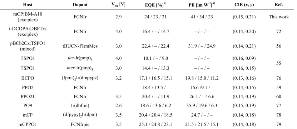
Figure 2.4 (a) JVL characteristics of the devices. (b) The EQEs and PEs of the devices. (c) Normalized EL spectra of devices with various thicknesses of the BM-A10 layer.
30
Figure 2.4a shows the JVL characteristics of the devices with the different thicknesses of the electron injection layer. The device structure was indium tin oxide (ITO) (70 nm)/6 wt% ReO3 doped mCP (30 nm)/mCP (20 nm)/emitting layer (EML, 30 nm)/BM-A10 (20 nm)/12 wt% Rb2CO3 doped BM-A10 (10, 20, 30, 40 nm)/Al (100 nm). The turn-on voltage was 2.9 V.
Efficient hole and electron injection was achieved from the electrodes by p and ndoping, respectively, and the simple device structure with few interfaces resulted in the low turn-on voltage. Figure 2.4b shows the Lambertian corrected EQEs and power efficiencies. The emission patterns of the devices were measured via angle-dependent EL, where the Lambertian correction factors were 0.86, 1.04, 1.06, and 1.14 for ndoped BM-A10 layers that were 10-, 20-, 30-, and 40-nm-thick, respectively. Lambertian correction was implemented according to the method reported elsewhere.32 Figure 2.4c shows normalized EL spectra of the devices at a current density of 10 mA cm-2. As the thickness of the n‒BM-A10 layer increased, the intensity of the vibronic peak of FCNIr increased, which is attributed to the microcavity effect.80 The CIE ycoordinate varied from 0.19 to 0.27 as the thickness of the n‒BM-10 layer increased from 10 to 40 nm. The device with a 10-nm-thick nBM-A10 layer exhibited a maximum EQE of 19% with a power efficiency (PE) of 33 lm W-1. The device with a 20-nm-thick nBM-A10 layer exhibited a maximum EQE of 24% and maximum PE of 41 lm W-1 with a CIE ycoordinate of 0.21.
31
The exciplex host used device showed ten times extended operational lifetime (operational half lifetime LT50 of about 1 hr at 400 cd m−2) compared to other single host devices (a few minutes at the same condition) as shown in Figure 2.3c. The materials are not thermally stable very much with the glass transition temperatures (Tg) of 55.4 and 102 °C for mCP and BM-A10, respectively.74,81 Therefore, the Tg of the mixed film is expected to be lower than 100 °C. Even with the low thermal stability, the device lifetime extended more than ten times, demonstrating the potential of exciplex system for high efficiency and long lifetime OLEDs. Even though the lifetime is too short to be practical in this system, it can be much longer if more stable donor and acceptor materials for blue exciplex are developed.
The experimentally obtained efficiencies are compared with the theoretically calculated maximum achievable efficiencies under the assumption of no electrical losses in Figure 2.3d. The experimentally measured EQEs are approximately 4% smaller than the simulated data. The reason why this device shows lower efficiency than the theoretically achievable maximum efficiencies in contrast to our previous devices based on exciplex hosts is not clear yet and is under investigation. We speculate that the lower efficiencies may originate from the non-confined exciplex T1 or charge imbalance. Even though the energy of the host T1 exciplex can be transferred to the host T1 and finally to dopant molecules, the energy transfer processes are in competition with the non-radiative decay of the host T1 excitons, which can reduce the efficiency
32
from the theoretically achievable ones.66 Carrier mobility should be investigated for the charge balance factor. The hole-only and electron-only devices were fabricated and the structure of hole-only device was indium tin oxide (ITO) (150 nm)/ReO3 (1 nm)/mCP or mCP:BM-A10 (100 nm)/ReO3 (1 nm)/Al (100 nm) and that of electron-only device was ITO (150 nm)/BM-A10 or mCP:BM-A10 (100 nm)/Rb2CO3 (1 nm)/Al (100 nm). To provide Ohmic contact, rhenium oxide (ReO3) and rubidium carbonate (Rb2CO3) were used as a hole and electron injection layer, respectively.12 The J−V characteristics were presented in Figure 2.5a and the space charge limited current (SCLC) regime was analyzed according to the Mott−Gurney theory which is expressed as:
2
SCLC 0 3
9
8 r
J V
L
(2.1)
where J is the current density, ε0 is the vacuum permittivity, εr is the dielectric constant, μ is the carrier mobility, V is the applied voltage, and L is the film thickness.82 At the low electric field region, J−V characteristics show Ohmic current. As the electric field increases, J−V characteristics show SCLC in the region of 150−700 kV cm−1. The extracted mobilities from equation 2.1 are presented in Figure 2.5b. The mobility values are fitted by the Poole−Frenkel model, which is expressed by
0exp(0.89 F)
(2.2)
33
where μ0 is the zero field carrier mobility, β is the Poole−Frenkel coefficient, and F is the electric field.83 Almost 2 orders of magnitude difference between electron and hole mobilities in the EML can lead to the charge imbalance or at least shifted exciton profile toward the ETL inducing exciton loss.84
34
Figure 2.5 (a) Current density−voltage (J−V) characteristics of the hole and the electron only devices. (Open symbols: measured data, solid lines: fitted by space charge limited current (SCLC) model) (b) The hole mobilities of mCP and mCP:BM-A10:FCNIr mixed films, as well as the electron mobilities of BM-A10 and mCP:BM-A10:FCNIr mixed films. (Open symbols: Extracted from the J−V characteristics. Solid lines: Fitted by Poole-Frenkel model.)
35 2.4 Conclusion
In summary, we have developed an exciplex-forming mixed host for deep-blue PhOLEDs. The exciplex host was composed of mCP as the donor and BM-A10 as the acceptor. The emission energy of the exciplex was 3.0 eV, which is sufficiently large for the use of deep-blue dopants. The blue PhOLEDs doped with FCNIr achieved a turn-on voltage of 2.9 eV, a maximum EQE of 24% with CIE coordinates of (0.15, 0.21), and an EQE of 19% with CIE coordinates of (0.15, 0.19). This represents superior color purity compared to blue FIrpic-based devices, which have CIE coordinates of (0.16, 0.33). The exciplex host devices showed much better performances in EQE, PE, driving voltage, and operational lifetime than the single host devices.
36
Highly efficient deep blue OLEDs using TADF emitter with narrow emission spectrum and high horizontal emitting dipole orientation
3.1 Introduction
The development of thermally activated delayed fluorescent (TADF) emitters has greatly improved the efficiency of the fluorescent organic-light emitting diodes (OLEDs).48–50,85 In contrast to the conventional fluorescent emitters, which can only utilize singlet excitons for radiation, TADF emitters can harvest triplet excitons via reverse intersystem crossing (RISC) process and thus enable 100% internal quantum efficiency (IQE). TADF emitters have separated the highest occupied molecular orbital (HOMO) and lowest unoccupied molecular orbital (LUMO) on donor and acceptor units, respectively. The separated HOMO and LUMO minimizes electron exchange energy, resulting in small singlet (S1)-triplet (T1) energy level difference (ΔEST).45 Because of the separated HOMO and LUMO orbitals, TADF emitters show charge transfer (CT) characteristics in radiative emissions. Therefore, the emission energy of TADF emitters can be adjusted by selecting appropriate donors and acceptors. Various donor and acceptor moieties have been utilized to develop blue TADF emitters. Examples include carbazole48,86–88, acridine89–
37
91, phenoxazine49,92, azasiline93–95, and spiro-flourene96 moieties for donor units and cyano97–101, nitrogen heterocycles50,96,102,103, oxygen heterocycles104,105, sulfone49,88,106, methanone28,107, and boron108–111 moieties for acceptor units.
Even after the large development and despite the importance of deep blue emitters with CIE y<0.1 for full-color display and lighting, there have been few reports on highly efficient deep blue emitting TADF emitters due to broad emission spectra of TADF emitters with the full width at half maximum (FWHM) of 70~80 nm. Lee et al. developed a deep blue emitting TADF emitter with large steric hindrance, which exhibited a narrow emission spectrum with the FWHM of 48nm.112 However, the EQE was relatively low (14.0%) compared to blue TADF OLEDs.94–96,108
Recently, novel TADF emitters with narrow FWHM have been reported.
Hatakeyama et al. reported deep blue emitting TADF emitters with narrow FWHM using a nitrogen-bridged boron structure inducing multiple resonance effects.113,114 Kwon et al. and Adachi et al. reported D-A type deep blue emitting TADF emitters adopting an oxygen-bridged boron acceptor unit, which is rigid and has symmetric structure.115,116 The FWHM of the emitters was effectively reduced compared to the emitters using a non-rigid and symmetric acceptor unit, indicating that the nitrogen-bridged or oxygen-bridged boron structures are promising acceptor units for deep blue TADF emitters. Nevertheless, the efficient deep blue TADF OLEDs with EQEs near 30% and the CIE y coordinate under 0.1 have not been reported yet to our best knowledge. The
38
selection of a proper donor unit must be important to realize efficient deep blue TADF emitters because the 1CT and 3CT energy levels are influenced by the donor unit as well as the acceptor unit in the emitters.
In this paper, we report two new TADF emitters for efficient deep blue OLEDs by adopting rigid spiro-type donors and oxygen bridged boron acceptors to demonstrate an unprecedented highly efficient deep blue TADF OLED exhibiting EQE of 28.2% with CIE coordinates of (0.142, 0.090). The high color purity with narrow emission and high efficiency is discussed based on the energies level of the donor units, rigidity, and orientation of emitters.
The high RISC rate of emitters was discussed based on TD-DFT calculation and experimentally measured energy levels.
39 3.2 Experimental
Materials preparation. The highly efficient TADF emitters (TDBA- SAF and DBA-SAB) were designed and synthesized in the Department of Chemistry and Research Institute of Natural Science of Gyeongsang National University supervised by professor Yun-Hi Kim.
Fabrication and PL measurement of organic thin film. Organic thin film was deposited by thermal evaporation on cleaned fused silica substrate in vacuum chamber of which the base pressure was under 5 ×10⁻⁷ Torr. PL spectra measured using continuous He-Cd laser (325 nm, Kimmon Koha Laser Systems) and Maya200 Pro (Ocean Optics Inc.) detector at room temperature.
Measurement of transient PL. Transient PL was measured using an N2
laser (337 nm, Usho Optical Systems Co.) as an excitation source and a streak camera (Hamamatsu, C10627) as a detector.
Fabrication of OLEDs. ITO substrates were cleaned by acetone and boiling isopropyl alcohol. After drying in 80℃ oven, organic layers were thermally evaporated in vacuum chamber of which the base pressure was under 5×10⁻⁷ Torr. After the end of evaporation, all devices were encapsulated in globe box.
40
Measurement of OLEDs. J–V character was measured using Keithley 2400 source meter and EL spectra and intensities were measured using PR650 (Photo Research) in normal direction.
41 3.3 Result and discussion
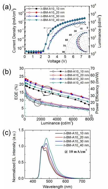
The spiroacridine fluorene –based donor was designed to lower the HOMO energy level due to sp2-hybridized spirofluorene. The spiro-type spiro- biacridine (SAB) and spiro-acridine fluorine (SAF) are expected to have deeper HOMO levels than dimethyl acridine (DMAC) structure with sp3 hybridized CH3 groups due to higher electron-withdrawing property originating from the stronger s character. Kwon et al. reported deep blue emitting TADF emitter consisting of tert-butyl dioxa boranaphtho anthracene (TDBA) and DMAC TDBA-Ac which exhibits blue emission of 458 nm in toluene.115 Therefore, the combination of TDBA and SAB or SAF will give deeper blue emission than TDBA-Ac. In addition, the high rigid structure of spiroacridine fluorene can reduce the vibronic transitions to increase the quantum efficiency and to narrow down the emission spectrum. Moreover, the spiro-type donors construct a longer molecular structure, which is advantageous for increasing the horizontal emitting dipole moment ratio (Θ). Based on the consideration, we designed 10- (2,12-di-tert-butyl-5,9-dioxa-13b-boranaphtho[3,2,1-de]anthracen-7-yl)-10H- spiro[acridine-9,9'-fluorene] (TDBA-SAF), a donor (D)-acceptor (A) type emitter, and 10,10'-di(5,9-dioxa-13b-boranaphtho[3,2,1-de]anthracen-7-yl)- 10H,10'H-9,9'-spirobi[acridine] (DBA-SAB), an A-D-A type emitter, respectively (Figure 3.1b).
The design concept is supported by the density functional theory (DFT) and time-dependent DFT (TD-DFT) calculations. Optimization of excited state
42
geometry was performed with Gaussian 09 employing the functional of CAM- B3LYP and M06-2X for 1,3CT and 3LE state, respectively. Natural transition orbitals (NTOs) were performed using optimized excited geometry with Schrodinger’s Materials Suite Jaguar, employing ωB97X-D (ω=0.1) for 1,3CT transition and M06-2X for 3LE transition. For performing all geometry optimization and single-point energy calculations, the 6-31G (d,p) basis set was employed. Calculated NTOs corresponding to transition from excited state to ground state are depicted in Figure 3.1. The highest occupied natural transition orbital (HONTO) is mainly located at the spiro-acridine fluorene or spiro- biacridine donor unit and the lowest unoccupied natural transition orbital (LUNTO) is mainly located at the boron acceptor unit as expected. The orbital overlap between HONTO and LUNTO is very small and thus emitters would have CT-type transition with small ΔEST. In addition, the calculated NTOs corresponding to 3LE transition turn to be located at the boron acceptor unit.
The calculated energy levels of the 1CT, 3CT and 3LE states are shown in Figure 3.1. The simulations forecast small ΔEST of 0.012 eV, as expected.
Furthermore, the energy differences between 3LE and 1CT, and 3LE and 3CT are small with 0.093 eV and 0.105 eV for TDBA-SAF and 0.257 eV and 0.269 eV for DBA-SAB, respectively, anticipating fast RISC process in the emitters.
43
Figure 3.1 (a) Calculated LUMO level of acceptor units and HOMO levels of donor units. (Gaussian 09, B3LYP/6-31G(d)) (b) Calculated natural transition orbitals (NTOs) of TDBA-SAF and DBA-SAB for 1,3CT and 3LE states. NTO calculations were performed using optimized geometry of each excited states. (1,3CT optimization: Gaussian 09, 6-31G (d,p)/CAM-B3LYP, 3LE optimization: Gaussian 09, 6-31G (d,p)/M06- 2X, 1,3CT single point energy: Jaguar, 6-31G(d,p)/ωB97X-D (ω=0.1), 3LE single point energy: Jaguar, 6-31G (d,p)/M06-2X)
44
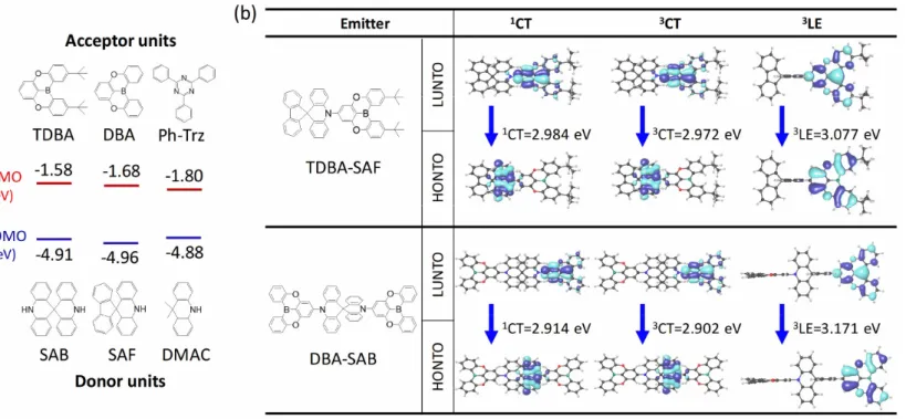
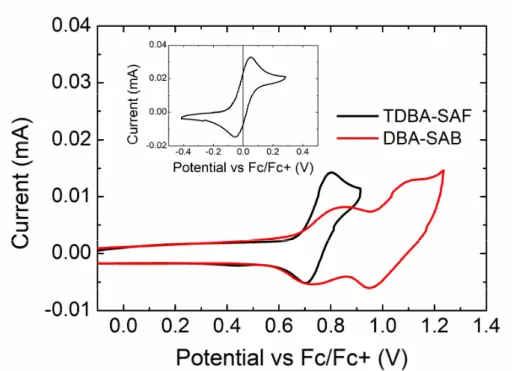
The photophysical properties measured in solution state are shown in Figure 3.2a. The absorption peaks are located at the wavelengths of 381 nm and 375nm and the emission peaks at 450 nm and 460 nm for TDBA-SAF and for DBA-SAB in toluene, respectively. The Stokes shift is larger in DBA-SAB, which is attributed. TDBA-SAF exhibits smaller Stokes’ shift than DBA-SAB because of the restriction of the Frank-Condon factor of the D-A structure than A-D-A structure.108 The small Stokes’ shift is beneficial for the realization of deep blue emission. One can note that the TDBA-SAF emits deeper blue spectrum than the previously reported TDBA-Ac because of the weaker electron donating property of spiro-fluorene substituted acridine than that of dimethyl substituted acridine, as discussed above (Figure 3.3).95,96,115 The bathochromic shift of the PL spectrum with increasing solvent polarity in Figure 3.2 indicates the CT character of the emission of the molecules. The HOMO level was determined by cyclic voltammetry measurements (Figure 3.4) and the LUMO level was determined by adding the optical bandgap of materials to the HOMO level. The HOMO/LUMO level of TDBA-SAF and DBA-SAB was -5.5/-2.4 and -5.6/-2.5 eV, respectively.
45
Figure 3.2 (a) The absorbance and photoluminescence (PL) spectra of TDBA- SAF and DBA-SAB in solution state. (b) Angle dependent PL (ADPL) intensity of p-polarized light from emitter doped DPEPO films. (c) Transient PL decay curves of emitter doped DPEPO films (inset: enlarged prompt decay curves).
46
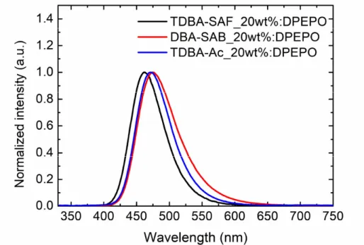
Figure 3.3 The photoluminescence (PL) spectra of TDBA-SAF, DBA-SAB and TDBA-Ac in DPEPO host.
47
Figure 3.4 Cyclic voltammogram scans of solution, with methylene chloride, 0.1 M tetrabutylammonium hexafluorophosphate (TBAPF6) and 1mM TADF emitter. TBAPF6 was used as the supporting electrolyte.
48
The photoluminescence quantum yield (PLQY), EDO and transient decay curve measurements were conducted using the doped films in high T1
host material, diphenyl-4-triphenylsilylphenyl-phosphine oxide (DPEPO).
Both emitters have high PLQYs and horizontal EDO ratios (Θs, defined as the average ratio of the horizontal component of emitting dipole moment to the total emitting dipole moment) of 90 and 81% for TDBA-SAF and 87% and 89% for DBA-SAB, respectively, measured from the 20wt% doped films, respectively (Θ: Figure 3.2b). In addition, both emitters have high Θ values above 80%, which are the dramatically enhanced values compared to that of TDBA-Ac. Especially, DBA-SAB showed much higher Θ than TDBA-SAF due to the longer molecular structure with the direction of CT transition, as discussed before. The transient PL decay curves of emitters (Figure 3.2c), the rate constants of the both emitters were analyzed according to the methods described in reference.49 The calculated rate constants are summarized in Table 3.1. Both TDBA-SAF and DBA-SAB exhibited efficient RISC process with the RISC rates of 2.1×10⁶ s-1 and 1.9×10⁶ s-1, respectively. These RISC rates are similar to that of recently reported TADF emitters using oxygen-bridged boron acceptor, but larger than previously reported blue TADF emitters.92,100,115,116
49
Table 3.1 Photophysical properties and rate constants of TDBA-SAF and DBA-SAB.
PLQY (%)
Θ (%)
ΦPF (%)
ΦTADF (%)
τp (ns)
τd (μs)
kr (x107)
knr (x106)
kISC (x107)
kRISC
(x106)
knrT (x105)
ΦRISC (%)
ΔEST
(eV)
TDBA-SAF 90 81 32 58 30.6 1.34 1.0 1.2 2.1 2.1 0.7 96.6 0.11
DBA-SAB 87 89 47 40 45.1 0.96 1.0 1.6 1.0 1.9 1.4 93.4 0.07
50
In order to further understand the high RISC rates of the emitters, time- resolved PL spectra was taken and the energy level of 1,3CT state was obtained from the onset of the emission spectra (Figure 3.5). At room temperature, the spectral shifts from prompt (~5ns) to delayed emissions (0.5~1.5μs) was 12 nm, which attributed to the narrow conformational distribution or suppressed structural relaxation of TADF emitters.94 The singlet-triplet level energy difference (ΔEST) of the emitters was acquired from the onset of fluorescence and phosphorescence spectra measure at 100K. Both emitters exhibited featureless phosphorescence emission spectra along with the fluorescence emission, ensuring that triplet emission has also the CT character. The measured energies of the 1CT state, 3CT state and the resulting ΔEST are 2.99 eV, 2.88 eV, and 0.11 eV for TDBA-SAF and 2.94 eV, 2.85eV, and 0.09 eV for DBA-SAB, respectively. The experimental values matched well with the calculated values, suggesting that the TD-DFT was conducted with appropriate basis sets and functionals. Despite the larger ΔEST, TDBA-SAF exhibited larger RISC rate constant than DBA-SAB. As Monkman et al. have analyzed, 3LE state can participate in RISC process between 1CT and 3CT states and effe