저작자표시-비영리-변경금지 2.0 대한민국 이용자는 아래의 조건을 따르는 경우에 한하여 자유롭게
l 이 저작물을 복제, 배포, 전송, 전시, 공연 및 방송할 수 있습니다. 다음과 같은 조건을 따라야 합니다:
l 귀하는, 이 저작물의 재이용이나 배포의 경우, 이 저작물에 적용된 이용허락조건 을 명확하게 나타내어야 합니다.
l 저작권자로부터 별도의 허가를 받으면 이러한 조건들은 적용되지 않습니다.
저작권법에 따른 이용자의 권리는 위의 내용에 의하여 영향을 받지 않습니다. 이것은 이용허락규약(Legal Code)을 이해하기 쉽게 요약한 것입니다.
Disclaimer
저작자표시. 귀하는 원저작자를 표시하여야 합니다.
비영리. 귀하는 이 저작물을 영리 목적으로 이용할 수 없습니다.
변경금지. 귀하는 이 저작물을 개작, 변형 또는 가공할 수 없습니다.
이학박사학위논문
The p-Type Conductivity of Stannate Perovskite System
페로브스카이트 주석 산화물의 p형 전도성에 관한 연구
2016년 8월
서울대학교 대학원 물리천문학부
권 혁 우
Doctoral Thesis
The p-Type Conductivity of Stannate Perovskite System
Hyukwoo Kwon
Supervised by
Professor Kookrin Char
A dissertation
Submitted to the Faculty of Seoul National University
in Partial Fulfillment of
the Requirements for the Degree of Doctor of Philosophy
August 2016
Department of Physics and Astronomy Graduate School
Seoul National University
DMS 200920395
권혁우 Hyukwoo Kwon, The p-type conductivity of
Stannate Perovskite System,
페로브스카이트 주석
산화물의 p형 전도성에 관한 연구, Department of
Physics and Astronomy, 2016, 90P, Advisor: Prof. Kookrin Char, Text in EnglishAbstract
Thin films of the transparent oxide semiconductor with a p-type conduction are fabricated by the impurity doping method in the stannate Perovskite system.
Ba1-xNaxSnO3 (x = 0.04 ~ 0.1) thin films were grown by the pulsed laser deposition method and their physical properties were measured. All of films are epitaxially grown with a good crystallinity. Images of the transmission electron microscopy reveal that Na impurity atoms do not severely distort the crystal structure of the host material. Microscopy images of surfaces of films confirm that there is no Na segregation and surfaces of films are smooth enough. Its p-type conduction is indirectly confirmed by the almost ideal characteristic curves of the BNSO-BLSO pn junction. Furthermore, its p-type conductivity is directly verified by the high temperature Hall measurement data, namely the positive Hall coefficients. The 4 % doped BNSO film shows the high p-type mobility of 77 cm2/V∙s with a carrier concentration about 6.9 × 1014 cm-3 around 200 C. Despite the existence of threading dislocations in the film, revealed by the TEM image, there is no dislocation scattering effect, similar to the cases of the p-type Ge and GaN.
Temperature dependences of the hole concentration indicate that hole carriers are largely trapped in localized states at the low temperature due to disorder of the system. Optical measurement confirms the disordered nature by showing the Drude peak shift in the optical conductivity and the Urbach tail state in the optical absorption and reveals that disorder originates from the deep level character of the Na doping. The observed high hole mobility seems closely related to the A-site doping in the Perovskite system.
SrSn1-xRuxO3 films (0.1 ≤ x ≤ 0.3) were grown by the pulsed laser deposition method. X-ray diffraction measurement exhibits that all of the films maintain a single phase over the doping range and lattice constants of the system monotonously decrease as the Ru doping increases. Hall measurement data indicates that the conduction of this system is mediated by hole carriers. Transport measurement shows that this system undergoes the metal-insulator transition depending on the Ru doping rate and their resistivities dramatically decrease as the Ru doping increase. Furthermore, its corresponding mobility values vary from 0.1~20 cm2/V∙s, depending on the Ru doping rate. Optical measurement suggests that there are mid-gap states, which are varying depending on the Ru doping rate.
Magnetic measurement data confirms that mid-gap states with a Mott-Hubbard gap are mainly composed by the Ru 4d character like as the SrRuO3 and the ferromagnetic ordering is closely related with the relative magnitude of correlations (U) and the bandwidth (W), the metal-insulator transition, which is consistent with
the above mentioned mid-gap model. The p-type conductivity of the SrSn1-xRuxO3
system is closely related to the p-type conduction of SrRuO3 at the room temperature, which is originated from the dispersive p-d hybridized valence band and the flat eg conduction band.
Table of contents
Abstract
Table of contents
Chapter 1. Introduction ... 1
1.1. Transparent Conductive Oxides and Transparent Oxide Semiconductors ... 1
1.2. A Brief Introduction of the BaSnO3 and SrSnO3 ... 4
1.3. Obstacles to the p-type Oxide Semiconductor ... 10
1.4. Strategies for p-type Stannate Perovskite ... 13
Chapter 2. A-Site Doping of BaSnO
3... 16
2.1. Introduction. ... 16
2.2. Experiments. ... 20
2.1. Structure Properties of Ba1-xNaxSnO3 Thin Films. ... 22
2.2. Morphologies of Ba1-xNaxSnO3 Thin Films. ... 31
2.3. Transport Properties of Ba1-xNaxSnO3 Thin Films. ... 33
2.4. Optical Properties of Ba1-xNaxSnO3 Thin Films. ... 42
2.5. Discussions on Ba1-xNaxSnO3 Thin Films. ... 52
2.6. Conclusions on Ba1-xNaxSnO3 Thin Films. ... 55
Chapter 3. B-Site Doping of SrSnO
3... 56
3.1. Introduction ... 56
3.2. Experiments ... 59
3.2. Structure Properties of SrSn1-xRuxO3 Thin Films. ... 61
3.3. Transport Properties of SrSn1-xRuxO3 Thin Films ... 68
3.4. Optical Properties of SrSn1-xRuxO3 Thin Films. ... 71
3.5. Magnetic Properties of SrSn1-xRuxO3 Thin Films. ... 75
3.6. Conclusions on SrSn1-xRuxO3 Thin Films ... 79
Chapter 4. Conclusions ... 80
References ... 82
Summary in Korean ... 88
Publication List ... 90
1
Introduction 1
1.1. Transparent Conductive Oxides and Transparent Oxide Semiconductor
In the naïve understanding of the condensed matter physics, the high optical transparency to the visible light and the high electric conductivity are rather contradictory concepts. The optical transparency to the visible light means that the material has a wide band gap with a larger than ~ 3 eV, so it shows the insulating phase, not conductive, at the room temperature in general. On the other hand, a good electrical conductivity means that there are free carriers and there is no gap near the Fermi level. Because of characteristic of the wide band gap, most of possible dopants can be deep level impurities with a large activation energy and they cannot induce the conductivity of the host material. Some dopants of certain host materials, however, have an appropriate dopant level, which donates conduction electrons to the host material and leads to the conductivity of the host material system. Because of the compatibility of rather contradictory properties, optical transparency and electric conductivity, there has been a lot of research in the area of the academy and the industry as called “transparent conductive oxide (TCO)”.
2
The fluorine doped tin oxide, which reflects light below its plasma frequency due to its metallicity, is applied as the energy-efficient windows in tradition. In addition, the market of the flat panel display, the smart device and the solar cell device has grown explosively in recent years and will be rapidly increasing over the next few years. In these applications, the TCO material is used as the top electrode of the light emitting devices (display field) and the light absorbing devices (solar cell field). In brief, most important parameters in these fields are optical transparency, which is closely related to the optical efficiency, and the electrical conductivity, of course. As the size of the display and the speed of writing are increasing, it will be required to low resistivity with a maintaining or enhancement of the optical transparency. Among some candidates of TCO materials, ZnO, SnO2 and In2O3 are representative TCO materials, which are focused by the many researchers. [1, 2]
Although the fascinating success of TCO applications, this success has a rather restricted range due to following reasons. First, most of the TCO material has n-type conductivity but there is a few report on the p-type TCO. That is, there was no active devices due to the absent of bipolar TCO materials. Furthermore, most of the TCO has been focused on a good electrical conductivity with a large carrier concentration that is not controlled intentionally in the majority of cases, therefore it cannot paradoxically demonstrate the off-state of the semiconductor device due to its large carrier concentration. Because of above-mentioned reasons,
3
there are few reports on the transparent semiconductor devices, especially active semiconductor devices such as the optical device. [3]
A breakthrough is made by the first fabrication of the p-type transparent oxide semiconductor, CuAlO2. [4] This achievement leads to a “new frontier” called as the “transparent oxide semiconductors (TOS)”. [5] In the succession of the success of the CuAlO2, studies on this field, transparent oxide semiconductor, are explosive growing in past years. In addition, these TOS materials are applied to the UV-light emitting device (UV-LED) and the transparent thin film transistor (TFT).
Considering the present wavelength range of the light emitting diode, based on the GaN, which is limited to the visible light, UV LED based on the new TOS will be considered as the next generation semiconductor. Moreover, combined with the flexibility of the material, the market of the flexible transparent electronics, wearable electronics, will be rapidly growing in the near future. [3, 5]
4
1.2. A Brief Introduction of the BaSnO
3and SrSnO
3BaSnO3 (BSO) is one of the promising transparent oxide semiconductor, which recently attracts overwhelming attentions of the many researchers because of its fascinating properties. Although BSO is already known in the 1950s, this material has been mostly used as the gas sensor due to its rather larger band gap, compared with the conventional semiconductor such as Si or GaAs. In spite of a proper band gap size as the TOS, there is few report on this material due to the lack of the appropriate dopant, which induces the electrical conductivity of the host material. In recent, the Professor Kookrin Char’s group suggests and reports that a La doped BSO can be a good TOS. [6] In addition, following studies on this material reveals fascinating properties of the BSO as the TOS. In this chapter, the characteristic of the BSO will be described shortly.
BSO is the cubic Perovskite crystal structure with the lattice constant 4.116 Å
.
[6] While the most of the transparent oxide semiconductor recently studied is based on the binary oxide, the BSO is the ternary oxide with two cations. These two cation sites has a crucial role in the doping strategy, explained later. The Perovskite structure, also called ABO3, is composed of BO2 octahedral and an enclosed AO cubic cage. In the case of the BSO, SnO2 octahedral is surrounded by the BaO cubic cage. The SnO2 octahedral decides most of the physical properties of the material and the BaO cage has a role like as a support fixture in the cubic structure, which is a general property of the Perovskite structure. In the case of the octahedral tilting,5
which is induced by the change of the size of the AO cage, related with the Goldschmidt tolerance factor, the A site cation has a large influence to the physical properties of the material, which is further described later.
As mentioned above, the band gap size of BaSnO3 is ~ 3.1 eV, which corresponds to the wavelength of ~ 400 nm, a range of the violet color. [6] Therefore, the BSO has the optical transparency to the visible light. In addition, the transmittance of the BSO single crystal is almost 0.7, which is large enough to be applied as the transparent oxide semiconductor. [7] According to the former paragraph, this optical transparency is closely related to the physical properties of the SnO2 octahedral, which is also a transparent material with ~ 3.6 eV band gap.
As mentioned earlier, this trend is generally common in the Perovskite system because of their similarity in the band structure, near the valence band and the conduction band, which mostly decides the physical properties of the material. For example, the size of the band gap of the BaHfO3 and SrTiO3 is around 5.1 eV, 3.25 eV and that of the HfO2 and TiO2 is 5.3 ~ 5.7 eV and ~ 3.2 eV.
The most exceptional characteristic of the BSO is its high electron mobility.
The electron mobility of the 4 % La doped BaSnO3 epitaxial thin film is around 90 cm2/V·s with a carrier concentration 4 1020 cm-3 and that of the single crystal BaSnO3 reaches 320 cm2/V·s with a carrier concentration 8 1020cm-3. [6] These values are very high compared with other transparent oxide semiconductor and the GaN considering their rather high carrier concentration. The origin of this high
6
mobility is not fully understood but there are possible reasons for this high value.
[6]
In addition, there is a discrepancy between the mobility of the epitaxial thin film and the single crystal. This discrepancy is closely related to the existence of threading dislocations in the epitaxial thin film, which originates from the large lattice mismatch of the BSO thin film and its substrate SrTiO3. Regarding relations of the mobility and the carrier concentration of the thin film and the single crystal, while transport properties of single crystal are governed by the ionized impurity scattering that appears in the n-1 dependence of the mobility curve, that of the thin films are mainly limited by the charged dislocation scattering, which is shown in the n1/2 dependence of the curve. [6]
In brief, the lattice mismatch of the SrTiO3 (STO) substrate (3.905 Å ) and the BSO films (4.116 Å ) inevitably leads to the “malocclusion” of the atoms in the epitaxial growth. In the excess of the critical thickness of the film, which is decided by the strain form the substrate and the tensile strength of the film, atoms in the film tend to be located in the bulk position. Therefore, there should be misfit dislocations in the interface of the film and the substrate. The misfit dislocations induces two threading dislocations to make a dislocation loop in order that reduces the strain on the interface, spreading the elastic energy to the surface. These threading dislocations have dangling bonds, the lack of electrons in the bonding due to the missing line of ions in the thin film, and these can act as electron traps in the solid
7
to fulfil its unfilled valence in bonds. In the limit of the low carrier concentration, these dislocations are partially filled by electrons, so these play a role as additional ionized, due to deficiency of electrons in the bonding, impurity scattering centers and leads to low mobility in the film. As increasing the carrier concentration by the additional doping, these dislocations are filled with free electrons, namely shielded by electrons, and no longer affect in the transport properties in the end, which are governed by the ionized impurity scattering mechanism beyond a certain point.
After all, because of the absent of the suitable substrate that is lattice matched with the BSO, the mobility of BSO thin films are limited by the dislocation and a finding of proper substrates can be one of the important project in this field. [8]
Another fascinating property of the BSO system is its chemical stability even in the high temperature. Most of the transparent oxide material have a problem of the oxygen stability except a few material. In the previous report of our group, however, BSO has an exceptional chemical stability, which is confirmed by its low diffusion constant and a scant variation of resistances under the change of the gas atmosphere at the high temperature. [6] Its remarkable stability is the motivation of the p-type doping in the BSO.
SrSnO3 (SSO) has many similarities to the BSO, which is only differ from BSO in the A site atom. Mentioned earlier, physical properties of the Perovskite system is mainly determined by the BO2 octahedral, therefore there should be resemblances of two material. SSO has the orthorhombic Perovskite structure with
8
the lattice constant 4.03 Å and its optical band gap is around 4.1 eV larger than that of BSO. [9, 10] Like the BSO, SSO is electrically insulation at the room temperature and shows the diamagnetism, no magnetic ordering, because of its fully filled valence states.
There is a relation about variations of physical properties depending on the change from the Ba ion to the Sr ion in the ASnO3 system. Because of the size of the Sr ion (118 pm) is smaller than the Ba ion (135 pm), the overall volume of the SSO is naturally shrinking. In the progress of the contraction in the volume, the SnO2 octahedral is inevitably contracted and distorted in a certain way. This octahedral distortion leads to the structure transition from the cubic to the orthorhombic structure. [9] It is known that this transition is governed by the Goldschmidt’s tolerance factor, which is defined by the ionic radii of the A, B and oxygens, and in ASnO3 system this factor is decided by the ratio of the amount of the Ba and Sr. [11]
The tilting and shrinking of the SnO2 octahedral means that the bonding length of the Sn-O is decreasing. Thus, orbital overlap between Sn and O ions and bonding strength are increasing as a result. As mentioned earlier the conduction band and the valence band are mainly decided by the Sn 5s orbital and O 2p orbital, the band gap of SSO is larger than that of the BSO. Moreover, an octahedral tilting leads to band folding in k-space, the conduction band minimum is shifted to the gamma point. Therefore, SSO has a direct band gap unlike BSO and this is a very
9
interesting property regarding the future application of SSO as a UV-LED. [12]
10
1.3. Obstacles to the p-type Oxide Semiconductor
Most of transparent conducting oxide material have good n-type transport properties by a suitable doping. Therefore, applications of TCO or TOS material are manly focused on the n-type doping and its transport properties. Thus, there is little report on p-type transparent oxides. There are generally two main obstacles to fabricate the p-type transparent oxide semiconductor.
Most of oxide material, except very large band gap material such as Al2O3
and SiO2 etc., have the problem of the intrinsic oxygen vacancies. The amount of oxygen vacancies differs in case by case. Nevertheless, in the case of most of oxides, oxygen vacancies is a crucial problem in material properties and applications, especially in stability of the material and the device. Oxygen vacancies, absent of oxygen atoms, act as a n-type donor in the oxide material, which are detached in the molecular form, O2 , and leave two electrons in the system. In other words, oxygen ions play a role of a glue with the electron reservoir, each oxygen atom keeps two electrons to form a boning with surroundings. In the majority of cases, the energy level of the oxygen vacancies, the oxygen vacancy band, is shallow enough to contribute the electrical conductivity of the oxide material. Many oxides have the intrinsic n-type conductivity for the former reason. In the p-type doping mechanism, these unexpected donors of oxygen vacancies compete with and compensate intentional p-type acceptors. In many cases, extrinsic acceptors, in the solubility limit, cannot overcome intrinsic donors of vacancies due to its instability,
11
thus p-type TOS is hard to fabricate in general. BSO however, have an advantage in the making p-type oxides because of its exceptional chemical stability that is mentioned in the former chapter.
Another hurdle to fabricate p-type TOS is its low mobility due to the flat valence band of oxides. The valence band of oxides is mainly composed of the O 2p states as mentioned earlier. The oxygen atom has the second largest electronegativity in the nature. This large electronegativity leads that electrons, in the bonding between oxygen atom and the other atom, are located in near the oxygen atoms, namely increasing the ionic character in bonding. It means that oxygen ions maintain its ideal shape of the orbital with the fully filled valence and bands of oxygen ions have the less dispersion like as bands of core electrons.
Furthermore, in the cubic Perovskite structure, the angle of the Sn-O-Sn bonding, which is the conduction channel of the system, is 180°, namely the linear bonding.
In this geometry, a missing p orbital is unpaired with the Sn 5s orbital and remain the “nonbonding” state. This nonbonding state acts like as core electrons by definition and induces to the very flat band that is located in the top of valence band, which is mainly charge in the transport properties of p-type the material. In this reason, most of p-type oxide has the lower mobility that that of n-type oxide material, which has the dispersive cation s orbital in the majority case.
In order to overcome this flat band, there are two main streams, which are mainly manipulating the valence band. Remarking that the position of energy level
12
of some cations are enough close to hybrid the oxygen 2p valence band, some material shows the intrinsic p-type conductivity with the enhanced mobility. The first trial and founding is above mentioned CuAlO2, which is based on hybridization Cu1+ and O2- ions and this hybridization induces an additional dispersions of the valence band maximum. [4] And there are many similar trials. [3, 5] Another method is the mixing with the sulfur and the selenium in order to induce the dispersion of the valence band using its rather shallow energy level and lesser low electronegativity. [3]
Another method, our trial method, is separating the doping region and the conduction channel region, namely atomic scale modulation doping in the Perovskite structure owing to its ternary property. As mentioned earlier, conduction channel and its network is only composed of Sn and O ions and A-site ions, Ba or Sr, are just support fixture of the crystal structure. Therefore, A-site doping is less effects, scatterings, in conduction mechanism like as a modulation doping method.
This method does not induce an additional dispersion on O 2p band but can minimize the scattering of impurities.
13
1.4. Strategies for p-type Stannate Perovskite
As mentioned earlier, we try to fabricate the p-type doped ASnO3 remaking on the exceptional chemical stability of the BSO and SSO. Furthermore, because the ASnO3 Perovskite structure have additional candidates of doping sites with respect to the binary oxide material, the ASnO3 system have advantages in making p-type semiconductor.
To fabricate the p-type semiconductor by the extrinsic doping method, we consider some criteria. First, dopants should be acceptors, capturing an electron, in the host material, of course. The ASnO3 system constitutes of the A2+, Sn4+ and O2-. Therefore, 1+ valence for the A site, the 3+ valence for the Sn site and the 3- valence for the oxygen site are needed to fulfil the criterion for the p-type doping. Moreover, the radius of dopant ions are the other criterion for the p–type doping. If the radius of dopant ions are too large or small in comparison with that of the host material, dopants induce the lattice distortion in the case of a large dopant or locate in the interstitial position, which generally acts as a donor in the host material. Thus, the size of dopant ions are also a crucial criterion for the p–type doping.
It is possible that the nitrogen replaces the oxygen site for the p–type doping and this strategy has been tried a lot in the binary oxide system especially in the ZnO. We also try to the nitrogen doping by growing under the N2 atmosphere, but this trial is not successful to enhance the p–type conduction. Thus, we
14
provisionally conclude that the direct nitrogen doping by the PLD method has a problem to making the p–type BSO and exclude the oxygen site doping.
There are two available sites for the p–type doping, the A site and the Sn site. At first, there is the only candidate, the alkali metal, for the A site doping.
The Li ion is too small in comparison with the Ba ion, thus it will locate in the interstitial site and act as an n-type donor in the host material. It is rather common that the Li ion places in the interstitial site and donates an electron in the system due to its unusual size. And the Rb ion and the Cs ion is rather larger than the Ba ion, it may induce the lattice distortion and the unexpected effect in the system.
Furthermore, there is a technical problem in doping Rb and Cs. The ionic radius of the K ion is very similar with that of the Ba ion, the K is the one of the best candidate for the p-type dopant and the previous research of our group report the p–n junction using the K doped BaSnO3. [13] The Na ion is rather smaller than the Ba ion, but this ion has larger ionization energy compared with the K ion, which means that the impurity energy level of the Na ion is shallower than that of the K ion. Therefore, the Na ion is also a good candidate for the p-type dopant.
The Sn ion has rather large valence, +4, so, there are many candidates for p-type dopants. Our group’s trial on B-site doping is, however, not successful in the case of In, Ga and so on. Therefore, we remark on p-type conductivity of SrRuO3
and we find a paper, which reports p-type semiconducting behavior of SrSn0.5Ru0.5O3 films. [14] But there is no serious study on SrSn1-xRuxO3 system as a
15
p-type semiconductor and its mechanism. Thus, we try to fabricate p-type semiconductor of SSO by the Ru doping.
16
A-Site Doping of BaSnO
32
2.1. Introduction
In the naïve view of the theory of the condensed matter physics, the optical transparency, the wide band gap and the insulating phase, and electrical conductivity is rather contradictory concept. But “the transparent conductive oxides (TCO) successfully chase two hares at once.” Materials in this class have been applied in several ways such as energy efficient windows, solar cells and touch screens. Most of former mentioned TCO material have the n-type conductivity based on ZnO, SnO2 and In2O3. [1, 2] Despite the fascinating success of TCO applications, there are few reports on the active transparent device due to the lack of the p-type transparent semiconductor [3] and demonstration of the off state in device due to emphasis on researches to enhance the conductivity. A breakthrough is made by the first fabrication of the p-type transparent oxide semiconductor, CuAlO2. [4] This achievement leads to a “new frontier” called as the “transparent oxide semiconductor (TOS)”. [5] Following the success of the CuAlO2, studies on this field have been explosively growing in past years such as ZnRh2O4, LaRhO3
and so on. These TOS materials will be applied to the UV light emitting device, the transparent thin film transistor and flexible transparent electronics (wearable electronics). [5] There are, however, some shortcomings. Most of above-mentioned
17
p-type materials have intrinsic, not intended, p-type conductivity. In these materials it is hard to intentionally control the carrier concentration of the sample in general, thus there are some difficulties to apply to a variety of semiconductor devices.
There are small amount of reports on extrinsic p-type oxide semiconductors such as ZnO: Ga, N and SnO2: In, Ga etc., but there are still some controversies on their reliability and its rather complex doping mechanism, the co-doping method.
Furthermore, reported p-type oxides have rather small mobilities compared with that of the p-type GaN. (GaN: ~ 100, CuAlO2: ~ 10, LaRhO3: ~ 0.2, NiO: ~ 0.4 and ZnO: Ga, N: ~ 70 cm2V-1s-1)
Recently, BaSnO3 (BSO) is intensely studied by several groups, including ours, because it is one of the promising candidate for the field of the TCO and the TOS. BSO has the cubic Perovskite structure with a lattice constant 4.116 Å and its size of the band gap is around 3.1 eV, transparent to the visible light. Furthermore, the Ba0.96La0.04SnO3 (BLSO) thin film has the exceptional high electron mobility around 90 cm2V-1s-1 with a carrier concentration 4 1020 cm-3 and that of the single crystal BLSO reaches 320 cm2V-1s-1 with a carrier concentration 8 1019cm-3. These values are very high compared with other transparent oxide semiconductor and even with the GaN considering their rather high carrier concentration. Another fascinating property of the BSO system is its chemical stability even at the high temperature, which is confirmed by its low diffusion constant and a scant variation of resistances under the change of the gas atmosphere at the high temperature. [6]
18
There are some obstacles to make p-type oxide semiconductors, for example compensations by oxygen vacancies and the low mobility due to its flat oxygen 2p valence band. Regarding the fascinating chemical stability of BSO, it is, however, believed that oxygen atoms with a small diffusion constant are almost immobile and located in the suitable position. Therefore, this system is relatively less affected by oxygen vacancies and it is expected that the charge compensation effect by vacancies will be negligible. Moreover, BSO has the perovskite structure, in which the conduction network consist of Sn-O-Sn channel and the A-site cation only acts as a support to maintain the crystal structure and has a little role in the electronic structure of the host material. Therefore, the A-site doping is thought as an atomic scale modulation doping, which donates or subtracts electrons from the metal-oxide octahedral without the altering the electronic properties of the system.
In these respects, BSO is the promising candidate for the bipolar dopable semiconductor.
In this chapter, we will report structure properties and morphologies of Ba1- xNaxSnO3 (BNSO) (x = 0.04 ~ 0.1) thin films. Its p-type conductivity is confirmed by its p-n junction characteristics and the high temperature Hall measurement.
Furthermore, its p-type mobility is rather higher among p-type oxide semiconductors. From DC transport measurement data, we reveal that many carriers are trapped in localized states at the room temperature. Optical measurement data confirms its localized behavior and it originates from the deep
19
level character of Na dopants. And we briefly remark on the high mobility of BNSO films.
20
2.2. Experiments
We grow epitaxial thin films of BNSO by using the pulsed laser deposition technique. Commercial 5 × 5 × 0.5 mm3 SrTiO3 (001) substrates are used in the structural, DC transport measurement and the ellipsometry measurement. 0.7 % Nb doped SrTiO3 (001) substrates are used to obtain scanning electron microscopy (SEM) images and MgO (001) substrates are used in the optical absorption measurement owing to its very high band gap. Two commercial ceramic targets, BaSnO3 and Na2SnO3, are used and the ratio of doing is controlled by the target rotating system. A 100 nm thickness of the BSO is deposited as a buffer layer at the temperature 750 C, under the oxygen pressure of 100 mTorr. Considering the volatile property of Na atoms, 200 nm thickness of BNSO films are deposited at the temperature 650 C, under the same oxygen environment. A KrF excimer laser (λ=
248 nm) with the laser fluence of 1.3 ~ 1.5 J/cm2 is used for all films. For the p+
contact in the van der Pauw measurement, SrRuO3 (SRO) is deposited at four corners of thin films. A p-n junction of BNSO and BLSO is fabricated by four sequential growths at the high temperature using Si shadow masks, which is the same as our previous work. [13] A detailed structure of the junction is shown in the Fig. 9.
Structure properties, θ-2θ scans and ω-rocking curves, of thin films are acquired by using the PANalytical X’Pert Pro diffractometer with Cu Kα x-ray source of 1.54056 Å wavelength. High resolution transmission electron images
21
(TEM), Laue diffraction patterns and EDX results are obtained by the Tecnai F20.
Using the MIRA3 Tescan SEM and the NX-10 of the Park system (AFM), morphologies of the sample are scanned. The high temperature Hall measurement with the van der Pauw method is conducted by using our lab-made probe station with the Keithley 4200 semiconductor characterization system and a rotatable permanent magnet of 0.5 T. A reliability of this system is verified by the cross checking of BLSO 4 % films using the commercial BIO-RAD HL5500PC Hall measurement system. Doping percentages of Na atoms are measured by the electron probe micro analysis (EPMA) method using the JEOL JXA–8900R model.
Optical conductivities are measured by terahertz time-domain transmission spectroscopy (THz-TDS) with a Teraview TPS 3000 pulse spectrometer over a frequency range of 0.1-3 THz (3-20 cm-1 of 0.5-2.5 meV) and by Fourier transform infrared spectroscopic ellipsometry (FTIR-SE) with a Sopra GES5 over a frequency range of 600-5000 cm-1 of 0.075-0.625 eV). Above the measurement methods provided an excellent probe method for determining complex optical constants of thin films without Kramers-Kronig analysis. Measurements of optical transmission in the near-infrared, visible, and ultraviolet regions (wavelengths between 3300 and 175 nm) are carried out with a Varian Cary 5000 spectrophotometer for investigating band gaps and band tails in disordered thin films.
22
2.3. Structure Properties of Ba
1-xNa
xSnO
3Thin Films
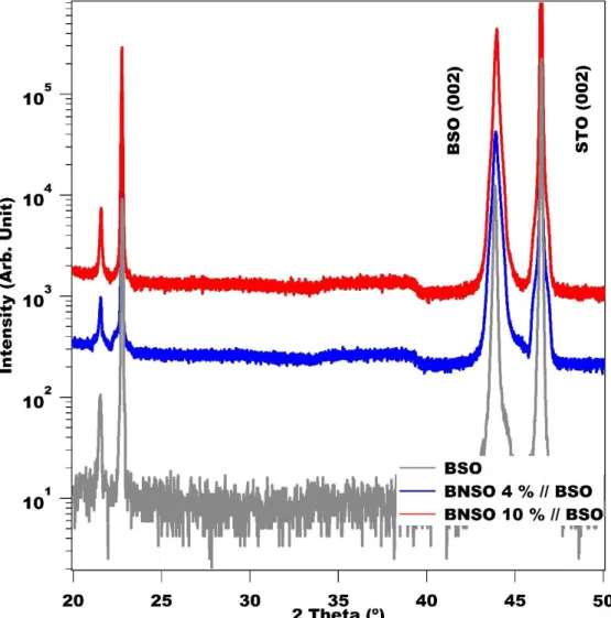
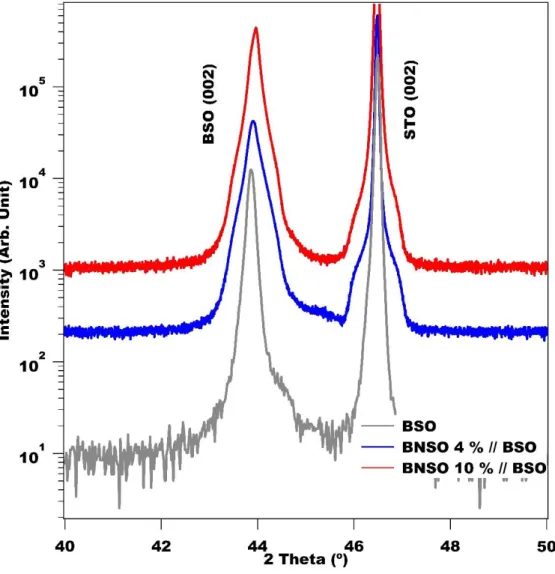
Structural properties of the thin films are surveyed by the X-ray diffraction measurement. Based on the wide scan of θ-2θ scans (Fig. 1), there is no undesired phase except BNSO [0 0 l], which indicates that thin films are grown epitaxially along the c-axis of the substrate and the solubility of the Na atom is larger than our trial doping rate. In addition to the epitaxy, the systematical right shift of the peak position depending on the Na doping is measured that is shown in Fig. 2. Because of the smaller ionic radius of Na ion (Na1+: 102 pm, Ba2+: 135 pm) the lattice constant in the growth direction decreases as the Na doping rate increase. And from this fact, we can legally conjecture Na ions do not locate in interstitial sites and well-mixed in films as expected. The ω-rocking curve (Fig. 3) shows that although the crystallinity of the film, the alignment of the Bragg plane, is rather lowered by the Na doping, (FWHM: 0.083°) the crystallinity of doped films is good enough for following measurements.
23
Figure 1. θ-2θ Scans Results of BNSO Thin Films (Wide Scans)
24
Figure 2. θ-2θ Scans Results of BNSO Thin Films (Magnified)
25
Figure 3. ω-Rocking Curve of BNSO Thin Film
26
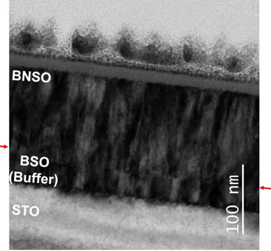
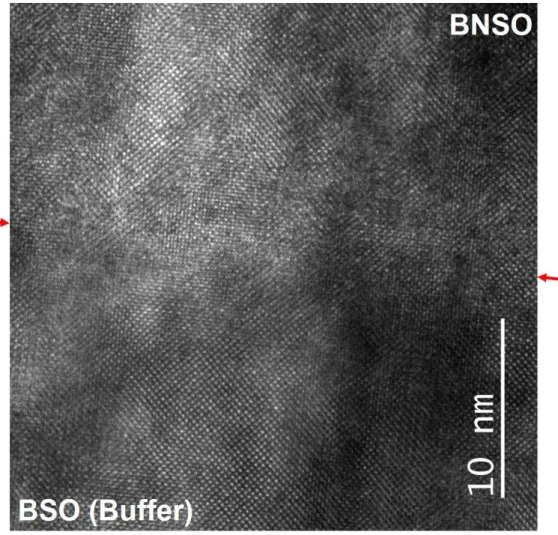
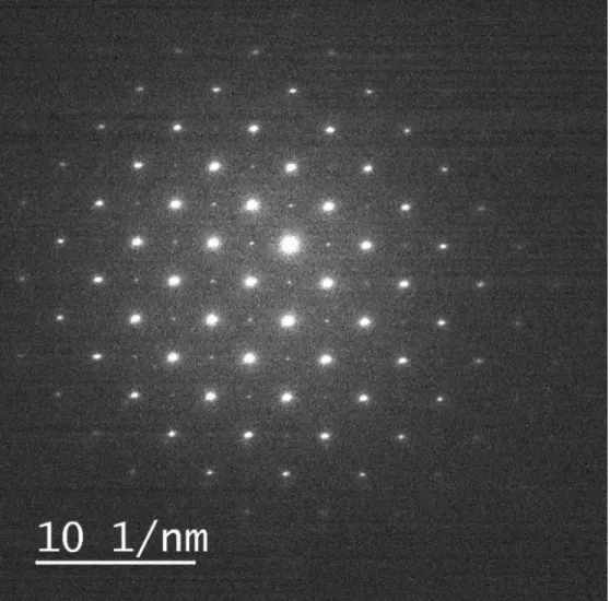
TEM images of the BNSO 5 % film are shown in the Fig. 4. The thickness of the BNSO film is around 120 nm and the below the film 20 nm thick BSO is deposited as the buffer layer on the STO substrate. Because of the large mismatch between BSO and STO (BSO: 4.116 Å STO: 3.905 Å ) there are a lot of threading dislocations in the film, which are shown as vertical dark lines in the figure. In the high resolution image, there is no remarkable difference in the array of ions between BSO buffer layer and BNSO in our inspection. Furthermore, the Laue diffraction pattern of the BSO buffer layer and the region of BNSO also confirms that the BNSO region maintains the cubic phase and the lattice constant, reciprocal of the distance in the Laue image, is almost the same as that of the XRD measurement.
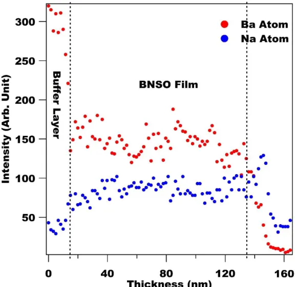
Based on this result, we can conclude that Na doping does not affect severe damages in the crystal structure of BSO and it can act as a dopant as a normal way. The spatial distribution of Na dopants in the film is examined by the energy dispersive X-ray spectroscopy (EDX). We measure the relative amount of Ba ions and Na ions along the vertical direction of the film. In the buffer layer there is a negligible signal of the Na ion, which means no diffusion of dopants to the buffer layer. The ratio of Ba and Na ions are almost constant in the region of BNSO layer, which confirms that Na ions are equally distributed in the film.
27
Figure 4. TEM Images of BNSO Thin Films (Low Resolution)
28
Figure 5. TEM Images of BNSO Thin Films (High Resolution)
29
Figure 6. Laue Diffraction Pattern of BNSO Films
30
Figure 7. EDX Results of BNSO Thin Films
31
2.4. Morphologies of Ba
1-xNa
xSnO
3Thin Films
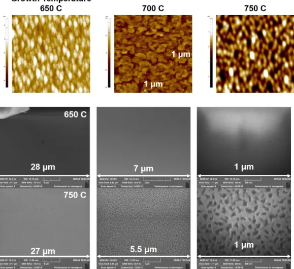
Morphologies of BNSO films are studied by the scanning electron microscopy (SEM) and the atomic force microscopy (AFM), shown in Fig. 8. The left one is the low magnified (× 10000) SEM image. Scanned size of the SEM image is large enough (28 μm × 28 μm) to judge the segregation of dopants or other mesoscopic flaws of the surface. In the SEM image we cannot find any segregations or flaws on the surface except a macroscopic dust. A small area (1 μm
× 1 μm) of the film was surveyed by the AFM. The size of grains is small and very uniform. And the roughness of surface is smooth enough (1.781 nm).
32
Figure 8. Morphologies of BNSO Film depending on the Temperature
33
2.5. Transport Properties of Ba
1-xNa
xSnO
3Thin Films
We try to confirm its p-type conductivity by the fabrication and the measuring I-V characteristic of the p-n junction (BNSO-BLSO). The detailed structure of the junction is shown in the Fig. 9. The p-type material is the BNSO 5 % and the n-type material is the BLSO 0.5 %. Considering the large difference in carrier concentrations of two materials, BNSO are deposited as thick as possible.
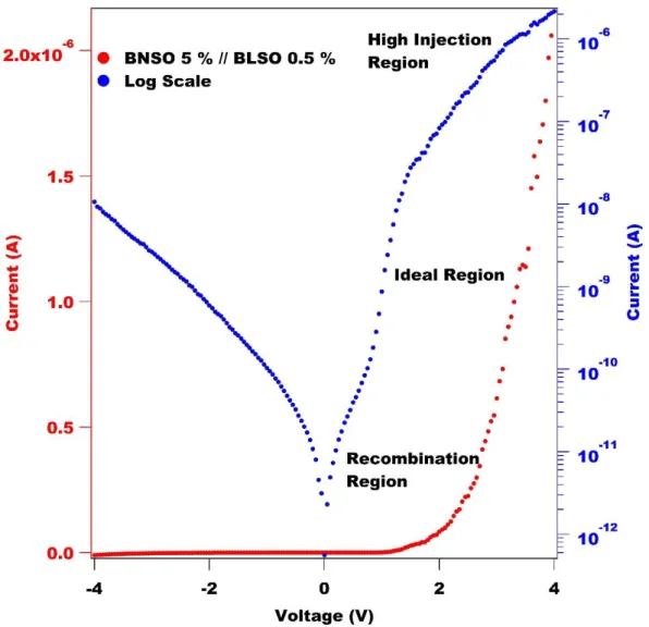
And SrRuO3 and BLSO 4 % are deposited as a p+ and n+ contact to reduce contact resistances. The measured I-V characteristic of the junction is shown in Fig. 10.
The red one is plotted in the linear scale and the blue one is in the log scale. In the linear scale, it almost shows the ideal rectifying curve in the measured range. In the log scale, there are three distinguishable regions in the positive bias. The first region is called as the recombination region, in which the current is limited by the recombination of holes and electrons in the depletion region. The second region is called as the ideal region that shows the ideal rectifying behavior. The last region is the high injection region, in which the current is limited by the series resistance of the overall junction circuit. [15] This behavior is shown in many ideal p-n junctions such as the commercial LED or well-made p-n junctions with a good interface of p and n material. Judging from these data, BNSO has a p-type conductivity with a good interface like as Ba1-xKxSnO3.20
34
Figure 9. A Schematic of the p-n Junction
35
Figure 10. I-V Characteristics of the p-n Junction
36
We acquire transport data by the high temperature Hall measurement due to its high resistance of films (R ≫100 GΩ) at the room temperature. Results are shown in Fig. 11. First of all, all of Hall coefficients, inversely proportion to the carrier concentration, have positive values, which directly verify the p-type conductivity of films. Resistivities of two films rapidly decreases from 118 and 63.4 Ω·cm to 0.21 and 0.355 Ω·cm in each case of 4 % and 10 % BNSO as the temperature increases, which is a typical tendency of the wide band gap semiconductor. In spite of the difference in doping rate (4 and 10 %), the resistivities of two films show very small difference in the measured range. On the contrary, the carrier concentration explosively increases from ~ 1014 cm-3 to ~ 1018 cm-3 as the temperature is elevated. Ratios of carrier concentrations of two films at the same temperature (350 ~ 450 C) are 2.4 ~ 2.5 and considering the doping rate these values are reasonable. Mobilities of two films have the same tendency with the resistivity curve but the differences of two films are remarkable. Although the BNSO 10 % film have more hole carriers, resistivities of two samples are very similar owing to the high mobility of the BNSO 4 %. And the mobility at the temperature 216 C reaches 77 cm2/V·s with a carrier concentration 6.9 × 1014 cm-
3 and this is quite a high value among p-type oxide semiconductors.
37
Figure 11. High Temperature Hall Measurement Results of BNSO Thin Films
38
Mobility vs. carrier concentration of two films is plotted in the Fig. 12. The mobilities and the carrier concentrations are obtained at different temperatures, written in black numbers. Despite the existence of threading dislocations in films that is confirmed in the TEM image, there appears no effect of the threading dislocations on the transport property, completely different from the n-type BLSO.
Although dangling bonds in threading dislocations act as electron traps, the energy level of dislocations is placed near the conduction band, therefore there is almost no effect on the transport property in the p-type material. [16, 17] Considering that the transport property of n-type BSO is limited by the dislocation scattering [6], this fact can be very useful in future applications such as the 2-dimensional hole gas.
39
Figure 12. A Mobility vs. Carrier Concentration Graph of BNSO Thin Films
40
Temperature dependence of carrier concentrations of two films is shown in the Fig. 13. Solid lines are experimental data and dashed lines are calculated from the conventional semiconductor picture. Overall impurity atoms density (n0) is obtained from EPMA results. We cannot fit our experimental data by simple Arrhenius plot. That is, BNSO system cannot be explained by a simple conventional semiconductor picture. It seems that hole carrier concentrations approach values of the conventional semiconductor picture at the high temperature with an activation energy is 0.4 eV, similar with the activation of BKSO in our previous work. [13]
However, the difference between this simple model and the values of experiments is increasing rapidly at the low temperature. Based on this data, we can infer that hole carriers are largely bounded in a certain trap, localized states. This localized behavior is common in the disordered system. [18, 19]
41
Figure 13. A Carrier Concentration vs. Temperature of BNSO Thin Films
42
2.6. Optical Properties of Ba
1-xNa
xSnO
3Thin Films
We measure optical properties to complement evidences and behaviors of the disorder of the system. First we measure the optical conductivity of BNSO thin films by the terahertz transmission and the ellipsometry method shown in Fig. 14, 15 and 16. It seems that all of optical conductivity of samples converge to zero values at the zero frequency (DC limit), which is consistent with our DC measurement. Although conductivities above 15 cm-1 could not be measured due to opaqueness of the STO substrate, the peak position of optical conductivities are located at the finite wavenumber and optical conductivities are increasing as the Na doping raises, which means that localized carriers are increasing depending on the doping rate. Considering the high doping rate of Na and comparing with the case of a shallow level doped traditional semiconductor, impurity bands should be completely delocalized and the optical conductivity data should be the Drude type.
[20] But in the case of BNSO films, peak shapes are shifted to the high wavenumber due to the disorder of the system, which indicates that carriers in the continuum level, near the valence band maximum, are localized. [21-25] Fig. 16 shows optical conductivity over a frequency range of 600-5000 cm-1. There are impurity states around 150 meV and this peaks are shift to the lower energy as the doping rate increases because of the broadening of the impurity band. Very large peaks at the ~ 625 cm-1 are attributed to transverse optical phonon mode of the BSO. [26, 27] The second peak of the BNSO 10 % films, located at ~ 1500 cm-1, is due to the rather
43
thin BSO buffer layer, which is confirmed by the same measurement of 100 nm BNSO with a 20 nm BSO buffer layer films. Based on this data, Na ions are well doped in the BNSO system and they make the impurity band.
44
Figure 14. Optical Conductivities of BNSO Films
45
Figure 15. Optical Conductivities of BNSO Films (Terahertz Region)
46
Figure 16.Optical Conductivities of BNSO Films (Ellipsometry)
47
We try to explore detailed features and the origin of the disorder by the optical absorption measurement. Because the band gap of the STO substrate is lower than that of BSO, we use commercial MgO substrates. Results are shown in the Fig. 17. Because the BSO has the indirect band gap, we plot the square root of absorption coefficient vs. electron energy. The band gap of the BSO is 3.1 eV, which is the same as the single crystalline of BSO. [7] Band gaps of Na doped films are quite shrinking and the degree of shrinking is somewhat dependent to Na doping concentration. This narrowing of the band gap is common in the disordered system and originates from band tail states. [21, 27-31] One way of measuring these tail states is the Urbach tail in the log plot of the absorption coefficient vs. energy in Fig. 18.
[30] The slope of the absorption coefficient in the linear region is closely related to the disorder of the system. Although temperature affects the slope of the linear fitting due to lattice vibrations, all our measurements were conducted at the room temperature, so we can extract the relative disorder of samples from the difference of Urbach energies. [28] The slope of linear fitting is converted to the Urbach energy, the reciprocal of the slope, drawn in Fig. 19. BSO shows quite a small value but it rapidly increases with a small doping of Na. The Urbach energy values slightly increase as the doping rate rises. From this result, we can legitimately conjecture that disorder mainly resulted from the Na doping and the compositional disorder due to the high doping rate is relatively small effect in the disorder. This statement can be supported by our previous study on n-type BSO. In the case of the n-type
48
BSO films with the similar doping rate of the BNSO films, there are no disorder effects such as carrier trappings or the localization modified Dude fitting thanks to the shallow level character of La and Sb. [32] From this comparison, we can conclude that the deep level character of Na doping is the main reason of the disorder of the BNSO system.
49
Figure 17. Optical Absorptions of BNSO Thin Films (α1/2 vs. E)
50
Figure 18. Optical Absorptions of BNSO Thin Films (Log α vs. E)
51
Figure 19. Urbach Energy vs. Na Doping Percentage
52
2.7. Discussions on Ba
1-xNa
xSnO
3Thin Films
From the DC measurement and the optical measurement data, we reveal that BNSO thin films have the disorder. There are some possible origins of the disorder such as a completely broken translational symmetry in amorphous system or compositional disorder in alloy system and heavily doped system or a potential depth and width variation in deep level doping. Regarding the structural data, BNSO thin film system maintains translational symmetry so we can exclude the spatial disorder like as the amorphous state. Although our trial doping rate is rather high compared to the conventional semiconductor system, considering the optical absorption data and the case of the similar doping rate of BLSO system, the compositional disorder is not a main reason of the disorder in BNSO films.
Therefore, we can legally conjecture that the variation of the potential depth due to deep level dopants is the main reason of the disorder in BNSO thin films.
Considering the high temperature carrier concentration and estimated the activation energy (400 meV) and our previous work, acceptor level of Na is considered as quite a deep level. Regarding the deep energy level of the Na, which means that the difference of depth of the periodic potential of Ba and Na is large, the system is largely perturbed by the disorder of the potential depth, that is, Anderson model. [21]
Due to its large discrepancy of the potential depth, localized states are overwhelming extended states, so the mobility edge is located far from the valence band maximum. These tail states and localization behavior can be confirmed by the
53
band gap narrowing, Urbach tail states in the absorption measurement, the Drude peak shift in the optical conductivity, and so on. Above-mentioned phenomena appear in our optical measurement data as shown in Fig. 14-19.
At the low temperature, near the room temperature, most of carriers are trapped in localized states and relatively small carriers are in extended states and have electrical conducting behavior. [18,19] As increasing the temperate, the broadening of the Fermi-Dirac distribution and the continuous density of states, not delta function in the case of the conventional semiconductor, the portion of band conduction carriers are explosively increasing as shown in Fig. 13. [18, 19] Above a certain temperature, the band conduction is overwhelming the trap limited current and this system evolves from the localized system to the conventional semiconductor. Considering experimental results, hole dopants with the shallow level such as Cs, Rb can be a promising candidate for p-type dopants of BSO, which are anticipated that they have similar potential depths of Ba, so the disorder is suppressed compared to the case of Na.
Lastly, we mention about rather high mobility of BNSO thin films. As mentioned earlier, the conduction network in the perovskite structure consists of Sn-O-Sn bonding and A-site cation acts as a support to maintain its cubic phase.
Therefore, a small modification of the A-site does not severely perturb the conduction channel and the mobility of carriers are still high in spite of the high doping rate. This mechanism can be considered as an atomic scale modulation
54
doping and this affects in the high mobility of BLSO even rather high effective mass among oxide materials. [32] In the case of BNSO, in spite of the existence of localized states, carriers are only trapped near the Na ions, which are deep level centers and act as traps. Because trapped carriers and traps are located far away from the conduction channel and BNSO films retains a high mobility in spite of the disorder system. And as increasing the doping rate, perturbations from the A-site Na traps disrupt the conduction channel, so the mobility becomes lower as shown in Fig. 12. Moreover, the Goldschmidt factor of BNSO thin films (~ 0.91) is close to the boundary of the cubic and orthorhombic phases (~ 0.9) [10]. Therefore, there can be a local distortion around Na ions and it induces the overlap of non-bonding states of the O 2p valence band, which can enhance the p-type mobility. Detailed researches and theoretical calculations will shade lights on the high p-type mobility of BSO system.
55
2.8. Conclusions on Ba
1-xNa
xSnO
3Thin Films
Na doped BSO thin films are epitaxially grown by the PLD method.
Structural and morphology study of films reveal that there is no Na segregations and Na doping does not harm the crystal structure of the host material. Based on the BNSO-BLSO pn junction data, BNSO has a p-type conductivity with a good interface. A high temperature Hall measurement directly confirms p-type conductivity of BNSO and the mobility value of 77 cm2V-1s-1 with a carrier concentration 6.9 × 1014 cm-3 at the temperature 216 C because of the A-site doping mechanism. Temperature dependence of carrier concentrations reveals that hole carriers are largely trapped at localized states at the low temperature. Optical measurement reveals that this trapping and localization states originate from the deep level character of the Na doping.
56
B-Site Doping of SrSnO
33
3.1. Introduciton
A stannate is one of the material that brings a cataclysm in the history and that is familiar with the mankind, so it have been used for a variety ways.
Especially the stannate is largely used as a canister or tin that keep the food and drink semi-permanently. Remarking a wide band gap of the stannate, there are recently many researches on the application of the stannate as a transparent oxide semiconductor (TOS). Furthermore, BaSnO3 (BSO) that has a very similar electronic structure of the stannate attracts explosive attentions of many researchers as a promising candidate of TOS material. But many researches have been focused on the n-type semiconductor due to the characteristic of oxide semiconductor, so there are a few report on the p-type semiconductor. Considering p-type oxide semiconductor is not easy to make because of its oxygen vacancy and compensation effects, the stannate can be a best candidate for p-type oxide semiconductor remarking its historically proven stability.
Even though SnO2 has a chemical stability, it is known that direct p-type doping in binary oxide SnO2 is not an easy task. Therefore, we try to the p-type doping in ternary oxide, ASnO3, which shares electronic structure of SnO2 and has
57
additional doping sites. Considering the p-type conductivity of the SrRuO3 (SRO), we choice SrSnO3 (SSO) as a target material. SSO has the orthorhombic perovskite structure with lattice constants, in the pseudo cubic representation, a = 4.036 Å , b
= 4.033 Å and c = 4.032 Å , which have zig-zag tilted SnO6 octahedrals. [9, 33] It is a wide band gap insulator with a direct band gap with 4.1 eV and has a relatively small dielectric constant, ~12. [34, 35] In the light of characteristic of the optical band gap and the small dielectric constant, this system has a potential for the application of UV emitting device. In the consideration of its electronic configuration, it shows the diamagnetism with fully filled s and p orbitals. [36] Because of similarities of BSO and SSO, it also has an unusual chemical stability, in our conjecture, which is originated from the stability of SnO6 octahedral, and it also has three possible doping sites.
SRO is a well-known material and have studied for a long time due to its origin of the ferromagnetic ordering and the industrial usage as an electrode. [37-43]
SRO also has the orthorhombic perovskite structure with lattice constants, in the pseudo cubic representation, a = 3.936 Å , b= 3.911 Å and c = 3.922 Å . [42] It is well known the p-type correlated metal at the room temperature but it is known that Hall signs are reversed below the certain temperature because of its band overlaps between hole bands and electron bands near the Fermi level. [43] Furthermore, it exhibits itinerant ferromagnetism, which is meditated by conductive carriers.
Regarding contrasting electrical properties of SrSnO3 and SrRuO3, as we
58
control the ratio of Sr and Ru atoms in the system, we can naively infer that this system shows the metal-insulator transition at the certain ratio. In the vicinity of that point, it is possible that there is a region of semiconductor with a p-type conductivity. In our knowledge, just one paper reports that SrSn0.5Ru0.5O3 is a p- type semiconductor but this paper is lack of data for the conduction mechanism and has no discussion about it. [14] SrTi1-xRuxO3, similar to the SrSn1-xRuxO3 system, is intensely studied because of its origin of the gap opening mechanism, a competition between the Mott-Hubbard gap and the Anderson localization. [44-46] Because most of studies are focused on the metal-insulator transition and its mechanism, there is no serious study on the semiconducting behavior and its transport properties, in our knowledge.
59
3.2. Experimnets
For the epitaxial thin film growth of SrSn1-xRuxO3 (0 ≤ x ≤ 0.3), we use the pulsed laser deposition technique. We use 5 × 5 × 0.5 mm3 SrTiO3 (001) and KTaO3 (001) substrates for to measure the structure and transport properties and LaAlO3 (001) substrate for measurements of optical and magnetic properties.
Two targets, end members of the system, are used by the target rotating system and the doping rate are controlled by the changing of the shot ratio between two targets.
A 5 nm thick SrSnO3 as a buffer layer are deposited for structure and transport studies at the temperature 750 C, under the oxygen pressure of 100 mTorr.
Because of the volatile property of the Ru atom, 50 nm thickness of SrSn1-xRuxO3
films are grown at the temperature 650 C and under the same oxygen environment.
A KrF excimer laser (λ = 248 nm) with the laser fluence of 1~1.5 J/cm2 is used for all the films.
We survey the structure properties, θ-2θ scans and ω-rocking curves, of thin films by using a PANalytical X’Pert Pro diffractometer with Cu Kα x-ray source of 1.54056 Å wavelength. Cross sectional images of thin films are obtained by using a Tecnai F20 transmission electron microscope (TEM). Transport properties of thin films are measured by the van der Pauw method and the Hall measurement using our lab-made probe station with a Keithley 6517A high resistance meter and a Keithley 2400 sourcemeter. The optical properties are acquired by the VASE (Woollam) ellipsometer in conditions of the energy range
60
(0.72 – 5.6 eV) and incidence angles of the polarized light, 65° and 70°. Details on the calculation can be found in the reference.38 Magnetic properties are measured by using a Quantum Design MPMS-5XL. All the films are cooled at the 10 K during about 2 hour and measure the magnetic moment vs. the applied field (M vs. H) in the field range – 2500 ~ 2500 Oe at intervals of 100 Oe. After the measurement, films are slowly heated up to the room temperature with measuring the temperature dependent magnetic moment (M vs. T) under the applied field 2500 Oe.
61
3.3. Structure Properties of SrSn
1-xRu
xO
3Thin Films
We measure structure properties of grown thin films by the X-ray diffraction (XRD). there is no other phase or segregation except SrSn1-xRuxO3
[100], which means that thin films are grown epitaxially along the c-axis of substrate and the solubility of the Ru atom is larger than our trial doping rate. (not shown here) The rocking curve in the figure 21 confirms that thin films are highly directionally grown along the substrate c-axis with a very small FWHM value, a good crystallinity. Considering the monotonic change of c-axis lattice constant or the volume of the unit cell, Ru atoms are well mixed in thin film system and they replace the Sn site as we expect.