P3HT:PCBM 활성층을 갖는 유기 박막태양전지의 후속 열처리 효과
장성규·공수철·장호정† 단국대학교전자전기공학과
The Post Annealing Effect of Organic Thin Film Solar Cells with P3HT:PCBM Active Layer
Seong-Kyu Jang, Su-Cheol Gong and Ho-Jung Chang†
Department of Electronics & Electrical Engineering, Dankook University, 29 Anseo-dong, Cheonan-si, Chungnam 330-714, Korea (2010
년6
월18
일접수: 2010
년6
월25
일게재확정)
초 록: 본연구에서는
P3HT
와PCBM
물질을전자도너와억셉터광활성층물질로사용하여벌크이종접합구조를갖는Glass/ITO/PEDOT:PSS/P3HT-PCBM/Al
구조의유기박막태양전지를제작하였다. P3HT
와PCBM
은각각0.5 wt%
의농도로 톨루엔용액에용해하였다.
광활성층농도를최적화하기위하여P3HT:PCBM = 3:4, 4:4, 4:3 wt%
의농도비로소자를제작하 고,
농도비에따른전기적특성을조사하였다.
또한활성층의후속열처리온도가소자의전기적특성에미치는영향을조사 하였다. P3HT
와PCBM
의농도비가4:4 wt%
의비율에서가장우수한전기적특성을나타내었으며,
이때단락전류밀도(J
SC),
개방전압
(V
OC),
및충실인자(FF)
는4.7 mA/cm
2, 0.48 V
및43.1%
를각각나타내었다.
또한전력변환효율(PCE)
은0.97%
의 값을얻었다.
최적화된농도비를갖는태양전지소자에대해150
oC
에서5
분, 10
분, 15
분, 20
분간후속열처리를실시한결과P3HT
전자도너의흡광계수가증가하는경향을보였다.
후속열처리조건이150
oC
에서15
분인경우전기적특성이열처리 하지않은소자에비해특성이개선되었다.
즉,
이때의전기적특성은J
SC, V
OC, FF, PCE
의값이각각7.8 mA/cm
2, 0.55 V, 47%, 2.0%
를나타내었다.
Abstract:
The organic solar cells with Glass/ITO/PEDOT:PSS/P3HT:PCBM/Al structure were fabricated using regioregular poly (3-hexylthiophene) (P3HT) polymer:(6,6)- phenyl C
61-butyric acid methyl ester (PCBM) fullerene polymer as the bulk hetero-junction layer. The P3HT and PCBM as the electron donor and acceptor materials were spin casted on the indium tin oxide (ITO) coated glass substrates. The optimum mixing concentration ratio of photovoltaic layer was found to be P3HT:PCBM
= 4:4 in wt%, indicating that the short circuit current density (J
SC), open circuit voltage (V
OC), fill factor (FF) and power conversion efficiency (PCE) values were about 4.7 mA/cm
2, 0.48 V, 43.1% and 0.97%, respectively. To investigate the effects of the post annealing treatment, as prepared organic solar cells were post annealed at the treatment time range from 5min to 20min at 150
oC. J
SCand V
OCincreased with increasing the post annealing time from 5min to 15min, which may be originated from the improvement of the light absorption coefficient of P3HT and improved ohmic contact between photo voltaic layer and Al electrode. The maximum J
SC, V
OC, FF and PCE values of organic solar cell, which was post annealed for 15min at 150
oC, were found to be about 7.8 mA/cm
2, 0.55 V, 47% and 2.0%, respectively.
Keywords:
organic solar cell, post annealing , bulk hetero-junction, P3HT, PCBM
1. 서 론
최근화석연료의고갈과지구온난화의영향으로친환 경신재생에너지에대한관심이크게증가하고있다
.
특히신재생에너지중에서태양광을이용하는태양전지는 가장효율적인핵심소자로인식되고있다
.
최근들어기존의실리콘및화합물반도체기반의태양전지1)에서유 기물을이용한유기박막태양전지에대한관심은점차증 가하는추세이다
.
현재까지보고된유기박막태양전지는최대광변환효율은텐덤구조에서
6.7%
2)를나타내었다.
그러나이는실리콘태양전지의
24%
3)와화합물반도체태양전지의
40%
4)광변환효율에비하여매우낮은수준이다
.
유기박막태양전지는간단한용액공정을통하여제작이가능하여양산단가를낮출수있고
,
경량화,
대면적,
그리고
flexible
소자등다양한분야에응용이가능한장점을가지고있다
.
앞으로유기박막태양전지는대량생산을통한저가격
,
저소비전력분야에적용이될것으로예상하고있으며
,
flexible
기판을사용한신규응용분야의창출이기대된다
.
5-9) 따라서유기박막태양전지는소자구조의단순화와†
Corresponding author
E-mail: [email protected]
고있다
.
대부분광활성층물질은CB
와DCB
를용매로하여사용하고 있다
.
현재까지 이러한 물질을 이용한BHJ
구조에서광변환효율은최대~5%
정도로기술발전을이루어왔다
.
특히전자도너로
P3HT
와전자억셉터로PCBM
이혼합된광활성층을이용한
BHJ
유기태양전지에서가장우수한광변환효율을보이고있다
.
이는P3HT
가다른공액성고분자에비하여낮은에너지밴드갭을갖음에도불
구하고높은흡광도를가지고있어서
, Jsc
특성이좋기때문이다
.
또한유기박막태양전지의효율을향상시키기위하여
spin coating, doctor blading, screen printing, inkjet printing, brush painting
등의다양한기법으로태양전지를제작하여이의특성향상을위한연구가추진중이다
.
본연구에서는
P3TH:PCBM
을광활성층으로사용하여BHJ
구조의유기박막태양전지를제작하였다.
유기용매로는톨루엔을사용하였으며
,
이때P3HT:PCBM
의합성비를
3:4, 4:4, 4:3 wt%
로변화를주어전기적특성을관찰함으로써최적의합성농도를조사하였다
.
최적의합성농도에서소자를제작한후각각
150
oC
로5
분, 10
분, 15
분
, 20
분간후속열처리를실시하여P3HT:PCBM
광활성층의광학적
,
전기적특성변화를 조사하여후속열처리효과
(post annealing effect)
가유기박막태양전지의특성에미치는영향을조사하였다
.
2. 실험방법
Fig. 1
은본연구에서사용된BHJ
구조의유기박막태양전지의
(a)
에너지밴드도와(b)
활성층물질의화학기호를보여준다
.
유기박막태양전지를 제작하기위하여ITO
가코팅된유리기판을사용하였다. ITO/Glass
기판은아세톤
,
메탄올, IPA
를이용하여각각5
분간초음파세정을실시하였다
. ITO
양극은면저항이15
Ω/
□의값을가지며광투과도는
90%
이상으로포토리소그라피공정을통하여전극패터닝을실시하였다
. ITO
전극은세정후에전극의표면거칠기와전기적특성향상을위하여
40 W, 20mtorr
분위기에서90
초간O
2plasma
처리를실시하였다
.
정공수송층으로
PEDOT:PSS (Baytron P AI4083)
박막은
3000 rpm
으로55
초간스판코팅법으로약60 nm
의두께로박막을형성한후
100
oC
에서1
시간동안진공건조하였다
.
광활성층으로P3HT (America Dye Source 306PT)
와
PCBM (America Dye Source 61BFA)
을톨루엔용매를사용하여
60
oC
에서12
시간동안0.5 wt%
의농도로만든후교반하였다
.
최적의광활성층농도비를찾기위하여P3HT:PCBM
용액은3:4, 4:4, 4:3 wt%
의농도비로합성하여스핀코팅법으로
600 rpm
으로50
초간코팅한후100
oC
에서
15
분간건조하여약60 nm
의광활성층막을형성하였다
.
유기박막의두께는surface profiler
로측정하였다.
음극으로사용된
Al
전극은5
×10
-7torr
에서진공열증착공정을통하여형성하여태양전지소자를제작하였다
.
본연구에서제작된샘플의광활성층면적은약
0.04 cm
2이었다
.
이후최적의농도비를갖는유기태양전지소자를Fig. 1.
(a) energy band diagram and (b) chemical structure of
polymer solar cells with P3HT:PCBM photovoltaic layer.
150
oC
에서5
분, 10
분, 15
분, 20
분간각각후속열처리를실시한후그소자의전기적특성변화를조사하였다
.
제작된유기박막태양전지소자의전기적특성은
AM 1.5 (
광에너지: 100 mW/cm
2)
상에서솔라시뮬레이터에서측정되었다
.
후속열처리효과에따른광활성층의특성변화를알아보기위하여
UV-vis spectroscopy
와XRD
분석을통하여흡광도변화와결정성의변화를조사하였다
.
또한atomic force microscopy (AFM)
측정을통하여광활성층과Al
전극간의표면상태의변화를관찰하였다.
3. 결과 및 고찰
유기박막태양전지의광활성층에대한최적의농도비를 알아보기위하여
P3HT:PCBM
을각각3:4, 4:4, 4:3 wt%
의농도비로합성하여유기박막태양전지소자를제작하여 그전기적특성을비교
,
평가하였다.
Fig. 2
는광활성층의농도변화에따른유기박막태양전지소자의전기적특성을보여준다
.
제작된샘플에서유기박막태양전지의광활성층농도가
4:4 wt%
일경우에서J
SC, V
OC, F.F (fill factor)
는각각4.7 mA/cm
2, 0.48 V
와43.1
%
로나타났으며,
이때0.97%
의최대광변환효율을보였다
.
따라서본연구에서는P3HT:PCBM
의최적농도비인4:4 wt%
로활성층소자를제작하여,
후속열처리에따른태양전지소자의특성변화를관찰하였다
.
후속열처리에따른광활성층의특성변화를알아보기위하여
UV-vis
spectrometer
를이용하여P3HT
전자도너막의흡광계수를측정하였다
.
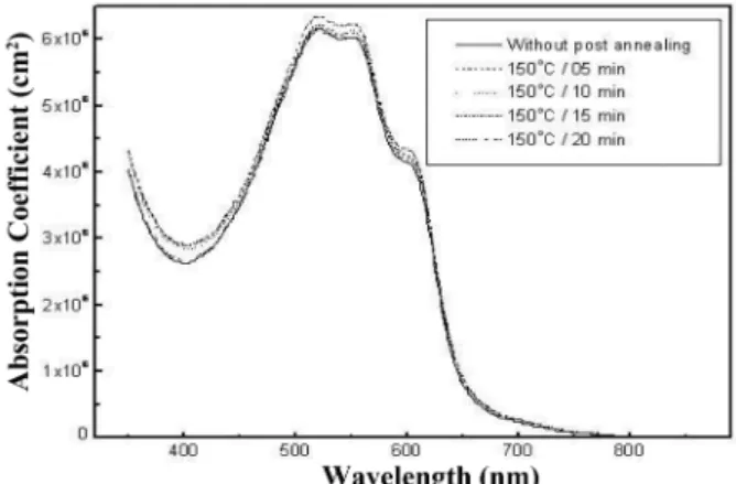
Fig. 3
는후속열처리전,
후의흡광계수의변화를보여주고 있다
.
본 연구에서 측정된UV-vis
특성에서는PCBM
의흡광도는측정되지않았으며, P3HT
의흡광계수만후속열처리시간이
5
분에서15
분으로증가할수록P3HT
의흡광계수는6.16
×10
6에서6.33
×10
6(520 nm)
으로다소증가하는경향을보였다
.
그러나20
분의후속열처리시간에서는
6.13
×10
6으로흡광계수가오히려낮아지는경향을보였다
.
Fig. 4
는후속열처리온도150
oC
에서열처리시간에따른
P3HT:PCBM
광활성층의XRD pattern
을보여준다.
열처리조건에상관없이
P3HT:PCBM
은2
θ=5.3
o(degree)
에Fig. 2.
The short circuit current density versus open circuit voltage (J
SC-V
OC) characteristics of polymer solar cells at various P3HT:PCBM concentrations.
Fig. 3.
The optical absorption coefficient of P3HT donor films with and without post annealing treatment at the time range from 5 to 20 min.
Fig. 4.
The XRD pattern of P3HT:PCBM active layer films with and without post annealing.
Fig. 5.
The short circuit current density
versusopen circuit voltage
(J
SC-V
OC) characteristics of solar cells with and without post
annealing treatments.
서
(100)
방향의결정피크(peak)
가관찰되었다.
Fig. 5
에서는활성층의후속열처리에따른유기박막태양전지의전기적특성을보여준다
.
열처리이전에비하여후속열처리 시간이
15
분으로 증가할수록J
SC와V
OC는4.7 mA/cm
2, 0.48 V
에서7.8 mA/cm
2, 0.55V
로증가하였고,
이때최대광변환효율은
0.97%
에서2.0%
로증가하였다.
후속열처리시간이증가할수록
J
SC 값이증가하는이유는Fig. 2
에서나타났듯이열처리에의하여P3HT
의흡광도가증가하면서박막내에전자
-
정공쌍의발생을증가시켜서캐리어의이동도가증가하였기때문이다
. 20
분의후속열처리에서는
Voc
는0.57 V
로증가하였지만,
전류밀도는6.0 mA/cm
2으로다소감소하였다.
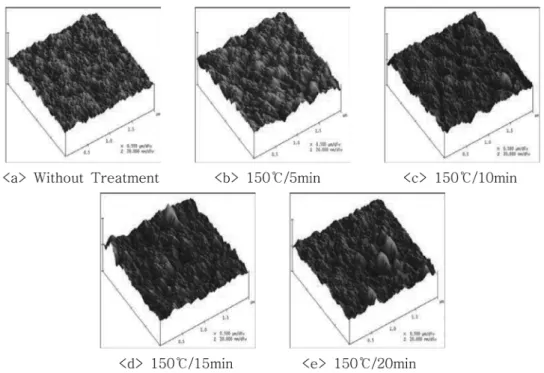
Fig. 6
은P3HT:PCBM
활성층의후속열처리에따른유기박막태양전지의
AFM
표면형상이미지를보여준다.
열처리이전에비하여후속열처리시간이증가할수록
rms
값은
0.90, 1.30, 1.33, 1.72, 1.87 nm
로점차증가하였다.
이것은
exciton
확산길이에영향을미치는특징적인요소로서열처리시간이증가할수록광활성층과전극사이의면 적을증가하게하여
Voc
의계속적인증가를나타낸다.
하지만
Table 1
에서보는바와같이열처리시간이15
분에서20
분으로증가하였을때Voc
의증가보다흡광계수의감소로인한
Jsc
와F.F
의감소로열처리효율은오히려감소하는것을볼수있다
.
4. 결 론
본연구에서는전자도너로
P3HT
와억셉터로PCBM
을톨루엔으로
0.5 wt%
의 농도로 용해한후, Glass/ITO/
PEDOT:PSS/P3HT-PCBM/Al
구조를갖는유기박막태양전지소자를제작하여후속열처리에의한소자의전기적 특성변화를조사하였다
. P3HT
와PCBM
의교반농도가4:4 wt%
에서J
sc, V
OC, FF, PCE
의값이 각각4.7 mA/cm
2, 0.48 V, 43.1%, 0.97%
로최적의소자특성을나타내었다.
최적의특성을갖는소자에대하여
150
oC
에서5
분, 10
분
, 15
분, 20
분간후속열처리를실시한후소자의특성에미치는영향을조사하였다
.
후속열처리를통하여소자의전기적특성은향상되는경향을보였다
.
특히P3HT
박막의흡광계수가커지면서광활성층에서캐리어의발생확 률이높아지고박막내캐리어의이동도가증가하여태양 전지소자의
J
SC특성은향상되었다.
또한후속열처리에의해광활성층과
Al
전극간의계면특성의향상으로누설전류특성이향상되면서
V
OC특성의향상을가져온것으로판단된다
.
후속열처리조건이150
oC
/15min
에서가장우수한특성이나타났으며
,
이때J
SC, V
OC, FF, PCE
는7.8 mA/cm
2, 0.55 V, 47%, 2.0%
로각각나타났다.
Fig. 6.
Atomic force microscope(AFM) Images of the P3HT:PCBM active layer with and without post annealing treatments.
Table 1.
The electrical properties of the polymer solar cells with and without post annealing treatments
I
sc(mA) J
sc(mA/cm
2) V
oc(v) F.F
(%) PCE
(%) Without
Treatment 0.19 4.7 0.475 43.1 0.97
150
oC/5min 0.26 6.4 0.505 49.6 1.6
150
oC/10min 0.26 6.4 0.505 51.6 1.7
150
oC/15min 0.31 7.8 0.545 47.0 2.0
150
oC/20min 0.24 6.0 0.566 41.9 1.4
감사의 글
이연구는
2009
년도단국대학교교책중점연구기관지원으로연구되었으며