http://dx.doi.org/10.5369/JSST.2017.26.4.223 pISSN 1225-5475/eISSN 2093-7563
CMOS Image Sensor with Dual-Sensitivity Photodiodes and Switching Circuit for Wide Dynamic Range Operation
Jimin Lee
1, Byoung-Soo Choi
1, Myunghan Bae
1, Sang-Hwan Kim
1, Chang-Woo Oh
2, and Jang-Kyoo Shin
1+Abstract
Conventional CMOS image sensors (CISs) have a trade-off relationship between dynamic range and sensitivity. In addition, their sen- sitivity is determined by the photodiode capacitance. In this paper, CISs that consist of dual-sensitivity photodiodes in a unit pixel are proposed for achieving wide dynamic ranges. In the proposed CIS, signal charges are generated in the dual photodiodes during inte- gration, and these generated signal charges are accumulated in the floating-diffusion node. The signal charges generated in the high-sen- sitivity photodiodes are transferred to the input of the comparator through an additional source follower, and the signal voltages converted by the source follower are compared with a reference voltage in the comparator. The output voltage of the comparator deter- mines which photodiode is selected. Therefore, the proposed CIS composed of dual-sensitivity photodiodes extends the dynamic range according to the intensity of light. A 94 × 150 pixel array image sensor was designed using a conventional 0.18 µm CMOS process and its performance was simulated.
Keywords: CMOS image sensor, Dual-sensitivity photodiodes, Switching circuit, Wide dynamic range
1. INTRODUCTION
CMOS image sensors (CISs) are widely used in security systems, digital single lens reflex (DSLR) cameras, medical devices, and mobile devices [1-8]. The main performance requirements of the CIS are high sensitivity, high resolution, low noise, and wide dynamic range (WDR). Among these performance parameters, WDR is a very important parameter for CISs [9-13]. There are several techniques for obtaining WDR, such as multiple sampling, linear-logarithmic response, or by using a lateral overflow integration capacitor (LOFIC) [14]. The use of dual-sensitivity photodiodes in charge-coupled device (CCD) image sensors had previously been proposed for achieving WDR [15]. However, this method suffers from slow processing speed because of the complex digital signal processing (DSP) circuit.
In this paper, we propose a WDR CIS that uses dual-sensitivity photodiodes with a comparator and switching circuit without DSP.
The proposed CIS has a higher processing speed than the CCD image sensors because the image signal processing circuit is simple.
2. DESIGN
2.1 Operation principle
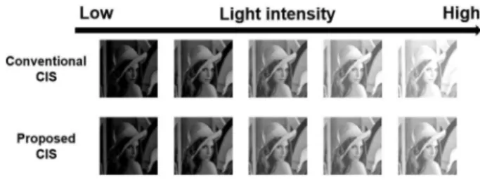
Fig. 1 shows the concept of the proposed CMOS image sensor. Noticeable differences can be observed between the images of the conventional CIS and the proposed CIS.
Compared to the conventional CIS, the proposed CIS exhibits a clearer image at a higher light intensity by using additional circuits. Fig. 2 shows the schematic of the proposed CIS. In the proposed CIS, two photodiodes with different sensitivities are
1
School of Electronics Engineering, Kyungpook National University, 80 Deahakro, Buk-gu, Daegu 702-701, Korea
2
Department of Sensor and Display Engineering, Kyungpook National University, 80 Deahakro, Buk-gu, Daegu 702-701, Korea
+