• 검색 결과가 없습니다.

Wide Dynamic Range CMOS Image Sensor with Adjustable Sensitivity Using Cascode MOSFET and Inverter

N/A
N/A
Protected

Academic year: 2021

Share "Wide Dynamic Range CMOS Image Sensor with Adjustable Sensitivity Using Cascode MOSFET and Inverter"

Copied!
5
0
0

로드 중.... (전체 텍스트 보기)

전체 글

(1)

http://dx.doi.org/10.5369/JSST.2018.27.3.160 pISSN 1225-5475/eISSN 2093-7563

Wide Dynamic Range CMOS Image Sensor with Adjustable Sensitivity Using Cascode MOSFET and Inverter

Donghyun Seong, Byoung-Soo Choi, Sang-Hwan Kim, Jimin Lee, and Jang-Kyoo Shin

+

Abstract

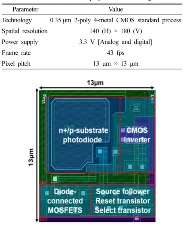
In this paper, a wide dynamic range complementary metal-oxide-semiconductor (CMOS) image sensor with the adjustable sensitivity by using cascode metal-oxide-semiconductor field-effect transistor (MOSFET) and inverter is proposed. The characteristics of the CMOS image sensor were analyzed through experimental results. The proposed active pixel sensor consists of eight transistors operated under various light intensity conditions. The cascode MOSFET is operated as the constant current source. The current generated from the cascode MOSFET varies with the light intensity. The proposed CMOS image sensor has wide dynamic range under the high illu- mination owing to logarithmic response to the light intensity. In the proposed active pixel sensor, a CMOS inverter is added. The role of the CMOS inverter is to determine either the conventional mode or the wide dynamic range mode. The cascode MOSFET let the current flow the current if the CMOS inverter is turned on. The number of pixels is 140 (H) × 180 (V) and the CMOS image sensor architecture is composed of a pixel array, multiplexer (MUX), shift registers, and biasing circuits. The sensor was fabricated using 0.35 µm 2-poly 4-metal CMOS standard process.

Keywords: CMOS image sensor, Wide dynamic range, Logarithmic response, Adjustable sensitivity.

1. INTRODUCTION

Recently, developments of the CMOS image sensors have received increased attention. Above all, the dynamic range of CMOS image sensors is important in order to recognize the object exactly regardless of the light intensity. There are many techniques for the wide dynamic range operation of CMOS image sensors. These include the mid-reset technique during exposure time, lateral overflow integration capacitor, sensitivity- controllable pixel, multiple-sampling, and so on. [1-7] However, these techniques are limited to the dynamic range for sensing in extremely high illumination conditions. Therefore, the logarithmic CMOS image sensor is suitable to capture images in high illumination condition.

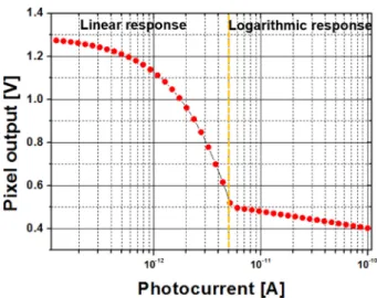
In the logarithmic CMOS image sensor, the pixel output voltage responds exponentially to the light intensity. Thus, the dynamic

range of the logarithmic CMOS image sensor is extremely wide.

The logarithmic operation is performed using the cascode MOSFET. By using the reference voltage applied to the cascode MOSFET, the pixel output voltage is affected by the constant current from the cascode MOSFET. [8] However, the sensitivity of the pixel array is controlled at the same time. The pixel array of the logarithmic CMOS image sensor has the same sensitivity.

The disadvantage of the logarithmic CMOS image sensor is that the sensitivity changes at low illumination conditions. To solve this problem, the CMOS inverter circuit is added to the unit pixel.

The CMOS inverter circuit decides the switching point called knee point which is the conversion point between the linear mode and wide dynamic range mode. If the cascode MOSFET is off, the pixel is in the linear mode. Otherwise, the pixel is in the logarithmic mode. The pixel array of the proposed CMOS image sensor has different sensitivity according to the light intensity.

In this paper, the active pixel sensor of the proposed CMOS image sensor consists of three circuit blocks. First, a cascode MOSFET is included for the logarithmic response according to the light intensity. Second, a CMOS inverter is included for the switching operation. Finally, a three-transistor active pixel sensor structure is used. Among them, the CMOS inverter and cascode MOSFET are the key-elements for adjustable sensitivity in response to the high illumination condition. The rest of the paper is organized as follows. The operating principle of the logarithmic School of Electronics Engineering, Kyunpook National University, 80

Daehakro, Bukgu, Daegu 41566, Korea

+

Corresponding author: [email protected] (Received: May. 24, 2018, Accepted: May. 30, 2018)

This is an Open Access article distributed under the terms of the Creative Commons Attribution Non-Commercial License(http://creativecommons.org/

licenses/bync/3.0) which permits unrestricted non-commercial use, distribution,

and reproduction in any medium, provided the original work is properly cited.

(2)

CMOS image sensor is introduced and simulation results are shown in Section 2. The experimental results are compared to the simulation data in Section 3. Finally, concluding remarks are presented in Section 4.

2. SENSOR CHARACTERISTICS

2.1 Operation of the proposed CMOS image sensor

The schematic diagram of the proposed active pixel sensor is shown in Fig. 1. There are two parts for the operation of the wide dynamic range mode. First, the CMOS inverter is located in each pixel and the input gate is connected to the n+/p-substrate photodiode junction. The cascode MOSFET is connected to guarantee the logarithmic response according to the light intensity.

There are seven n-type MOSFET and one p-type MOSFET for each pixel. In Fig. 1, M1, M2, and M3 are the transistors for the reset operation, amplification, and select operation, respectively.

The CMOS inverter consists of M4 and M5 transistors. The output node of the CMOS inverter is connected to the gate of the M6 transistor for applying the signal to change the mode. Finally, the M7 and M8 transistors are used for the cascode MOSFET.

When the photodiode is exposed to the light, its voltage decreases.

The input voltage of the CMOS inverter also decreases while exposed to light. If the output voltage of the CMOS inverter

changes from logically “0” to “1”, then the M6 transistor is turned on and the voltage of the source node of M6 is applied to the the M7 transistor. At the same time, the M7 and M8 transistors are turned on and the flowing current induces the logarithmic response of the sensor. The output voltage which is the source node of M3 depends on the V

REF

voltage. Therefore, the current by the cascode MOSFET changes after adjusting the V

REF

voltage.

2.2 Simulation result

The simulation was conducted to check whether the proposed method for the wide dynamic range CMOS image sensor is effective. First, the photodiode in Fig. 1 is replaced with the SPICE model for the simulation. [9] In Fig. 2, the capacitor, constant current source, and photodiode are used for modeling the active pixel sensor. The current source represents the amount of photocurrent generated by the light, and the capacitor is considered as the n+/p-substrate photodiode capacitance.

Fig. 3 shows the timing diagram to explain the pixel operation with wide dynamic range mode. The reset operation that eliminates the charge that accumulates in the photodiode, the electric signal is generated within the exposure time.

When the V

PD

has the same voltage value of half of the CMOS inverter power supply voltage, the output voltage of the CMOS inverter changes from logically “0” and the wide dynamic range

Fig. 1. Schematic diagram of the proposed active pixel sensor.

Fig. 2. SPICE model of the photodiode for the simulation.

Fig. 3. Timing diagram of the active pixel sensor operation.

(3)

mode is operated as the logarithmic response.

Fig. 4 shows the simulation result of the pixel output voltage. It indicates that the pixel output voltage responds according to the photocurrent. This simulation result is based on the 30 frames per second (fps) condition and the photodiode capacitance value of 50 fF. At photocurrent less than 5 pA, the linear response is shown in the pixel output voltage as the photocurrent rises. On the other hand, the logarithmic response is shown when the photocurrent is greater than 5 pA because the CMOS inverter is turned on and the current flows through the cascode MOSFET.

The transient simulation result of the pixel response is described in Fig. 5. When the sensor is exposed to the low illumination condition. The wide dynamic range CMOS image sensor has a linear output response. However, in the high illumination condition, the wide dynamic range CMOS image sensor has a

logarithmic response according to the light intensity by turning on the CMOS inverter. In Fig. 5, the transient simulation result of the pixel response are shown. There are four simulation results depending on the photocurrent intensity. The logarithmic response is shown when the 10 pA photocurrent flows into the active pixel sensor. The linear response is also shown when the 10 fA, 1 pA, and 5 pA photocurrents flow into the active pixel sensor because the CMOS inverter is off. After the CMOS inverter is turned on, the pixel output voltage is in steady-state having a specific value.

2.3 Architecture of the CMOS image sensor

The proposed CMOS image sensor consists of a pixel array, vertical scanner, MUX, horizontal scanner and biasing circuit.

First, the pixel array with 140 rows and 180 columns is located at the center of the fabricated chip. The shift registers based on the flip-flop were located for the vertical and the horizontal direction scanning. Finally, MUX were located with a column-parallel structure and the analog outputs which have the pixel output voltage pass through the chip pad.

The active pixel sensor proposed in this paper is based on the conventional three-transistor type with five extra transistors for wide dynamic range operation. The pixel pitch of 13 µm × 13 µm is assigned in the vertical and horizontal directions. The n+/p- substrate photodiode is exposed to the light directly and signal electrons are generated owing to the incident lights.

As described in Table 1, the total number of pixels is 25,200 and the proposed CMOS image sensor is operated by either the conventional mode or wide dynamic range mode. The power Fig. 4. Simulation result of the pixel output voltage according to the

quantity of the photocurrent.

Fig. 5. Transient simulation result of pixel response.

Fig. 6. Block diagram of the proposed CMOS image sensor.

(4)

supply voltage is 3.3 V for the analog and digital blocks. The frame rate is 43 fps. The chip sizes are 2.6 mm and 4.0 mm.

3. RESULTS AND DISCUSSION

To compare the simulation and the experimental results, the measurement system was installed with the printed circuit board and external integration circuit devices. The reset and select pulse were generated from the field programmable gate array (FPGA) device, and the pulse width was controlled by the FPGA code.

The printed circuit board is shown in Fig. 8. At the center of the printed circuit board, the camera lens is mounted. The reference voltage and current for operating the CMOS image sensor were applied to the sensor using the external voltage and current source.

The output voltage of the CMOS image sensor was converted to digital code through the 8-bit external analog to digital converter device. Then, the acquired digital output is displayed through the Microsoft foundation class library program.

Fig. 9 shows the measured pixel output voltage according to the light intensity. When the light intensity is less than 500 lux, the pixel output voltage responds to the linear mode. On the other

hand, the logarithmic response is shown when the light intensity is greater than 500 lux because the CMOS inverter is turned on.

The logarithmic response depends on the knee point. The result shows that the V

REF

voltage at the logarithmic response changes the pixel output voltage. In the logarithmic operation, the pixel output voltage depends on V

REF

. If V

REF

is 0.6 V, then the current due to the cascode MOSFET is not effective. However, if V

REF

is 2.4 V, then the pixel output voltage shows the logarithmic response. Therefore, the CMOS image sensor operates in the logarithmic mode when the current from the cascode MOSFET is dominant. The measured results prove that the wide dynamic range operation is dependent on the V

REF

voltage.

The knee point between the linear mode and logarithmic mode can be controllable by changing the power supply voltage of the CMOS inverter. If the power supply voltage of the CMOS inverter is low, then the knee point changes under the higher illumination condition. On the other hand, if the power supply voltage is high, the knee point changes under the lower illumination condition. By changing the knee point, the sensitivity at the specific light intensity is controlled.

Table 1. Characteristics of the proposed CMOS image sensor.

Parameter Value

Technology 0.35 µm 2-poly 4-metal CMOS standard process Spatial resolution 140 (H) × 180 (V)

Power supply 3.3 V [Analog and digital]

Frame rate 43 fps

Pixel pitch 13 µm × 13 µm

Fig. 7. Layout of the active pixel sensor.

Fig. 8. Printed circuit board for the measurement.

Fig. 9. Measured pixel output voltage according to the light intensity.

(5)

4. CONCLUSION

A wide dynamic range CMOS image sensor with adjustable sensitivity by using the cascode MOSFET and the inverter was proposed. By using the CMOS inverter, either the wide dynamic range mode or conventional mode was selected by switching the operation according to the light intensity. The proposed CMOS image sensor architecture includes a pixel array, MUX, shift registers and biasing circuits. The CMOS image sensor was fabricated using 0.35 µm 2-poly 4-metal CMOS standard process.

The experiment was conducted to measure the characteristics of the CMOS image sensor. The results were compared for the wide dynamic range mode and conventional mode. The pixel output voltage shows that the CMOS image sensor performed with wide dynamic range operation by using the cascode MOSFET and the inverter. Moreover, the pixel output voltage was dependent on the logarithmic operation by changing the reference voltage. As a result, the logarithmic response was operated for the wide dynamic range operation in the high illumination condition.

ACKNOWLEDGMENT

This work was supported by Integrated Circuit Design Education Center (IDEC) in Korea, the BK21 Plus project funded by the Ministry of Education, Korea (21A20131600011) and Samsung Electronics Co., Ltd.

REFERENCES

[1] M. Bigas, E. Cabruja, J. Forest, and J. Salvi, “Review of CMOS image sensors”, Microelectron. J., Vol. 37(2), pp.

433-451, 2006.

[2] E. Fossum, “CMOS image sensors: Electronic camera on a chip”, IEEE Trans. Electron Devices, Vol. 44(10), pp. 1689- 1698, 1997.

[3] J. Park, M. Mase, S. Kawahito, M. Sasaki, Y. Wakamori and Y. Ohta, “A 142dB Dynamic Range CMOS Image Sensor with Multiple Exposure Time Signals”, IEEE Asian Solid- State Circuits Conf., pp. 85-88, Hsinchu, Taiwan, 2005.

[4] J. Rhee and Y. Joo, “Dual-mode wide dynamic range CMOS active pixel sensor”, Electron. Lett., Vol. 41(24), pp.

1322-1323, 2005.

[5] N. Akahane, S. Sugawa, S. Adachi, K. Mori, T. Ishiuchi, and K. Mizobuchi, “A Sensitivity and Linearity Improve- ment of a 100-dB Dynamic Range CMOS Image Sensor Using a Lateral Overflow Integration Capacitor”, IEEE J.

Solid-State Circuits, Vol. 41(4), pp. 851-858, 2006.

[6] J. Nakamura, Image Sensors and Signal Processing for Dig- ital Still Cameras, CRC Press, Florida, pp. 147-148, 2006.

[7] S. Lee and K. Yang, “A Novel Self-Adaptive Photosensing Active-Pixel Structure with Tunable Sensitivity for High Performance CMOS Image Sensors”, IEEE Sens. Conf., pp.

299-302, Daegu, Korea, 2006.

[8] M. Bae, B.-S. Choi, S.-H. Jo, H.-H. Lee, P. Choi, and J.-K.

Shin, “A Linear-Logarithmic CMOS Image Sensor with Adjustable Dynamic Range,” IEEE Sens. J., Vol. 16(13), pp. 5222-5226, 2016.

[9] D. Cheung, “CMOS Active Pixel Sensor Designs for Fault

Tolerance and Background Illumination Subtraction”,

Simon Fraser University, Burnaby, pp. 120-122, 2005.

수치

Fig. 1. Schematic diagram of the proposed active pixel sensor.
Fig. 4 shows the simulation result of the pixel output voltage. It indicates that the pixel output voltage responds according to the photocurrent
Table 1. Characteristics of the proposed CMOS image sensor.

참조

관련 문서

- 각종 지능정보기술은 그 자체로 의미가 있는 것이 아니라, 교육에 대한 방향성과 기술에 대한 이해를 바탕으로 학습자 요구와 수업 맥락 등 학습 환경에 맞게

Taubin, “The QBIC Project: Querying Image by Content using Color, Texture and Shape,” Proceedings of SPIE Storage and Retrieval for Image and Video Databases, pp.. Pala,

produces a magnetic field which can be guided by a magnetic yoke to a linear Hall sensor; the output of the sensor is proportional to the electric current..

Wide Dynamic Range Auto On/Off Mode The wide dynamic range can be set to be automatically switched ON/OFF in accordance with the intensity difference obtained by dividing an

SigmaNEST 펀칭 파워팩 제품 관리, 자동 다이나믹™ 배 열 및 펀칭 툴 관리를 갖춘 터렛 펀칭 프로그래밍을 위한 가장 완벽하고 최적화된

6.56 Usinga computer analysis, investigate the effect of the transistor parameters  and on the small-signal voltage gain and output resistance of the source-follower

This paper proposes a histogram equalization technique with AGC (Automatic Gain Control) to extend the image enhancement range.. It is designed using VHDL (VHSIC Hardware

Existing method has applied the size of the target to the virtual character by measuring manually, but now using Kinect sensor the motion data file can