• 검색 결과가 없습니다.

Linear-logarithmic Active Pixel Sensor with Photogate for Wide Dynamic Range CMOS Image Sensor

N/A
N/A
Protected

Academic year: 2021

Share "Linear-logarithmic Active Pixel Sensor with Photogate for Wide Dynamic Range CMOS Image Sensor"

Copied!
4
0
0

로드 중.... (전체 텍스트 보기)

전체 글

(1)

79 J. Sensor Sci. & Tech. Vol. 24, No. 2, 2015 Journal of Sensor Science and Technology

Vol. 24, No. 2 (2015) pp. 79-82 http://dx.doi.org/10.5369/JSST.2015.24.2.79 pISSN 1225-5475/eISSN 2093-7563

Linear-logarithmic Active Pixel Sensor with Photogate for Wide Dynamic Range CMOS Image Sensor

Myunghan Bae, Sung-Hyun Jo, Byoung-Soo Choi, Pyung Choi, and Jang-Kyoo Shin

+

Abstract

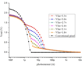
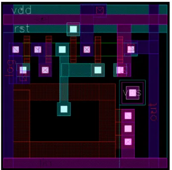
This paper proposes a novel complementary metal oxide semiconductor (CMOS) active pixel sensor (APS) and presents its per- formance characteristics. The proposed APS exhibits a linear-logarithmic response, which is simulated using a standard 0.35-µm CMOS process. To maintain high sensitivity and improve the dynamic range (DR) of the proposed APS at low and high-intensity light, respec- tively, two additional nMOSFETs are integrated into the structure of the proposed APS, along with a photogate. The applied photogate voltage reduces the sensitivity of the proposed APS in the linear response regime. Thus, the conversion gain of the proposed APS changes from high to low owing to the addition of the capacitance of the photogate to that of the sensing node. Under high-intensity light, the integrated MOSFETs serve as voltage-light dependent active loads and are responsible for logarithmic compression. The DR of the proposed APS can be improved on the basis of the logarithmic response. Furthermore, the reference voltages enable the tuning of the sensitivity of the photodetector, as well as the DR of the APS.

Keywords: CMOS image sensor, Linear-logarithmic response, Photogate, Dynamic range

1. INTRODUCTION

Recently, complementary metal oxide semiconductor (CMOS) active pixel sensors (APSs) have been used in a wide variety of applications including digital cameras and mobile phones. The structure of an APS is typically either a three-transistor (3-Tr) APS or a four-transistor (4-Tr) APS. A pinned-photodiode-based 4-Tr APS structure is preferred over a 3-Tr structure in an APS because the former offers performance advantages such as low dark current and high sensitivity [1]. However, the pinned- photodiode-based 4-Tr APS suffers from disadvantages such as a low fill factor resulting from the use of additional transistors, a low dynamic range (DR) associated with a low well capacity, and high cost since a modification in the conventional CMOS process is required [2-3].

Various approaches have been proposed to realize an APS with high sensitivity and a wide DR [4-10]. Certain equipment for

high-sensitivity applications uses photomultiplier tubes or charge coupled devices (CCDs). However, these photodetectors consume a large amount of power and cannot be integrated with CMOS logic circuits.

Logarithmic sensors are more likely to exhibit a wide DR at high illumination owing to the compression of an image signal.

However, conventional logarithmic sensors operating in a sub- threshold region suffer from low sensitivity at low-intensity light.

The quality of the resulting output image of the logarithmic sensor is degraded by mismatches between the individual pixels in each sensor.

A multiple sampling technique provides a wide DR, without the need for pixel modification. On the other hand, a conventional multiple sampling method requires additional frame memory circuits and an image synthesis process [11].

In this paper, we propose a novel CMOS image sensor with a wide DR. The proposed APS exhibits a linear-logarithmic response, and its DR can be modified by adjusting the reference voltage. Further, the proposed APS has been designed and simulated using a 0.35-μm 2-poly 4-metal CMOS process.

2. STRUCTURE AND OPERATION OF PROPOSED APS

2.1 Structure

School of Electronics Engineering, Kyungpook National Unversity

IT3 301, Kyungpook National Unversity, 80 Daehakro, Bukgu, Daegu, 702- 701, Korea

+

Corresponding author: [email protected]

(Received : Dec. 29, 2014, Revised : Mar. 25, 2015, Accepted : Mar. 25, 2015)

This is an Open Access article distributed under the terms of the Creative Commons Attribution Non-Commercial License(http://creativecommons.org/

licenses/bync/3.0) which permits unrestricted non-commercial use, distribution,

and reproduction in any medium, provided the original work is properly cited.

(2)

Myunghan Bae, Sung-Hyun Jo, Byoung-Soo Choi, Pyung Choi, and Jang-Kyoo Shin

J. Sensor Sci. & Tech. Vol. 24, No. 2, 2015 80 The schematic of the proposed APS shown in Fig. 1 is an equivalent circuit diagram of the proposed APS structure. As shown in this figure, a positive bias voltage (V

lin

) is applied at the photogate to achieve the desired second linear operation and controllability of the APS. The structure of the new APS is similar to that of a conventional 3-Tr APS. The photosensing component of the proposed structure comprises both a photogate region and a photodiode region, as shown in Fig. 1.

The APS is surrounded by the photogate such that it is isolated from the defective field oxide region. In addition, since the proposed APS structure comprises a series of transistors (M4 and M5) whose gates are connected to the drains, yields a logarithmic response. The pixel response can simply be adjusted by tuning the point of transition between the linear and the logarithmic domains through the appropriate setting of a reference voltage (V

log

).

2.2 Operational principle

The proposed APS exhibits two linear responses (first and second linear responses) owing to the fact that the photogate causes an increase in the sensing node’s capacitance. The first linear response is a conventional response, which is identical to that of a conventional pixel sensor with a photodiode. From this response, it can be inferred that the proposed APS displays high sensitivity at low-intensity light. The detailed operational principle of the proposed APS is described as follows (1 −3). We assume that the operation of the APS is identical to that of the conventional 3-Tr APS. First, the voltage of the sensing node (V

PD

) increases to the reset level (V

rst

) with a biased V

lin

given that

(V

lin

−V

t

) < V

rst

, where V

t

is the threshold voltage of the photogate.

During the exposure interval, V

PD

becomes less than V

rst

due to the light illumination. In this region, the capacitance of the photodiode (C

PD

) is electrically disconnected from that of the photogate (C

PG

) as a consequence of the lack of formation of the photogate channel. Hence, it can be confirmed that the proposed pixel sensor exhibits high sensitivity in low-intensity light. When the value of V

PD

is less than V

lin

-V

t

and greater than V

log

-2V

t

, a photogate channel is formed and C

PG

is connected to C

PD

through this channel. Thus, the total capacitance of the sensing node becomes equal to C

PD

+ C

PG

. For this reason, the sensitivity of the proposed pixel sensor decreases significantly. When V

PD

is further decreased to less than V

log

-2V

t

, the proposed APS reveals a logarithmic response as the integrated MOSFETs are switched on.

Furthermore, V

lin

and V

log

can be controlled to adjust the starting point of the second linear response and the logarithmic response.

Moreover, the value of V

lin

must be higher than that of V

log

to achieve the desired operation. Otherwise, the second linear response will begin to fade when the value of V

log

becomes equal to V

lin

. In summary, the operation of the proposed APS can be described by the following equations.

(1) (1st linear response)

(2) (2nd linear response)

(3) (logarithmic response)

3. SIMULATION AND DESIGN

3.1 Simulation

The proposed APS is simulated using Cadence Spectre with parameters of the standard 0.35-µm CMOS process. Fig. 2 shows the simulation results of the output swing for the varied photocurrent at an exposure time of 30 ms. The output of the proposed APS has an decreasing slope. At a low photocurrent, the output voltage waveform of the proposed APS is similar to that of the conventional pixel sensor, showing no electrical disturbance.

At a moderate photocurrent level, a change in the capacitance of the sensing node can result in the generation of the second linear

V

rst

≥ V

PD

> V

lin

– V

t

:V

PD

Δ Q C

PD

---

=

V

lim

– V

t

≥ V

PD

> V

log

– 2 V ⋅

t

:V

PD

Δ Q C

PD

+ C

PG

---

=

V

log

– 2 V ⋅

t

≥ V

PD

:V

PD

V

log

2 kT --- q i

DS

i

o

---

⎝ ⎠ ⎛ ⎞

⋅ ⋅ ln –

= Fig. 1. Schematic of the proposed APS.

I 2 I

(3)

Linear-logarithmic Active Pixel Sensor with Photogate for Wide Dynamic Range CMOS Image Sensor

81 J. Sensor Sci. & Tech. Vol. 24, No. 2, 2015 response because of the formation of the photogate channel. At

very high photocurrent values, the APS displays a logarithmic response. The simulation results agree with the theoretical results obtained using the defined equations. Consequently, without modifying any process, the proposed APS presents improvements in terms of DR and sensitivity.

Fig. 3 shows the simulation results of the variation in the output voltage of the proposed APS as a function of V

lin

. The capacitance of the sensing node leads to the generation of the second linear response. The sensitivity of the proposed APS can be tuned and controlled at different photocurrent levels by varying V

lin

. When V

lin

= 1.8 V, the output swing does not exhibit the second linear response; instead, it immediately starts to display a logarithmic response.

Fig. 4 illustrates the simulation results of the variation in the

output voltage of the proposed APS as a function of V

log

. These results indicate that both the high-intensity sensitivity and the DR can be significantly improved thanks to the logarithmic response.

V

log

can be changed in order to set the origin of the logarithmic response. Although the conventional pixel is already saturated, the proposed one does not yet saturate until the photocurrent value of 10 nA, as shown Fig. 4. Furthermore, the APS is able to detect a photocurrent from 100 fA to 10 nA. However, the conventional APS can detect the photocurrent only from 100 fA to 3pA. Based on the DR formula (4), it is found that the DR of the conventional APS is approximately 30 dB and that of the proposed APS is greater than 100 dB. To conclude, the DR of the proposed APS is significantly increased by the effect of the photogate, and its logarithmic operation.

(4)

3.2 Design

The proposed APS is designed using a standard 0.35-µm CMOS process. Fig. 5 shows the layout of the APS with the dimensions 13 µm × 13 µm. These dimensions are used since it is difficult to further reduce the size of the column-parallel readout circuits in the 0.35-µm CMOS process. Advanced CMOS technologies can be used to design an APS chip with even smaller dimensions. Moreover, a prototype sensor array of the proposed APS is designed with a resolution of 120 × 160. A prototype image sensor comprises a pixel array, a V-scanner, an H-scanner, and column multiplexor. This sensor has dimensions of 2 mm ×

DR :20 I

max

I

min

---

⎝ ⎠

⎛ ⎞ dB [ ]

⋅ log Fig. 2. Simulation results of the variation in the output voltage of the

proposed APS as a function of photocurrent (exposure time = 30 ms).

Fig. 3. Simulation results of the variation in the output voltage of the proposed APS as a function of V

lin

(V

log

= 1.8 V).

Fig. 4. Simulation results of the variation in the output voltage of the proposed APS as a function of V

log

(V

lin

= 3.3 V).

I 3 I

(4)

Myunghan Bae, Sung-Hyun Jo, Byoung-Soo Choi, Pyung Choi, and Jang-Kyoo Shin

J. Sensor Sci. & Tech. Vol. 24, No. 2, 2015 82 1.5 mm. In the future, the characteristics of this sensor will be evaluated.

4. CONCLUSIONS

In this paper, a novel, wide dynamic range APS that exhibits a linear-logarithmic response was proposed. At low-intensity light, both DR and linear sensitivity of the proposed APS improved owing to the capacitance condition of the photodetector.

Moreover, V

lin

was varied to adjust the origin of the second linear response. Finally, the pixel response was simply adjusted by tuning the transition point between the linear and the logarithmic domains through the appropriate setting of V

log

. In the future, a prototype of the proposed APS will be fabricated with a resolution of 120 × 160. Its characteristics will be evaluated and compared to the simulation results.

ACKNOWLEDGMENT

This work was supported by Samsung Electronics Co., Ltd., and Integrated Circuit Design Education Center (IDEC) in Korea.

REFERENCES

[1] H. Abe, “Device technologies for high quality and smaller pixel in CCD and CMOS image sensors”, IEDM Tech. Dig., pp. 989-992, 2004.

[2] K. Mabuchi, N. Nakamura, E. Funatsu, T. Abe, T. Umeda, T. Hoshino, R. Suzuki, and H. Sumi, “CMOS image sensors comprised of floating diffusion driving pixels with buried photodiode”, IEEE Journal of Solid-State Circuits, Vol. 39, No. 12, pp. 2408-2416, 2004.

[3] H. Takahashi, M. Kinoshita, K. Morita, T. Shirai, T. Sato, T.

Kimura, H. Yuzurihara, S. Inoue, and S. Matsumoto, “A 3.9-µm pixel pitch VGA format 10-b digital output CMOS image sensor with 1.5 transistor/pixel”, IEEE Journal of Solid-State Circuits, Vol. 39, No. 12, pp. 2417-2425, 2004.

[4] M. Ikebe, and K. Saito, “A Wide-Dynamic-Range Com- pression Image Sensor With Negative-Feedback Resetting”, IEEE Sensors Journal, Vol. 7, No. 5, pp. 897-904, 2007.

[5] G.G. Storm, J.E.D Hurwitz, D. Renshaw, K. M. Findlater, R.

K. Henderson and M. D. Purcell, “Combined linear-log- arithmic CMOS image sensor”, IEEE ISSCC Dig. Tech., pp.

112-116, 2004.

[6] T. Yamada, S. Kasuga, T. Murata, and Y. Kato, “A 140dB- Dynamic-Range MOS Image Sensor with In-Pixel Mul- tiple-Exposure Synthesis”, IEEE ISSCC Dig. Tech., pp. 50- 51, 2008.

[7] N. Akahane, R. Ryuzaki, S. Adachi, K. Mizobuchi and S.

Sugawa, “A 200dB Dynamic Range Iris-less CMOS Image Sensor with Lateral Overflow Integration Capacitor using Hybrid Voltage and Current Readout Operation”, IEEE ISSCC Dig. Tech., pp. 1161-1170, 2006.

[8] T. H. Hsu, Y. K. Fang, D. N. Yaung, J. S. Lin, S. G. Wuu, H. C. Chien, C. H. Tseng, C. S. Wang, S. F. Chen, C. Y. Lin, C. S. Lin, and T. H. Chou, “An effective method to improve the sensitivity of deep submicrometer CMOS image sen- sors”, IEEE Electron Device Letters, Vol. 26, pp. 547-549, 2005.

[9] Y. Chae, K. Choe, B. Kim, and G. Han, "Sensitivity con- trollable CMOS image sensor pixel using control gate over- laid on photodiode”, IEEE Electron Device Letters, vol. 28, pp. 495-498, 2007.

[10] M. Bae, S.-H. Jo, M. Lee, J.-Y. Kim, J. Choi, P. Choi, and J.-K. Shin, “A wide dynamic range CMOS image sensor based on a pseudo 3-transistor active pixel sensor using feedback structure”, Journal of Sensor Science and Tech- nology, Vol. 21, pp. 413-419 2012.

[11] M. Sasaki, M. Mase, S. Kawahito and Y. Tadokoro, “A wide-dynamic-range CMOS image sensor based on mul- tiple short exposure-time readout with multiple-resolution column-parallel ADC”, IEEE Sensors Journal, Vol. 7, No.

1, pp. 151-158, 2007.

Fig. 5. Layout of the proposed APS.

I 4 I

수치

Fig. 3. Simulation results of the variation in the output voltage of the proposed APS as a function of V lin  (V log  = 1.8 V).
Fig. 5. Layout of the proposed APS.

참조

관련 문서

Fluorescence Amplication and Development of VOCs Sensor Based on Anisotropic Porous Silicon Derivatives..

The purpose of the study is to develop a sensor data collection and monitoring system with database using IoT techrology and to apply the ststem to three

Wang, “Medium access control with a dynamic duty cycle for sensor networks,” IEEE Wireless Communications and Networking Conference, vol.. Dubendorfer,

Lee, Mechanism of micro crack sensor using electrohydrodynamic printing, Journal of Advanced Engineering and Technology.. Schubert, Inkjet Printing of Polymers:

In wireless sensor networks (WSNs), a transport protocol plays an important role of reliable transmission and congestion control.. The efficient design of

Park, “NDT of a nickel Inconel specimen using by the complex induced current - magnetic flux leakage method and linearly integrated hall sensor array”, Journal of the

Development of Naphtha Sensor Based on DBR Porous Silicon and Fluorescence Resonance Study between Silole1. and

Depth Sensor As a sensor to measure hydrostatic pressure of knowing the depth of the device.. Board 1,2 The performance of various sensors and controls to be able to use