1. INTRODUCTION
As CMOS technology scales down and pixel size is reduced for higher-resolution sensors, it is becoming more difficult to design high-performance CMOS image sensors (CISs). As the technology scales down, lower saturation level due to the small operation voltage and higher noise level due to the mismatch of the device makes the dynamic range a very significant problem. The CISs which currently dominate the image sensor market have a dynamic range of less than three orders of magnitude. Consequently, the response of these image sensors suffers from saturated parts of the captured image due to insufficient dynamic range [1-10]. To overcome these problems, several on-chip techniques have been proposed that can extend the dynamic range of a sensor. Several approaches have been
proposed to extend the dynamic range of CIS [11-15]. One method is to add a storage capacitor to the charge-sensing node depending on the light conditions. Another approach is sampling a charge-sensing node multiple times and constructing an image afterwards using fusion algorithms in the digital domain. The main disadvantage of these systems is the cost of the processing needed to synthesize the final image. Logarithmic response pixels have a wide dynamic range. Logarithmic pixels can be designed using a MOS transistor operating in the subthreshold region. The problem with logarithmic pixels is that the quality of the resulting output image is severely degraded by fixed pattern noise (FPN) caused by mismatches between the components of individual pixels in each sensor. In addition, the continuous nature of the operation for logarithmic sensors makes it impossible to use FPN reduction methods like the double sampling method and the correlated double sampling (CDS) circuit method.
In this paper, an approach for dynamic range extension using an NMOSFET switch and an additional photode- tector based on a conventional 3-transistor APS with a gate/body-tied PMOSFET-type photodetector is suggested.
The proposed pixel can choose the operating mode by the voltage of the transfer gate in the proposed pixel. Although the pixel size has been increased, the dynamic range was
1School of Electronics Engineering, Kyungpook National University, 1370 Sankyuk-dong, Buk-gu, Daegu 702-701, Korea
2Department of Sensor and Display Engineering, Kyungpook National University, 1370 Sankyuk-dong, Buk-gu, Daegu 702-701, Korea +Corresponding author: [email protected]
(Received : Oct. 11, 2012, Accepted : Oct. 23, 2012)
This is an Open Access article distributed under the terms of the Creative Commons Attribution Non-Commercial License(http://creativecommons.org/licenses/by- nc/3.0)which permits unrestricted non-commercial use, distribution, and reproduction in any medium, provided the original work is properly cited.
pISSN 1225-5475/eISSN 2093-7563
A Wide Dynamic Range CMOS Image Sensor Based on a Pseudo 3-Transistor Active Pixel Sensor Using Feedback Structure
Myunghan Bae
1, Sung-Hyun Jo
1, Minho Lee
1, Ju-Yeong Kim
1, Jinhyeon Choi
2, Pyung Choi
1, and Jang-Kyoo Shin
1, +Abstract
A dynamic range extension technique is proposed based on a 3-transistor active pixel sensor (APS) with gate/body-tied p-channel metal oxide semiconductor field effect transistor (PMOSFET)-type photodetector using a feedback structure. The new APS consists of a pseudo 3-transistor APS and an additional gate/body-tied PMOSFET-type photodetector, and to extend the dynamic range, an NMOSFET switch is proposed. An additional detector and an NMOSFET switch are integrated into the APS to provide negative feedback. The proposed APS and pseudo 3-transistor APS were designed and fabricated using a 0.35-
Ïm 2-poly 4-metal standard complementary metal oxide semiconductor (CMOS) process. Afterwards, their optical responses were measured and characterized.
Although the proposed pixel size increased in comparison with the pseudo 3-transistor APS, the proposed pixel had a significantly extended dynamic range of 98 dB compared to a pseudo 3-transistor APS, which had a dynamic range of 28 dB. We present a proposed pixel that can be switched between two operating modes depending on the transfer gate voltage. The proposed pixel can be switched between two operating modes depending on the transfer gate voltage: normal mode and WDR mode. We also present an imaging system using the proposed APS.
Keywords : CMOS image sensor, Wide dynamic range, Gate/body-tied PMOSFET-type photodetector
significantly extended by feedback behavior using the output voltage of each pixel. The proposed pixel structure has been designed and fabricated using the 0.35- Ï m 2-poly 4-metal CMOS process. An imaging system using the proposed APS has also been implemented, and its characteristics have been measured.
2. OPERATIONAL PRINCIPLE
Fig. 1 shows a cross sectional view of the gate/body-tied PMOSFET-type photodetector [16-18], and Fig. 2 shows its symbol.
Fig. 3 shows the schematic and layout of the pseudo 3- transistor APS. The pseudo 3-transistor APS consists of a gate/body-tied PMOSFET-type photodetector with a transfer gate and a conventional 3-transistor APS. Fig. 4 shows the schematic and layout of the proposed pixel. The sensing node of the pseudo 3-transistor APS is connected to an additional gate/body-tied PMOSFET-type photodetector (PD
feedback) and an NMOSFET (M
4). The gate of M
4is connected to a source follower in the proposed pixel to enable the feedback. In low light, M
4is under the subthreshold region. After a certain charge accumulation period, M
4is gradually turned on due to the
increased output voltage, which is connected to the gate of M
4. During that time, the sensitivity slope is decreased due to the feedback current of M
4. When a positive voltage is applied to the gate relative to the source voltage of M
4, negative charges are induced in the underlying gate of M
4, by formation of a depletion region and a thin surface region containing mobile electrons. These induced electrons form the channel of M
4, and allow feedback current to flow from the source to the drain. There is significant current flow from the source to the drain of M
4. For this reason, the slope of the output voltage of the proposed pixel decreases, and the saturation of the sensing node is delayed, so that the dynamic range can be extended. The size of the proposed pixel is 13.6 ø 13.6 Ï m
2, which is slightly larger than the pseudo 3-transistor APS.
3. RESULTS AND DISCUSSION
3.1 Simulation and measurement of the proposed pixel
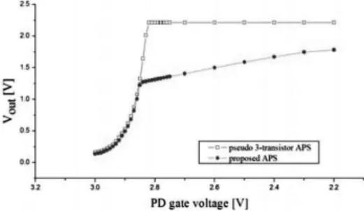
Fig. 5 shows the simulation results of the variation of the output voltage with the photodetector (PD) gate voltage,
Fig. 1. Cross sectional view of gate/body-tied PMOSFET-type photodetector.
Fig. 2. Symbol of the gate/body-tied PMOSFET type photode- tector.
Fig. 3. Schematic and layout of the pseudo 3-transistor APS.
Fig. 4. Schematic and layout of the proposed APS.
which is related to the light intensity in the pseudo 3- transistor APS and the proposed APS. The pseudo 3- transistor APS had a high sensitivity and linear response to light intensity, as shown in Fig. 5. However, saturation of the proposed pixel is delayed compared to the pseudo 3- transistor APS by the feedback of the proposed APS. This indicates an improvement of the dynamic range at high illumination.
Fig. 6 shows the measurement results of the variation of the output voltage with the light intensity in the pseudo 3- transistor APS and the proposed APS. The results are similar to the simulation results shown in Fig. 5. The pseudo 3-transistor APS was saturated with a high sensitivity at a low light intensity of 20 lux. The slope of the output voltage (V
out) of the proposed pixel was changed when V
outincreased above the threshold voltage of M
4. After M
4was turned-on at 20-lux light intensity, the slope of V
outchanged, because the photocurrent was then flowing into the sensing node. Thus, the saturation of the sensing node was delayed by this feedback. As shown in Fig. 6, the proposed pixel showed a significantly extended dynamic range of 98 dB, in contrast to the pseudo 3- transistor APS, which had a dynamic range of 28 dB.
Fig. 7 shows the measurement results of the variation of the output voltage with light intensity, as a function of the operation mode. The proposed pixel can choose the operating mode by V
tx2. When V
tx2was 3.3 V, the proposed pixel was operated in normal mode. When V
tx2was 0 V, the proposed pixel was operated in wide dynamic range (WDR) mode. When the proposed pixel was operated in normal mode, the output voltage was saturated with a high sensitivity at 20 lux, because the feedback circuit was disabled by the V
tx2voltage, such that the photo-signal was not sunk. In contrast, when the proposed pixel was operated in WDR mode, the slope of the output voltage was changed at 10 lux. After the feedback circuit was turned on at 10-lux light intensity, the photocurrent was flowing into the added parts at that point. Therefore, the photo-signal was sunk, and the saturation time of the proposed pixel was delayed. This means that the dynamic range of the proposed pixel improves at high illumination.
The overall performance characteristics of the proposed pixel structure are summarized in Table 1.
3.2 Imaging system
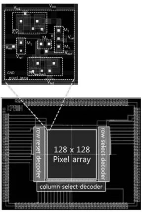
The prototype image sensor chip is composed of a 128 ø 128 array using the proposed APS, a row reset decoder, a row select decoder, and a column decoder. Fig. 8 shows the layout of the prototype image sensor chip. The prototype
Fig. 5. Simulation results of the variation of the output voltage with the PD gate voltage in the pseudo 3-transistor APS and the proposed APS.
Fig. 6. Measurement results of the variation of the output voltage with the light intensity in the pseudo 3-transistor APS and proposed APS.
Fig. 7. Measurement results of the variation of the output voltage with light intensity, as a function of the operation mode.
Table 1. Performance of the proposed pixel structure
Process Supply Voltage
Pixel size Photodetector type
Fill factor Dynamic range
0.35-Ïm 2P4M standard CMOS process 3.3 V
13.6 ø13.6 Ïm2
gate/body-tied PMOSFET type photodetector 14%
normal mode : 28 dB, WDR mode : 98 dB Proposed APS
image sensor chip was designed and fabricated using a 0.35- Ï m 2-poly 4-metal standard complementary metal oxide semiconductor (CMOS) process.
Fig. 9 shows a photograph of the imaging system board and block diagram. The imaging system is composed of the prototype image sensor chip, the bias circuits to adjust the image, an analog to digital converter (ADC), a field programmable gate aray (FPGA), and a local area network (LAN) port. The FPGA plays a role as a microcontroller unit. It governs the control switches, the row reset decoder, the row select decoder, and the column decoder in the image chip. The ADC is also controlled by the FPGA according to its datasheet. The LAN port can be connected to a LAN module to communicate via TCP/IP. Fig. 10 shows the output images of the system. Since the Ethernet module has an original internet protocol address, when we input the IP address into our PC, the communication using TCP/IP makes it possible to view the captured image.
Fig. 11 shows the output image of the imaging system as a function of the operation mode. The normal mode image had saturated parts in high illumination, but the WDR mode image was not saturated. This was similar to the measured results shown in Fig. 7. This means that the dynamic range was controlled by the operation mode.
4. CONCLUSIONS
A new approach for dynamic range extension using an additional gate/body-tied PMOSFET-type photodetector and an NMOSFET based on the pseudo 3-transistor APS has been proposed. We have presented a new pixel that can be switched between two operating modes depending on the transfer gate voltage: normal mode and WDR mode.
The proposed pixel was designed and fabricated using a 0.35- Ï m 2-poly 4-metal standard CMOS process.
Although the proposed pixel size increased in comparison
Fig. 8. Layout of the prototype image sensor chip.
Fig. 9. Imaging system; (a) photograph of the system board, (b) block diagram.
(b) (a)
Fig. 10. Output images of the imaging system.
Fig. 11. Output images of the imaging system, as a function of the operation mode; (a) normal mode, (b) WDR mode.
(a) (b)