• 검색 결과가 없습니다.

Extension of the Dynamic Range using the Switching Operation of In-Pixel Inverter in Complementary Metal Oxide Semiconductor Image Sensors

N/A
N/A
Protected

Academic year: 2021

Share "Extension of the Dynamic Range using the Switching Operation of In-Pixel Inverter in Complementary Metal Oxide Semiconductor Image Sensors"

Copied!
5
0
0

로드 중.... (전체 텍스트 보기)

전체 글

(1)

http://dx.doi.org/10.5369/JSST.2019.28.2.71 pISSN 1225-5475/eISSN 2093-7563

Extension of the Dynamic Range using the Switching Operation of In-Pixel Inverter in Complementary Metal Oxide Semiconductor Image Sensors

Donghyun Seong, Byoung-Soo Choi, Sang-Hwan Kim, Jimin Lee, Jewon Lee, Junwoo Lee, and Jang-Kyoo Shin

+

Abstract

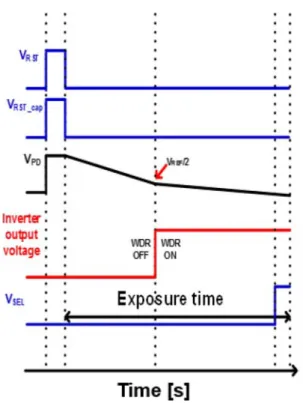
This paper proposes the extension of the dynamic range in complementary metal oxide semiconductor (CMOS) image sensors (CIS) using switching operation of in-pixel inverter. A CMOS inverter is integrated in each unit pixel of the proposed CIS for switching oper- ations. The n+/p-substrate photodiode junction capacitances are added to each unit pixel. When the output voltage of the photodiode is less than half of the power supply voltage of the CMOS inverter, the output voltage of the CMOS inverter changes from 0 V to the power supply voltage. Hence, the output voltage of the CMOS inverter is adjusted by changing the supply voltage of the CMOS inverter.

Thus, the switching point is adjusted according to light intensity when the supply voltage of the CMOS inverter changes. Switching operations are then performed because the CMOS inverter is integrated with in each unit pixel. The proposed CIS is composed of a pixel array, multiplexers, shift registers, and biasing circuits. The size of the proposed pixel is 10 µm × 10 µm. The number of pixels is 150 (H) × 220 (V). The proposed CIS was fabricated using a 0.18 µm 1-poly 6-metal CMOS standard process and its characteristics were experimentally analyzed.

Keywords: CMOS image sensor, Dynamic range extension, CMOS inverter, Switching operation, Sensitivity, Junction capac- itance

1. INTRODUCTION

Complementary metal oxide semiconductor (CMOS) image sensors (CIS) are used for camera applications, such as security cameras, webcam, and camcorders. CIS have several advantages over charge-coupled device (CCD) image sensors, including low power consumption, low cost, and compatibility with standard CMOS technology [1-2]. CIS are evaluated by considering their characteristics such as dynamic range, resolution, and power consumption. In this paper, we propose a dynamic range extension of CIS using switching operation of in-pixel inverter. The dynamic range is defined as the ratio between the full-well capacity and the floor noise. To extend the dynamic range of CIS, several techniques have been proposed [3-9]. Although they succeeded in achieving wide dynamic range, these techniques

have their disadvantages as well. For example, a CIS having characteristics of linear-logarithmic response was proposed [3].

The logarithmic active pixel sensor (APS) has excessive dynamic range. However, in logarithmic APS, fixed pattern noise (FPN) is a major problem because FPN is generated due to hot-carrier- induced threshold voltage shift in the logarithmic APS.

Additionally, the multiple sampling technique was proposed [4].

The multiple sampling technique also achieves a wide dynamic range by synthesizing different exposure time images.

However, a fast-moving object captured as an image is subject to image distortion. In a previous work, wide dynamic range CIS with adjustable sensitivity using a cascade metal-oxide semiconductor field-effect transistor (MOSFET) and an inverter was proposed [5]. The logarithmic response was used to extend the dynamic range using in-pixel inverter. In this research, it was observed that dynamic range extension is achieved by linearly changing the sensitivity of the pixel unit. The characteristics of the proposed CIS were evaluated using measurements. Thus, a dynamic range extension using a CMOS inverter in the unit pixel is proposed. According to the intensity of light incident on the proposed APS, it is possible to verify whether the CMOS inverter is in operation. When the CMOS inverter is turned on, the dynamic range of the proposed CIS is extended. On the other hand, when the CMOS inverter is off, the proposed CIS is School of Electronics Engineering, Kyunpook National University, 80

Daehakro, Bukgu, Daegu 41566, Korea

+

Corresponding author: [email protected]

(Received : Dec. 27, 2018, Revised : Jan. 11, 2019, Accepted : Jan. 18, 2019)

This is an Open Access article distributed under the terms of the Creative Commons Attribution Non-Commercial License(http://creativecommons.org/

licenses/bync/3.0) which permits unrestricted non-commercial use, distribution,

and reproduction in any medium, provided the original work is properly cited.

(2)

operated in the conventional mode as switching operation is not performed.

2. DESIGN AND OPERATING PRINCIPLE

2.1 Design of unit pixel

In this research, the dynamic range extension of CIS via the switching operation of in-pixel inverter using CMOS inverter, which is integrated in each pixel unit, is presented. The proposed unit pixel is based on the photodiode-type APS [10]. Fig. 1 shows the schematic diagram of the proposed unit pixel. The CMOS inverter (M6, M7), additional reset transistor (M1), switch transistor (M5), and n+/p-substrate (n+/p-sub) junction capacitances are included along with the unit pixel. In the proposed CIS, Node A in Fig. 1 shows the input node of the CMOS inverter which is equal to the input node of the source follower (M3). Node B shows the output node of the CMOS inverter connected to the gate of the M5 transistor. Two reset transistors (M1, M2) are used for the reset operation to deplete the electrons accumulated at the n+/p-sub junction. Finally, the selected transistor M4 is used to estimate the pixel output voltage V

OUT

.

In Fig. 2, the cross-sectional view of the proposed unit pixel is shown. It was proved previously that signal electrons are generated when the reverse-biased n+/p-sub junction photodiode is exposed to light [11]. On the other hand, a metal layer located on the upper side of the junction capacitance blocks the light, hence avoiding the exposure of the n+/p-sub junction capacitance. The n+/p-sub

junction capacitances are included for storing the signal electrons rather than generating them. Polycrystalline silicon (poly-Si) gates separate the light-receiving and electron-storage areas which comprise the n+/p-sub junction. The input gate of the CMOS inverter is connected to the n+ region of the light-receiving area.

The output node of the CMOS inverter is connected to the poly-Si gates to apply the switching operation according to light intensity.

2.2 Operating principle

To operate the proposed CIS, additional reset operations are used to deplete the electrons stored in the additional n+/p-sub capacitances. These additional reset operations haves to be added to the operation of conventional 3-Tr APS. In the schematic of the APS described in Fig. 1, the additional reset transistor (M1) can set the value of voltage for the initial condition before the exposure time. When the signal voltage at the n+ region of the photodiode is changed, the output voltage of the CMOS inverter changes from 0 V to V

REF

based on the V

REF

/2 voltage. Subsequently, the n+/p- sub junction capacitances are connected to the n+/p-sub photodiodes. Thus, the capacitance of the n+/p-sub photodiode increases and the sensitivity of the proposed pixel decreases. V

REF

of the M6 transistor is the supply voltage of the CMOS inverter, which can be adjusted to change the switching point.

In Fig. 3, the timing diagram of the proposed method for dynamic range extension is shown. First, reset operations are preformed to eliminate the signal electrons in the n+/p-sub junction. Subsequently, the signal voltage changes when signal electrons are generated at the n+/p-sub photodiode due to exposure to light. During the exposure time, when the input Fig. 1. Schematic diagram of the proposed unit pixel.

Fig. 2. Cross-sectional view of the proposed unit pixel.

(3)

voltage of the CMOS inverter is below V

REF

/2, the output voltage of the CMOS inverter changes from 0 V to V

REF

[12]. When the CMOS inverter is turned on, the switching operation is complete and the sensitivity of the unit pixel decreases since the n+/p-sub junction capacitances are connected to the n+/p-sub photodiode.

Finally, dynamic range extension is performed by the switching operation of the CMOS inverters located in each unit pixel.

Hence, the dynamic range extension is automatically performed at each unit pixel using the CMOS inverter.

3. RESULTS AND DISCUSSIONS

3.1 Measurement results

Several measurements were performed to verify the dynamic range extension of CIS using the switching operation of in-pixel inverter. Fig. 4 shows, the comparison of the pixel output voltage characteristics as a function of the light intensity in the conventional and WDR modes. When V

REF

is 0 V, the CMOS inverter is turned off during the exposure since the supply voltage is not applied to the CMOS inverter. On the other hand, when V

REF

is applied to the supply voltage of the CMOS inverter, the switching operation is performed in accordance with the light intensity. After the switching operation, the switch is turned by the output voltage of the CMOS inverter, causing the switch in each unit pixel to turn on.

Subsequently, additional capacitances are attached to the photodiode to decrease the sensitivity of the unit pixel. Fig. 4 shows that the switching operation is performed at around 1,000 lux light exposure and the dynamic range is extended.

Fig. 5 shows, the pixel output voltage characteristics as a function of the supply voltage of the CMOS inverter. Changing the supply voltage of the CMOS inverter changes, the switching point. In other words, the switching point is adjusted by changing the V

REF

voltage. When V

REF

is 0 V, the sensitivity is unchanged as the CMOS inverter is turned off and the additional capacitances are not connected to the n+/p-sub photodiode. In contrast, when V

REF

is 1.8 V, 2.7 V, or 3.3 V, the switching point is adjusted individually as the CMOS inverter is turned on at different times.

Fig. 3. Timing diagram for the operation of the proposed method of dynamic range extension.

Fig. 4. Comparison of pixel output voltage characteristics as a func- tion of the light intensity between the conventional mode and the wide dynamic range mode.

Fig. 5. Pixel output voltage characteristics according to power supply

voltage of in-pixel CMOS inverter.

(4)

Table 1 shows the characteristics of the proposed CIS, which was fabricated by the 1-poly 6-metal 0.18 µm standard CMOS process. The supply voltage is 3.3 V for analog circuits and 1.8 V for digital circuits. The resolution is 150 (H) × 220 (V) with a 100 µm

2

unit pixel pitch. The fill factor is 20.9 %. The dynamic range of the WDR mode operation is extended by 4 dB more than that of the conventional mode operation using the switching operation of the CMOS inverter..

Fig. 6 shows the captured images for different values of V

REF

supply voltage of the CMOS inverter integrated at each unit pixel.

When V

REF

is 0 V, the image of objects located in the front is saturated when the light intensity is high. On the other hand, when the V

REF

is changed to 3.3 V, the dynamic range is extended owing to the switching operation of the in-pixel CMOS inverter.

Comparing the images in Fig. 6 (a) and (b), it is evident that using the CMOS inverter extends the dynamic range.

3.2 Discussions

In the proposed CIS, the CMOS inverter is integrated in each unit pixel. The fill factor of the unit pixel decreases because additional transistors, such as the CMOS inverter, are integrated in

each unit pixel. To increase the fill factor of the unit pixel, the size of the transistors in the CMOS inverter needs to be optimized. In other words, when the minimum length of the MOSFET gate shortens, the size of transistors in a CMOS inverter can be minimized.

It is evident that the automatic operation to change the sensitivity during the exposure time can be used for WDR operation. The proposed CIS has the advantage of an automatic wide dynamic range operation based on light intensity. The WDR operation is performed according to the light intensity using the proposed unit pixel structure without changing the readout circuits. In the unit pixel, the additional n+/p-sub junction capacitance is included, whose value can be applied differently.

When this value increases, the sensitivity decreases after the switching operation.

Fig. 7 shows the results of the simulation of pixel output voltage characteristics according to the value of the n+/p-sub junction capacitance. The value of the n+/p-sub junction capacitance in each pixel are 10 fF, 30 fF, 50 fF, 70 fF, and 90 fF. Post the switching operation, the sensitivity of the unit pixel is dependent on the value of n+/p-sub junction capacitance.

4. CONCLUSIONS

Extension of the dynamic range using the switching operation of in-pixel inverter in CIS has been presented. The proposed CIS consists of a pixel array, multiplexers, shift registers, and biasing circuits. It is possible that the WDR mode or conventional mode is operated using the switching operation of in-pixel inverter according to the light intensity. The proposed CIS was fabricated using the 0.18 µm 1-poly 6-metal CMOS standard process.

Table 1. Characteristics of the proposed CMOS image sensor.

Parameter Value

Technology 1-poly 6-metal 0.18 µm CMOS process

Resolution 150 (H) × 220 (V)

Power supply Analog : 3.3 V, Digital : 1.8 V

Pixel pitch 10 µm × 10 µm

Dynamic range Conventional mode : approximately 25 dB WDR mode : approximately 29 dB

Fig. 6. Captured images when V

REF

is (a) 0 V, and (b) 3.3 V.

Fig. 7. Simulation results of pixel output voltage characteristics

according to the value of n+/p-sub junction capacitance.

(5)

Experiments were carried out to evaluate the characteristics of the proposed CIS. When the output of the CMOS inverter changes from 0 V to V

REF

, the sensitivity of the proposed pixel decreases as compared to the sensitivity of the unit pixel in the conventional mode. The in-pixel inverter was used to decrease the sensitivity of the unit pixel in the WDR mode of operation. As a result, the proposed CIS can be used for the dynamic range extension of CIS to acquire the images under various light conditions.

ACKNOWLEDGMENT

This work was supported by Integrated Circuit Design Education Center (IDEC) in Korea, the BK21 Plus project funded by the Ministry of Education, Korea (21A20131600011) and Samsung Electronics Co., Ltd.

REFERENCES

[1] M. Bigas, E. Cabruja, J. Forest, and J. Salvi, “Review of CMOS image sensors”, Microelectron. J., Vol. 37, No. 2, pp. 433-451, 2006.

[2] E. Fossum, “CMOS image sensors: Electronic camera on a chip”, IEEE Trans. Electron Devices, Vol. 44, No. 10, pp.

1689-1698, 1997.

[3] M. Bae, B.-S. Choi, S.-H. Jo, H.-H. Lee, P. Choi, and J.-K.

Shin, “A Linear-Logarithmic CMOS Image Sensor with Adjustable Dynamic Range”, IEEE Sens. J., Vol. 16, No.

13, pp. 5222-5226, 2016.

[4] J. Park, M. Mase, S. Kawahito, M. Sasaki, Y. Wakamori,

and Y. Ohta, “A 142dB Dynamic Range CMOS Image Sen- sor with Multiple Exposure Time Signals”, IEEE Asian Solid-State Circuits Conf., pp. 85-88, Hsinchu, Taiwan, 2005.

[5] D. Seong, B.-S. Choi, S.-H. Kim, J. Lee, and J.-K. Shin

“Wide Dynamic Range CMOS Image Sensor with Adjust- able Sensitivity Using Cascode MOSFET and Inverter”, J.

Sens. Sci. Technol., Vol. 27, No. 6, pp. 362-387, 2018.

[6] B. S. Choi, S. H. Jo, M. Bae, J. Kim, P. Choi, J. K. Shin and Y. Joo, “A Complementary Metal Oxide Semiconductor Image Sensor with Increased Dynamic Range Using Feed- back Reset Mechanism”, Sensor Letters, Vol.13, No. 8, pp.

658-662, 2015.

[7] K. Nishimura, Y. Sato, J. Hirase, R. Sakaida, M. Yanagida, T. Tamaki, M. Takase, H. Kanehara, M. Murakami, and Y.

Inoue, “An over 120dB simultaneous-capture wide- dynamic-range 1.6e− ultra-low-reset-noise organic-photo- conductive-film CMOS image sensor”, IEEE International Solid-State Circuits Conf., pp. 110-111, San Francisco, US, 2016.

[8] M. -W. Seo, T. Sawamoto, T. Akahori, T. Iida, T. Takasawa, K. Yasutomi and S. Kawahito, “A Low Noise Wide Dynamic Range CMOS Image Sensor With Low-Noise Transistors and 17b Column-Parallel ADCs”, IEEE Sens. J., pp. 2922-2929, 2013.

[9] J. -B. Chun, H. J. Jung, C. –M. Kyung, “Dynamic-Range Widening in a CMOS Image Sensor Through Exposure Control Over a Dual-Photodiode Pixel”, IEEE Trans. Elec- tron Devices, Vol. 56, No. 12, pp. 3000-3008, 2009.

[10] E. R. Fossum, “Active Pixel Sensors: Are CCD's Dino- saurs?”, Proc. of SPIE, pp. 2-14, CA, US, 1993.

[11] G. P. Weckler, “Operation of p-n Junction Photodetector s in a Photon Flux Integrating Mode”, IEEE J. Solid-State Cir- cuits, Vol. 2, No. 3, pp. 65-73, 1967.

[12] R. Jacob, CMOS Circuit Design, Layout, and Simulation,

Piscataway, IEEE Press, NJ, pp. 331-352, 1997.

수치

Fig. 2. Cross-sectional view of the proposed unit pixel.
Fig. 3. Timing diagram for the operation of the proposed method of dynamic range extension.
Fig. 6 shows the captured images for different values of V REF

참조

관련 문서

Modern Physics for Scientists and Engineers International Edition,

If both these adjustments are considered, the resulting approach is called a bootstrap-BC a -method (bias- corrected-accelerated). A description of this approach

③ A student who attended Korean course at KNU Korean Language Program and holds TOPIK Level 3 or a student who completed Korean course Level 4 at the KNU Korean Language

Five days later, on 15 January 1975, the Portuguese government signed an agreement with the MPLA, FNLA and UNITA providing for Angola to receive its independence on 11

· 50% exemption from tuition fee Ⅱ for the student with a TOPIK score of level 3 or higher or completion of level 4 or higher class of the Korean language program at the

Note (3) The Backlight inverter power must be turned on after the power supply for the logic and the interface signal is valid.. The Backlight inverter power must be turned

Since the digital input of a PLC has a high impedance, the digital output can also be connected to the PLC using the internal power supply of the inverter using terminal 6

그것은 이미지를 문자적 으로 서술하는 문제이며 옐름슬레브Hjelmslev[4]의 용어를 쓰자면 (코노테 이션과 반대되는 의미로서) 공정작용operation의