http://dx.doi.org/10.5369/JSST.2013.22.4.256 pISSN 1225-5475/eISSN 2093-7563
1. INTRODUCTION
Image sensor technology has progressed from advanced semiconductor technology. The complementary metal- oxide-semiconductor (CMOS) process offers the capability of integrating smart functions on imagers in a single chip [1-3]. As CMOS technology scales down, the pixel size is reduced for higher resolution sensors; thus, creating high- performance CMOS image sensors has become more difficult. A lower saturation level due to the small supply voltage and a higher noise level due to mismatch of the device cause the dynamic range to become a very significant problem [4-7].
The dynamic range of image sensors is defined as the ratio of the saturation signal level to the noise level. Natural scenes have a very wide range of illumination with light intensities varying over the 100 dB range or wider. To capture natural scenes with such a dynamic range, an
imager with wide dynamic range (WDR) is required.
However, the dynamic range of current commercial cameras without applying a special technique is limited to less than 60 dB. Various approaches have been developed to acquire WDR images [8-12]. Logarithmic sensors may extremely widen their dynamic range in the high- illumination region by compressing the image signal.
However, the conventional logarithmic technique that operates in the sub-threshold region suffers from low sensitivity at low light intensity. The quality of the output image of the logarithmic sensor is degraded by mismatches among the individual pixels in each sensor [13]. In the case of overflow integration, the capacitor method is inappropriate for small pixels because of their in-pixel lateral capacitor [14]. The multiple sampling technique provides WDR without pixel modifications. The major drawback of the conventional multiple sampling method is the requirement of additional frame memories and an image-synthesis process [15].
In this work, we propose a novel WDR CMOS active pixel sensor (APS) using a stacked photodiode structure based on a feedback mechanism without any complex circuit. The proposed sensor occupies less area and offers improved spectral response compared with that of the previous works [16, 17] owing to the stacked structure. The proposed technique for controlling the dynamic range
Extension of the Dynamic Range in the CMOS Active Pixel Sensor Using a Stacked Photodiode and Feedback Structure
Sung-Hyun Jo, Hee Ho Lee, Myunghan Bae, Minho Lee, Ju-Yeong Kim, Pyung Choi, and Jang-Kyoo Shin+
Abstract
This paper presents an extension of the dynamic range in a complementary metal-oxide-semiconductor (CMOS) active pixel sensor (APS) using a stacked photodiode and feedback structure. The proposed APS is composed of two additional MOSFETs and stacked P+/N-well/P-sub photodiodes as compared with a conventional APS. Using the proposed technique, the sensor can improve the spectral response and dynamic range. The spectral response is improved using an additional stacked P+/N-well photodiode, and the dynamic range is increased using the feedback structure. Although the size of the pixel is slightly larger than that of a conventional three-transistor APS, control of the dynamic range is much easier than that of the conventional methods using the feedback structure. The simulation and measurement results for the proposed APS demonstrate a wide dynamic range feature. The maximum dynamic range of the proposed sensor is greater than 103 dB. The designed circuit is fabricated by the 0.35-μm 2-poly 4-metal standard CMOS process, and its characteristics are evaluated.
Keywords : Feedback, Spectral response, Extension of dynamic range, Stacked photodiode
School of Electronics Engineering, Kyungpook National University, 1370 Sankyuk-dong, Buk-gu, Daegu 702-701, Korea
+Corresponding author: [email protected]
(Received : Jun. 13, 2013, Revised : Jul. 18, 2013, Accepted : Jul. 19, 2013) This is an Open Access article distributed under the terms of the Creative Commons Attribution Non-Commercial License(http://creativecommons.org/licenses/by- nc/3.0)which permits unrestricted non-commercial use, distribution, and reproduction in any medium, provided the original work is properly cited.
requires only two additional MOSFETs compared with the conventional three-transistor APS. The designed circuit is fabricated using 0.35
μm 2-poly 4-metal standard CMOS technology, and its characteristics are evaluated.
2. OPERATIONAL PRINCIPLE
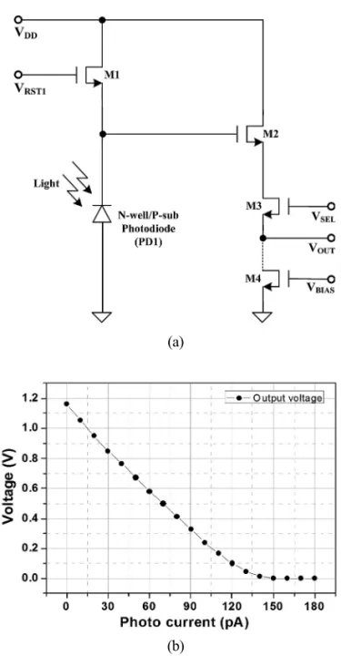
2.1 Conventional APSFig. 1(a) shows a conventional three-transistor APS with a simple structure and operating principle; it suffers from the problem of a narrow dynamic range. To overcome this
problem, a logarithmic pixel is proposed. This pixel consists of three transistors and a photodiode, similar to the conventional three-transistor APS. However, unlike the conventional three-transistor APS where the reset gate is controlled by a reset signal, the reset gate in the logarithmic pixel is connected to VDD and is generally operated in the sub-threshold region because the photocurrent is quite small.
2.2 Proposed APS
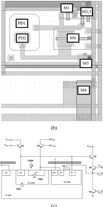
Fig. 2(a) shows the proposed APS, which consists of two additional MOSFETs and stacked P+/N-well/P-sub photodiodes, in comparison with the conventional APS;
Fig. 2(b) shows its layout. Because only two pn junctions (PD1 and PD2) are present in the same area, the spectral response of the proposed APS can be increased, which creates an effective depletion region that is even larger than the N-well/P-sub photodiode and leads to the highly absorbent blue wavelength compared with the N-well/P- sub photodiode [18]. The gate of M6 is connected to the output voltage, and the source and drain of M6 are connected to the floating diffusion node (FD) of the APS and the anode of PD2, respectively, as shown in Fig. 2(a).
This feedback structure allows significant extension of the dynamic range while maintaining high sensitivity under low illumination. Fig. 2(c) shows the cross section of the proposed APS.
Fig 1. Conventional APS. (a) Schematic and (b) Variation in the conventional three-transistor APS output voltage with photocurrent (simulation results).
(a)
(a)
(b)
Fig. 3 shows the operational sequence of the proposed APS. The sequence of operation is as follows. First, PD1 and PD2 are reset by M1, as shown in Fig. 3(a). At this time, feedback transistor M6 is in the sub-threshold region;
the source voltage of M6 is approximately 2 V, the gate voltage is 1.3 V, and the drain voltage is 2 V by inducing the reference voltage (V
REF). Photo-generated charges are simultaneously accumulated in both photodiodes after reset transistor M1 is turned off. Second, the output voltage of the proposed APS is decreased linearly until |V
OUT- V
REF| =
|V
threshold (M6)|, as shown in Fig. 3(b). Third, after a certain charge accumulation period, M6 is gradually turned on because of the decreased output voltage, which is connected to the gate of M6 (|V
OUT-V
REF| ≤ |V
threshold (M6)|).
During this time, the sensitivity slope decreases because of the feedback current of M6. As the incident light intensity
increases, the gate voltage of M6, which is connected to the output voltage, further decreases. Therefore, the output voltage is not saturated because more holes are induced in the channel of M6, and the source current in M6 increases, as shown in Fig. 3(d). This effect prevents the output voltage from saturating and thus increases the dynamic range of the APS.
3. RESULTS AND DISCUSSION
A photo-generated charge is created when the incident light hits the photodiodes (PD1 and PD2). Because the photodiode is reverse biased, the generated electrons and holes will be swept away from each other; the electrons will be swept to the cathode of the photodiode and the holes to the anode. Because this photocurrent is extremely small (from the femtoampere to the picoampere range), all charges generated by the photocurrent must be integrated during a period of time for it to be sensed by the gate of the readout transistor (M2).
The total capacitance of the proposed APS, namely, C
p, is equal to the sum of the photodiode capacitance and the capacitance at the gate of the readout transistor, i.e. C
pC
photodiode(PD1+PD2)+ C
gate(M2)+ C
source(M6).
Fig. 2. Proposed APS. (a) Schematic, (b) layout, and (c) cross- sectional view.
Fig. 3. Sequence of the operating principle of the proposed APS.
(a) Reset state, (b) Integration state, (c and d) Feedback state.
(b)
(c)
The proposed APS has a gate-controlled resistor (M6) to extend the dynamic range of the proposed APS. If the gate voltage exceeds the threshold voltage in the p-channel device, holes are induced in the underlying gate of M6.
Because this channel is connected to FD and the reference voltage node (V
REF), the structure electrically appears as an induced p-type resistor. As the gate voltage of M6, which is connected to the output node (V
OUT), decreases when the light intensity increases, more holes are induced in the channel, and its channel becomes more conducting. The feedback current of M6 gradually increases as the illumination level increases, as shown in Fig. 3(c).
Equation (1) shows the output voltage characteristic of the proposed APS. The voltage of FD (V
FD) is determined by the initial voltage (V
FD_RST1), photocurrents (I
PD1and I
PD2), and feedback current of M6:
where V
FD_RST1is the initial voltage of FD, V
GS(M6)is the gate voltage relative to the source voltage of the feedback transistor, and V
DS(M6)is the drain voltage relative to the source voltage of the feedback transistor.
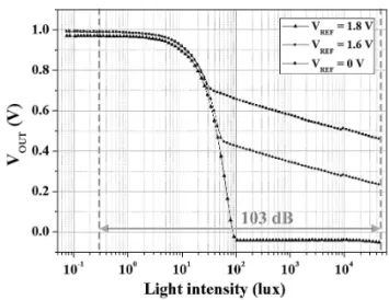
Fig. 4 shows the variation in the output voltage with the photocurrent when the integration time is 1 ms. In the case of the conventional APS, the output voltage is saturated at 160 pA, as shown in Fig. 1(b). Because of the output voltage feedback structure, the proposed APS is not saturated at 100 nA, as shown in Fig. 4. Fig. 5 shows the variation in the output voltage with the light intensity when the integration time is 1 ms. The dynamic range of the proposed APS is significantly extended to 103 dB. The proposed APS can not only improve the sensitivity at low illumination levels but also extend the dynamic range according to the feedback structure. Compared with previously reported WDR methods, the proposed method is very simple and powerful.
4. CONCLUSIONS
In this study, extension of the dynamic range of the CMOS APS using a stacked photodiode and feedback structure has been designed and fabricated. The dynamic range of the proposed APS is greater than 103 dB according to the feedback structure. Although the pixel size of the proposed APS is slightly larger than that of the conventional three-transistor APS owing to the two additional MOSFETs, dynamic range control is easier than that of the other reported WDR methods. In addition, the dynamic range of the proposed APS significantly increases while maintaining high sensitivity under low illumination because of the feedback structure. The proposed feedback
Fig. 4. Variation in the proposed APS output voltage with photocurrent when the integration time is 1 ms (simulation results).
(1)
Fig. 5. Variation in the proposed APS output voltage with light intensity when the integration time is 1 ms (measurement results).