저작자표시-비영리-변경금지 2.0 대한민국 이용자는 아래의 조건을 따르는 경우에 한하여 자유롭게
l 이 저작물을 복제, 배포, 전송, 전시, 공연 및 방송할 수 있습니다. 다음과 같은 조건을 따라야 합니다:
l 귀하는, 이 저작물의 재이용이나 배포의 경우, 이 저작물에 적용된 이용허락조건 을 명확하게 나타내어야 합니다.
l 저작권자로부터 별도의 허가를 받으면 이러한 조건들은 적용되지 않습니다.
저작권법에 따른 이용자의 권리는 위의 내용에 의하여 영향을 받지 않습니다. 이것은 이용허락규약(Legal Code)을 이해하기 쉽게 요약한 것입니다.
Disclaimer
저작자표시. 귀하는 원저작자를 표시하여야 합니다.
비영리. 귀하는 이 저작물을 영리 목적으로 이용할 수 없습니다.
변경금지. 귀하는 이 저작물을 개작, 변형 또는 가공할 수 없습니다.
Ph.D. Dissertation
Non-classical crystallization of Al 2 O 3 films by positively charged
nanoparticles during aerosol deposition
By Subin Lee
August 2022
Department of Materials Science and Engineering
College of Engineering
Seoul National University
Non-classical crystallization of Al 2 O 3 films by positively charged
nanoparticles during aerosol deposition
지도 교수 황 농 문
이 논문을 공학박사 학위논문으로 제출함
2022 년 8 월
서울대학교 대학원
재료공학부
이 수 빈
이수빈의 공학박사 학위논문을 인준함
2022 년 08 월
위 원 장 한 흥 남 (인)
부위원장 황 농 문 (인)
위 원 김 미 영 (인)
위 원 권 영 균 (인)
위 원 정 대 용 (인)
i
Abstract
Non-classical crystallization of Al 2 O 3 films by positively charged
nanoparticles during aerosol deposition
Subin Lee Department of Materials Science and Engineering College of Engineering The Graduate School Seoul National University
Thin film growth through non-classical crystallization with a building block of charged nanoparticles (CNPs) has been studied in several fields, including chemical vapor deposition (CVD) and physical vapor deposition (PVD). To determine whether the same mechanism can be applied for aerosol deposition (AD) at room temperature, the generation and deposition behavior of CNPs were studied in the AD process for the first time. By measuring the current and examining the bias effect on the deposition behavior, it was confirmed that the fragmentation of Al2O3 particles generated numerous positively charged secondary nanoparticles as well as electrons by fracto-emission. In this work, the secondary particles
ii
passing between the two parallel biased and grounded electrodes were captured by the TEM grid membrane on each electrode, and it was revealed that they were mainly positively charged. Neutral secondary nanoparticles, not deflected by the electric field, produced a porous film on the silicon substrate, whereas charged secondary nanoparticles produced a dense film. The excess positive charging effects on the stacking fault energies of main slip systems were examined by density functional theory (DFT) calculations. When the electrons were removed, the activation barriers to create the stacking fault were decreased. The hypothesis that positive charges induce plastic deformation of secondary particles was supported by experiments and ab initio calculations. These results suggest that the positively charged secondary particles may be a major flux for film growth in the AD process. Combining the results, an aerosol deposition mechanism considering the charging effect was proposed.
Keyword : Non-classical crystallization, aerosol deposition, nanoparticles, ceramics, plastic deformation
Student Number : 2017-22773
iii
Table of Contents
Abstract ... ⅰ
List of Figures ... ⅴ
List of Tables ... ⅷ
Chapter 1. Introduction... 1
1.1 Non-classical crystallization... 2
1.2 Aerosol deposition... 7
Chapter 2. Generation of electrons and positively charged secondary nanoparticles by fracto-emission...10
2.1 Introduction ... 11
2.2 Experimental method... 13
2.3 Results and discussion ... 17
2.4 Conclusion ... 36
Chapter 3. Deposition behavior of secondary nanoparticles with and without positive charge ...37
3.1 Introduction ... 38
3.2 Experimental method... 40
3.3 Results and discussion ... 43
3.4 Conclusion ... 53
iv
Chapter 4. Positive charge effect on plastic deformation of Al
2O
3(ab-initio calculation) ...54
4.1 Introduction ... 55
4.2 Computational method ... 56
4.3 Results and discussion ... 59
4.4 Conclusion ... 66
Chapter 5. Effect of discharge on optical and mechanical properties of Al
2O
3films ...67
5.1 Introduction ... 68
5.2 Experimental method... 70
5.3 Results and discussion ... 72
5.4 Conclusion ... 84
Chapter 6. Aerosol deposition mechanism of Al
2O
3films...85
Referernces ...92
Abstract in Korean...103
v
List of Figures
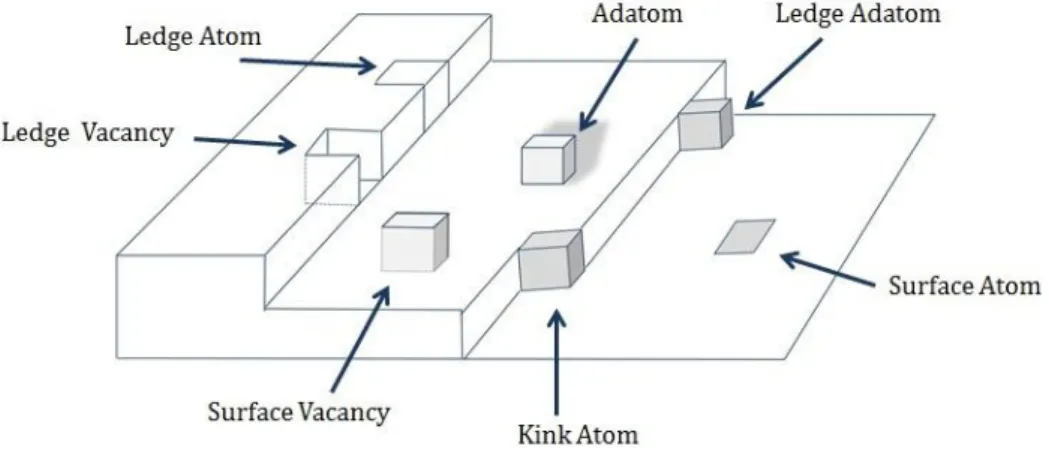
Figure 1.1 Terrace-Ledge-Kink model, which represents the growth by atom-atom attachment.
Figure 1.2 Schematic representation of classical and non-classical crystallization. (a) classical crystallization pathway, (b) oriented attachment of primary nanoparticles forming an iso-oriented crystal upon fusing, (c) mesocrystal formation via self-assembly of primary nanoparticles covered with organics. See text for details.
Figure 2.1 Schematic of AD reactor and apparatuses used to measure electric current between substrate 1 and ground and to apply DC bias to substrate 2.
Figure 2.2 (a) TEM image of original α-Al2O3 particles and (b) SAED pattern of original particle. Cross-sectional (c) FE-SEM and (d) bright-field TEM images of Al2O3film deposited by 10 scans on a sapphire substrate by AD and (e) high-magnification image of (d) with SAED pattern. (d) shows a magnified image of the lower-right square in (c), and (e) shows a magnified image of the upper-right square in (d).
Figure 2.3 Current density by (a) N2gas and (b) nonfractured Al2O3
particles.
Figure 2.4 Current density measured on substrate 1 with inset of dashed square indicating film surface current density.
vi
Figure 2.5 Film surface current density with varying (a) gas flow rates and (b) stand-off distances.
Figure 2.6 Al2O3 film deposited on Ti substrate according to film surface current density of (a) -19.66 nA/mm2, (b) -159.34 nA/mm2, and (c) -1466.18 nA/mm2.
Figure 2.7 Current density measured on substrate 2 during film deposition.
Figure 2.8 (a) Schematics of apparatuses used to capture secondary particles on membrane for TEM and to apply DC bias voltage. TEM images of Al2O3 secondary particles on membrane captured under applied bias voltages of (b) 0 V, (c) +300 V, and (d) -300 V.
Figure 3.1 Schematics of (a) the AD reactor and (b) apparatuses used to apply the DC bias to generate the electric field between the two electrodes and to deflect the track of secondary charged particles
Figure 3.2 TEM images of (a) an original Al2O3 particle with the inset indicating its SAED pattern, (b) secondary nanoparticles captured on the positive electrode, and (c) secondary nanoparticles captured on the grounded electrode
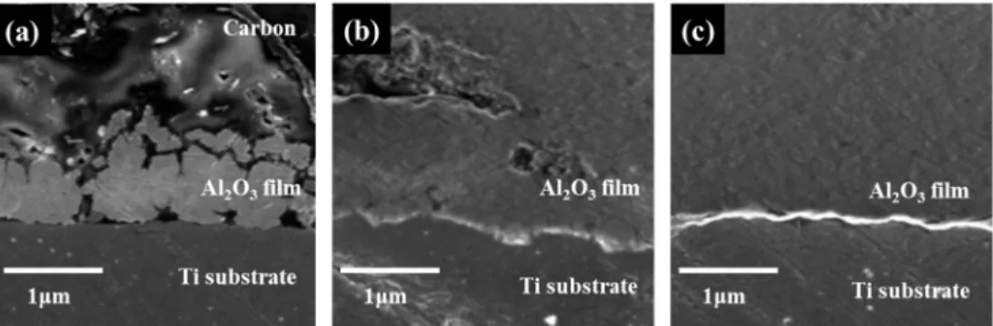
Figure 3.3 (a) Cross sectional TEM image of the Al2O3film deposited on the substrate 2 under the condition where the bias was not applied to the electrode, (b) high magnification bright field TEM image of the
vii
film in (a) with a dark single grain indicated in the dashed circle, (c) SAED pattern of the film, and (d) current measured at the substrate 2 during deposition
Figure 3.4 (a) Cross sectional TEM image of the Al2O3film deposited on the substrate 2 under the condition where the bias of + 250 V was applied to the electrode, (b) high magnification bright field TEM image of (a) with a dark single grain indicated in a dashed circle, (c) SAED pattern of the film, and (d) current measured at the substrate 2 during deposition
Figure 4.1 Sequential changes in structure during slip along (a) basal, (b) pyramidal, (c) asymmetric prismatic, and (d) symmetric prismatic planes, where yellow and blue spheres represent oxygen and aluminum atoms, respectively, and black dashed line represents slip plane.
Figure 4.2 Variation of GSF energy with displacement along (a) basal, (b) pyramidal, (c) asymmetric prismatic, and (d) symmetric prismatic planes during slip with respect to charging.
Figure 5.1 Schematic of AD reactor and apparatuses used to measure electric current between substrate 1 and ground and optical emission.
Figure 5.2 Al2O3films deposited in various gas atmospheres.
Figure 5.3 Current density measured on substrate when N2 gas was
viii used as carrier gas.
Figure 5.4 Current density measured on substrate when He gas was used as carrier gas.
Figure 5.5 Optical spectra measured by spectrometer when (a) N2
and(b) He gas was used as carrier gas.
Figure 5.6 Hardness of Al2O3 films according to gas flow rate when (a) N2and(b) He gas was used as carrier gas.
Figure 5.7 Al2O3 films deposited on insulating (a) glass, (b)quartz, and (c) alumina substrates and on conducting (d) ITO, (e) FTO, (f) Fe, (g) W, (h) Cu, and (i) Ti substrates.
Figure 6.1 Aerosol deposition mechanism.
List of Tables
Table 2.1 Film surface current density with varying gas flow rates and stand-off distances.
1
Chapter 1. Introduction
2
Chapter 1. Introduction
1.1 Non-classical Crystallization
The classical crystallization growth model begins with primary building blocks such as atoms, ions, or molecules and forms clusters based on the interaction of surface and crystal lattice energies. The core of classical crystallization is nucleation and growth, which can be easily understood as a homo nucleation phenomenon occurring in a solution. There is a certain solute solubility for each solvent, and any excess solute will result in precipitation and the formation of nanocrystals. Some clusters eventually grow to the size of a critical crystal nucleus, and these primary nanoparticles continue to grow via atom-by-ion attachment and unit cell replication.
The incorporation of one atom in this method is determined by the surface state of the cluster when it reaches critical size[1]. When atoms attach to the surface and produce excess energy, they are not incorporated and are eventually annihilated; however, if they do not produce excess energy for the overall system, they are incorporated and grow. This is the basic idea behind the TLK model, which is depicted in Fig. 1.1, and is widely accepted as the mechanism for the formation of nanostructures such as particles and thin films[2]. When an adatom sits on a terrace with a smooth interface, it diffuses
3
through the ledge and eventually enters the crystal through the kink.
This behavior is caused by the different surface energies of the crystal faces. Crystal faces with high surface energies grow the fastest and are minimized or even eliminated in the final morphology as shown in Fig. 1.2(a).
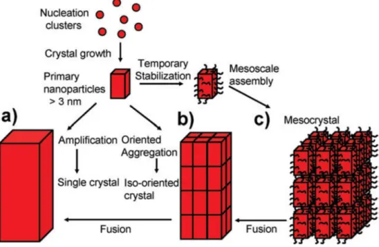
However, evidence indicating that crystals grow by the building block of nanoparticles have been reported recently. The formation of crystals by the building blocks of nanoparticles is known as non- classical crystallization, and it has been extensively studied over the last decade[3-9]. This new concept differs significantly from the classical understanding of crystal growth. Non-classical crystallization, in contrast to the classical crystallization, is particle- mediated and involves a mesoscopic transformation process[10]. Fig.
1.2(b) summarizes the main pathways of non-classical crystallization. Primary nanoparticles are orientedly attached to form iso-oriented crystals, which can fuse together to form a single crystal. If the nanoparticles are coated with organic components, they can assemble to form a mesocrystal as shown in Fig. 1.2(c).
Non-classical crystallization can also be applied in gas phase synthesis of thin films and nanostructures using chemical vapor deposition (CVD) and physical vapor deposition (PVD). Hwang et al.
published more than 100 SCI papers on non-classical crystallization
4
in the thin film deposition process.[11-14]
5
Figure 1.1 Terrace-Ledge-Kink model, which represents the growth by atom-atom attachment.
6
Figure 1.2 Schematic representation of classical and non-classical crystallization. (a) classical crystallization pathway, (b) oriented attachment of primary nanoparticles forming an iso-oriented crystal upon fusing, (c) mesocrystal formation via self-assembly of primary nanoparticles covered with organics. See text for details. [15]
7
1.2 Aerosol Deposition
Aerosol deposition (AD) is a method of depositing films by spraying ceramic particles at room temperature[16]. Since a dense film can be formed by AD at room temperature, AD has been used in many applications, such as solid oxide fuel cells (SOFCs)[17], hydroxyapatite (HA) coatings[18, 19], flexible dye-sensitized solar cells[20], and piezoelectric materials[21]. The mechanism by which the dense film forms at room temperature by AD is currently not clearly understood, and it has been phenomenally summarized as room temperature impact consolidation (RTIC)[22].
The phenomenological features of film formation by AD can be described as follows. First, the raw materials are seriously limited to brittle ceramic materials. Ductile metals are not appropriate for AD, as they do not easily form bonds with the substrate[23], although the deposition of some metallic materials has been reported as an exception[24, 25]. Second, aerosol particles need a critical speed ranging from subsonic to supersonic for successful deposition. The speed depends on the mechanical properties of feedstock materials and substrates. The critical velocity for AD of alpha-alumina was reported to be ~ 150 m/s, and that for lead zirconia titanite (PZT) was reported to be ~ 100 m/s[26]. Notably,
8
these velocities are considerably lower than those required for other coating methods using collision of solid particles in the absence of thermal energy assistance. For example, the thermal spray coating method involves melting a powder at a temperature of several thousand degrees for deposition and requires a particle velocity of ~ 1000 m/s[27]. The cold spray coating method used for metal and cermet does not require powder melting but requires heating the carrier gas to several hundred degrees and a high particle speed of 500–1500 m/s[28]. Third, the ceramic particles collide with the substrate, causing fragmentation and deposition within a very short time. Crystallite size reduction has been observed due to the fracture and plastic deformation of ceramic particles. For example, submicron-sized single-crystal Al2O3
particles produced a dense film having a nanocrystalline structure with a crystallite size of 10 nm[29]. Last, the increase in local temperature and pressure due to the impact of ceramic particles is very low compared to those of other ceramic fabrication methods.
According to a finite-element method (FEM) simulation, particle melting did not occur during the deposition process. The increase in the local temperature of 0.3 μm-sized Al2O3particles colliding with the substrate at a speed of 300 m/s did not exceed 600 K, and the shock pressure upon impact did not exceed 4 GPa[26]. These
9
values are far below the requirements for bulk ceramic fabrication with conventional sintering or shock compaction methods. Recent molecular dynamics (MD) simulation results for AD of ceramic materials such as nanoscale TiO2[30], HA[31], and yttria- stabilized zirconia (YSZ)[32] have reported that the temperature during particle collision can rise to 1200-1300K and the pressure up to 20 GPa at high impact velocity. It is reported that plastic deformation of ceramic particles may occur at such high temperatures and pressures.
10
Chapter 2. Generation of electrons and positively charged secondary
nanoparticles by fracto-emission
11
Chapter 2. Generation of electrons and positively charged secondary nanoparticles by
fracto-emission
2.1 Introduction
Since the early stage of AD research, many studies have focused on the role of the kinetic energy of ceramic particles flying at a high velocity to elucidate the mechanism[29, 33]. However, since the velocity of particles in AD is very low compared to other processes that use particle collisions, no satisfactory explanation has been found. A new perspective of crystallization in which crystals grow by the building block of nanoparticles, called nonclassical crystallization has been intensively studied recently [34, 35]. Most studies on nonclassical crystallization have been conducted in solution, but Hwang et al.[36] studied the film growth by nanoparticles via chemical vapor deposition (CVD) and some physical vapor deposition (PVD) processes. They suggested that the charge carried by the nanoparticles plays a critical role in the evolution of dense films because it makes the nanoparticles superplastic or liquid-like. In particular, in Section ‘ 14.2.8
12
Aerosol Deposition’ in [36], an effort was made to find evidence for the charging of particles during AD, and it cited Fuchita et al.’s work[37], where the static electricity induced by the friction between powder particles was mentioned based on the observation of luminescence during AD. It was further noted that the presence of charge will weaken the bond strength of at least the surface atoms of the particles and contribute to the evolution of the dense films and that it is difficult to imagine the evolution of such dense fi lms from the impact of neutral nanoparticles.
Motivated by this background, we study the possibility of generating charges during the AD process. If an appreciable number of charges is shown to be generated by the current measurement, it is highly probable that the nanoparticles may be charged. If the nanoparticles become charged, the AD mechanism could be explained by the non-classical crystallization of thin films based on the theory of charged nanoparticles (CNPs)[36]. In relation to this direction of research, the electron emission during AD was reported[38], and Fuchita et al.[39] noted that positively charged powder and fractoelectrons may play an important role in ceramic sintering during AD. Here, the generation of electric charges during the AD process was measured by the current, and
13
the role of these charges in the evolution of dense films was elucidated.
2.2 Experimental method
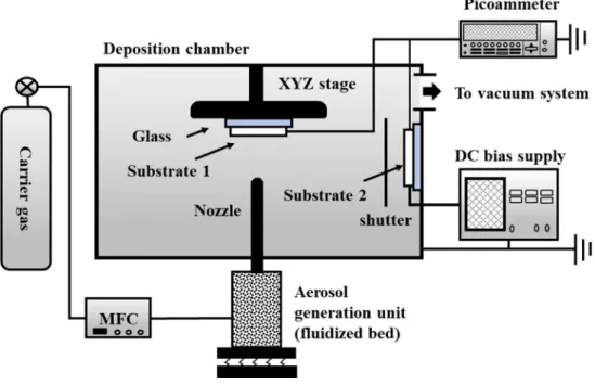
A schematic of the AD reactor used in this experiment is shown in Fig. 2.1. N2 as the carrier gas was passed through the vibrating aerosol generation unit carrying a fine ceramic powder. The particle- laden flow was accelerated through the converging type nozzle with orifice and inlet sizes of 5 x 1 mm2and 10 x 8 mm2, respectively, and collided with substrate 1 connected to the stage, forming a dense film.
Single-crystal α-Al2O3 powder with an average size of 0.5 μm was used as a feedstock material. The velocity of the particle was controlled by the flow rate of the N2 carrier gas, which was varied from 1 to 9 liters per min (LPM). During the process, the pressure inside the deposition chamber was kept below 1 Torr, and the stand- off distance between the nozzle orifice and substrate 1 was controlled within 1–20 mm.
To confirm the generation of electric charges by fracto-emission during and after the fracture of original particles, a picoammeter was installed to measure the current in real time between substrate 1 and the ground, as shown in the upper-right part of Fig. 2.1. The original
14
particles were fractured into numerous nanoparticles during their collisions with the substrate 1. To examine the current by non- fractured Al2O3 particles carried by the N2 gas, we used a Faraday cup that was placed outside the deposition chamber just above the aerosol generation unit. In this way, the current was measured before the Al2O3particle-laden N2carrier passed through the nozzle. Since the Al2O3 particle-laden N2 carrier gas did not pass through the nozzle, the velocity was not high, and therefore the aerosol Al2O3
particles did not fracture. Thus, the charges carried by nonfractured aerosol Al2O3particles could be measured on the Faraday cup.
After the original particles were fractured into nanoparticles during collision with substrate 1, some fractured nanoparticles bounced from substrate 1 to substrate 2, forming a dense film. To determine whether these bouncing nanoparticles (hereafter, secondary particles) carried charges, the current was also measured on substrate 2. The center of substrate 2 was ~ 250 mm away from the center of substrate 1 in the horizontal direction. The two centers coincided in the vertical direction, although that of substrate 2 appeared lower than that of substrate 1 in Fig. 2.1. Note that the substrate size of 10 mm × 10 mm × 1 mm was much smaller than the chamber size of 500 mm × 500 mm × 500 mm. If the secondary particles carried charges, their deposition and capturing
15
behavior would be affected by the electric bias. To evaluate this possibility, a DC bias voltage of + 300 V or – 300 V was applied between substrate 2 and the grounded chamber, as shown in the lower-right of Fig. 2.1. A shutter was installed above substrate 2 to control the time of deposition on substrate 2 or to capture the secondary nanoparticles on the membrane of the transmission electron microscopy (TEM) grid during the bias experiment. For film deposition, sapphire, silicon, and titanium were used as substrates 1 and 2, and the stage of substrate 1 was moved back and forth in the horizontal direction at a scanning speed of 1 mm/min. For the current measurement, titanium was used as substrates 1 and 2, and the stage of substrate 1 was fixed. Glass plates were placed between substrate 1 and the stage and between substrate 2 and the chamber wall to electrically float substrates 1 and 2 while measuring the current. The hardness of Al2O3films was measured by a nano-indentation system.
The cross-sections of the films and captured secondary particles were analyzed by field emission scanning electron microscopy (FE- SEM, SUPRA, Carl Zeiss) and high-resolution TEM (HRTEM, F20, Tecnai), respectively. Selected area electron diffraction (SAED) patterns were observed to examine the crystallinity of films and particles.
16
Figure 2.1 Schematic of AD reactor and apparatuses used to measure electric current between substrate 1 and ground and to apply DC bias to substrate 2.
17
2.3 Results and discussion
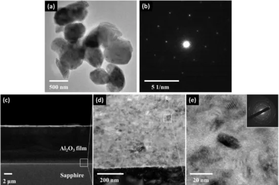
Fig. 2.2(a) shows a TEM image of the original α-Al2O3 particles used in this study. As stated by the manufacturer, the α-Al2O3
particles had an average size of ~500 nm. From the SAED pattern in Fig. 2.2(b), we can see that that the original particles are single crystals. Figs. 2.2(c), (d) and (e) show cross-sectional image of the Al2O3film deposited with 10 scans by AD. A dense Al2O3film with a thickness of several micrometers was formed on the sapphire substrate, as shown in Fig. 2.2(c). The hardness of the film measured by a nano-indentation system was 12.38 ± 0.5 GPa. The bright- field TEM images in Figs. 2.2(d) and (e) revealed that the as- deposited film had a nanocrystalline structure with a crystal size of 10–20 nm. Fig. 2.2 suggests that the 500 nm-sized particles collided with the substrate and then fractured into small-sized particles and plastically deformed to form a dense film.
18
Figure 2.2 (a) TEM image of original α-Al2O3 particles and (b) SAED pattern of original particle. Cross-sectional (c) FE-SEM and (d) bright-field TEM images of Al2O3film deposited by 10 scans on a sapphire substrate by AD and (e) high-magnification image of (d) with SAED pattern. (d) shows a magnified image of the lower-right square in (c), and (e) shows a magnified image of the upper-right square in (d).
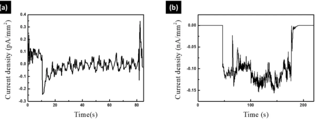
19 2.3.1 Current by fracto-emission
Fig. 2.3(a) shows the current measured on substrate 1 under the flow of a particle-free N2 carrier gas. The flow rate of the carrier gas was 7 LPM, which is high enough to form a dense film when particles flow together. As shown in Fig. 2.3(a), the current was negative, which appeared to be caused by the carrier gas. The current fluctuated when the gas flow was turned on and off. Before the gas flow, the current was negligibly small being close to zero.
However, after the gas flow, an appreciable amount of negative current was measured although it was less than -0.1 pA/mm2.
To examine how the current was changed when the Al2O3particles were carried by the N2 gas, a Faraday cup was placed outside the deposition chamber just above the aerosol generation unit. In this way, the current was measured before the Al2O3 particle-laden N2
carrier passed through the nozzle. Since the Al2O3particle-laden N2
carrier gas did not pass through the nozzle, the velocity was not high, and therefore the aerosol Al2O3 particles did not fracture. Thus, the charges carried by nonfractured aerosol Al2O3 particles could be measured on the Faraday cup, as shown in Fig. 2.3(b). The measured negative current was increased abruptly and ranged from -0.1 to - 0.15 nA/mm2. As seen by comparing Fig. 2.3(a) with Fig. 2.3(b), the current measured with the particle-laden flow was three orders of
20
magnitude higher than that measured with the particle-free gas flow.
Since such electric charges generated by the particle-laden flow were attributed to triboelectricity, which came from collisions between particles or between particles and the aerosol generation unit, they cannot be avoided in the process of supplying original particles.
When a film is deposited on a substrate via AD, aerosol Al2O3
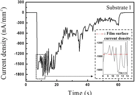
particles collide on the substrate at a speed of ~ 150 m/s and fracture into numerous nanoparticles on the substrate [26]. During the fracture of original particles, fracto-emission, by which electrons, ions, or photons are emitted, occurs[40], generating electrons. To measure the number of charges generated during AD, we measured the current on substrate 1. Fig. 2.4 shows the results, where the solid line represents the currents measured on substrate 1. As in the previous current measurements, the gas flow rate was 7 LPM, and a dense film was formed on the titanium substrate under this condition.
At the beginning of the deposition, an extremely high negative current of -1.5 μA/mm2 was measured on substrate 1. This value is more than four orders of magnitude higher than the previous current measured with the nonfractured Al2O3particles in Fig. 2.3(b).
Fig. 2.4 shows that many negative charges are generated during the fracture of original particles upon impact on the substrate. Fig. 2.4
21
shows that the amount of the measured negative current on the substrate 1 decreased as the deposition time increased from 20 s to 40 s and then to 60 s because the conducting titanium metal surface was coated by an insulating Al2O3film. Because of the insulating Al2O3
surface layer, the actual number of charges generated by the fracturing of particles could not be properly measured. After 60 s, the supply of aerosol Al2O3 particles was stopped, and the current returned to the original value before AD, as shown in Fig. 2.4. To compare the number of charges generated under different AD conditions, the film surface current density was defined as the average of the measured current density over the first 5 s after the flow of the original particles was turned on. As shown in the dashed square in Fig. 2.4, the flow was turned on at ~ 8 s, and the film surface current density was the average current measured between 8 and 13 s.
22
Figure 2.3 Current density by (a) N2gas and (b) nonfractured Al2O3
particles.
23
Figure 2.4 Current density measured on substrate 1 with inset of dashed square indicating film surface current density.
24
2.3.2 Relationship between film surface current density and film density
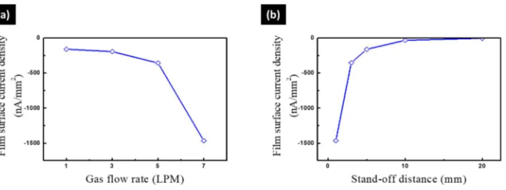
The processing condition would affect the current generation, which would affect the deposition behavior of films. To examine these relations, the film surface current density was measured in terms of two processing parameters: the gas flow rate of the carrier gas and the stand-off distance between the nozzle and substrate 1. The particle velocity refers to the average velocity of particles during their flight from the nozzle to the substrate. When the stand-off distance was 5 mm, the particle velocities measured by the time-of- flight method[41] in which a part of the particles was screened using a slit and the unscreened part of particles deposited on a moving substrate, were 35, 75, 110, and 130 m/s at gas flow rates of 1, 3, 5, and 7 LPM, respectively. Due to the difficulty in placing the slit, the particle velocity could not be measured at a stand-off distance of 1 mm. Since the particles have resistance from the secondary particles or gas bounding from the substrate, their velocity decreases with distance. Therefore, as the stand-off distance is decreased, the impact velocity will increase, and vice versa.
In Fig. 2.5(a), the film surface current density is plotted with the gas flow rates of 1, 3, 5 and 7 LPM at a stand-off distance of 1 mm.
The negative current increased with the gas flow rate and reached a
25
maximum value at 7 LPM. In Fig. 2.5(b), the film surface current density is plotted with the stand-off distances of 1, 3, 5, 10 and 20 mm at a gas flow rate of 7 LPM. The negative current increased as the stand-off distance decreased and reached a maximum at 1 mm.
When the gas flow rate was increased from 1 to 3 LPM, the collision between the particles and the substrate did not lead to sufficient fracturing of the original particles. Since the amount of electron emission is proportional to the degree of particle fracture, the measured current density at the substrate would have increased with the gas flow rate. This was indicated by the relatively low film surface current density, which was lower than that when the gas flow rate was 5 and 7 LPM. When the stand-off distance was increased from 1 mm to 20 mm, the velocity of the original particles decreased, leading to insufficient fracturing of the original particles. Since the amount of electron emission is proportional to the degree of particle fracture, the measured current density at the substrate would have decreased as the stand-off distance increased. This was also indicated by the film surface current density, which decreased as the stand-off distance increased.
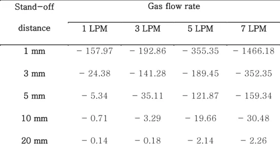
The numerical values of the film surface current measured with varying gas flow rates and stand-off distances are summarized in Table 1, clearly showing that the negative current increased as the
26
gas flow rate increased and the distance decreased, as shown in Fig.
2.5. Clearly, the current was accompanied by the fracture of original particles, confirming that the source of the current was electrons generated from fracto-emission. Fig. 2.5 and Table 2.1 indicate that the fracturing of original particles is enhanced by increasing the gas flow rate and decreasing the stand-off distance, both of which increase the velocity and thereby the impact energy of original particles.
The general observation is as follows. At the stand-off distance of 1 mm, when the gas flow rate was in the range of 1–3 LPM, a partially porous film was formed in some areas, and no film was formed in other areas. On the other hand, at the gas flow rates of 5 and 7 LPM, the film surface current density increased significantly, and a dense film was formed at the same stand-off distance. At the gas flow rate of 7 LPM, when the stand-off distance was 1 mm, a dense film was observed. Although the film surface current density at a stand-off distance of 3 mm decreased to one-third of that at a stand-off distance of 1 mm, a dense film was still formed at the same gas flow rate, 7 LPM. In the case of 5 mm, a partially porous film was formed, but when it exceeded 5 mm, no film was formed on the substrate, and the initial particles were embedded on the substrate at the gas flow rate of 7 LPM.
27
Therefore, the film density and the film quality depended strongly on the film surface current density. Representative cross-sectional FE-SEM images of the films formed at the three different film surface current densities are shown in Fig. 2.6. Fig. 2.6(a) shows a film of very poor quality with high porosity, which was deposited at a current density of -19.66 nA/mm2, a gas flow rate of 5 LPM and a stand-off distance of 10 mm. Similar film microstructures were observed when the measured film surface current density was less than -100 nA/mm2. Fig. 2.6(b) shows a film with less porosity deposited at a current density of -159.34 nA/mm2, a gas flow rate of 7 LPM and a distance of 5 mm. Similar film microstructures were observed when the measured film surface current density was between -100 nA/mm2and -300 nA/mm2. Fig. 2.6(c) shows a dense film with almost zero porosity deposited at a film surface current density of -1466.18 nA/mm2, a gas flow rate of 7 LPM and a distance of 1 mm. Similar film microstructures were observed when the current density was higher than -300 nA/mm2.
28
Figure 2.5 Film surface current density with varying (a) gas flow rates and (b) stand-off distances.
29
(unit: nA/mm2) Stand-off
distance
Gas flow rate
1 LPM 3 LPM 5 LPM 7 LPM
1 mm - 157.97 - 192.86 - 355.35 - 1466.18
3 mm - 24.38 - 141.28 - 189.45 - 352.35
5 mm - 5.34 - 35.11 - 121.87 - 159.34
10 mm - 0.71 - 3.29 - 19.66 - 30.48
20 mm - 0.14 - 0.18 - 2.14 - 2.26
Table 2.1 Film surface current density with varying gas flow rates and stand-off distances.
30
Figure 2.6 Al2O3 film deposited on Ti substrate according to film surface current density of (a) -19.66 nA/mm2, (b) -159.34 nA/mm2, and (c) -1466.18 nA/mm2.
31
3.3 Generation of positively charged secondary nanoparticles
Considering the charge neutrality, a positive charge equal to the negative charge shown by the solid line in Fig. 2.4 should be generated simultaneously. Since the electrons generated by fracto- emission come from the fractured secondary Al2O3 particles, it is hypothesized that the fractured secondary Al2O3particles themselves would be positively charged. This cannot be confirmed by the current measurement on substrate 1 because the negative current from electrons generated by fracto-emission was mixed with the positive current from the fractured particles. To solve this problem, we used substrate 2 to identify the charge carried by the secondary particles.
The charges carried by the secondary particles were measured in terms of the current on substrate 2, which is shown in Fig. 2.7. The absolute value was less than the negative current in Fig. 2.4 due to the considerable distance from where the particle fracture occurred to substrate 2, but a significant amount of positive current was measured. Thus, Fig. 2.7 confirms that the secondary particles carry a positive charge.
If the secondary particles carried a positive charge, their deposition behavior would be affected by the DC bias. If a positive bias was applied to substrate 2, the positively charged secondary particles would be repelled. Conversely, a negative bias would attract them.
32
To confirm this, a DC bias of + 300 V or – 300 V was applied to substrate 2. The experimental setup is schematically shown in Fig.
2.8(a). A glass plate was placed between substrate 2 and the chamber wall to keep substrate 2 and the membrane of the TEM grid electrically floating.
To study the bias effect of the secondary particles on their deposition behavior in the initial stage, the shutter was used to adjust the time of capturing secondary particles on the membrane of the TEM grid to just 2 s. This was because the flux of the secondary particles was so large that if the shutter was kept open for more than several seconds, a film tended to form, making it difficult to observe isolated secondary particles on the membrane.
To prevent secondary particles from being suspended in the gas phase of the chamber, undergoing random Brownian motion, and landing on the membrane of the TEM grid, the four sides of substrate 2 were surrounded by an alumina wall, each of which had dimensions of 60 mm × 60 mm × 0.5 mm, as shown in Fig. 2.8(a).
Fig. 2.8(b) shows the secondary particles on the membrane of the TEM grid captured for 2 s when the bias was not applied. Figs. 2.8(c) and (d) show the secondary particles on the membrane when biases of + 300 V and – 300 V were applied, respectively. The number of secondary particles in Fig. 2.8(c) is far less than that in Fig. 2.8(b),
33
indicating that most secondary particles are positively charged. The captured particles in Fig. 2.8(c) were not only very small in their amount but very small in size compared to general secondary particles.it is possible that they were negatively charged, but it is also possible that they were inevitably captured after experiments in a dusty chamber atmosphere. Considering the dusty chamber atmosphere after the experiment, a very small amount of small particle captured in Fig. 2.8(c) appears to be inevitable.
On the other hand, the number of secondary particles in Fig. 2.8(d) is far greater than that in Fig. 2.8(b), indicating again that most secondary particles are positively charged. The sizes of secondary particles observed by TEM in Figs. 2.8(b) and 2.8(c) were in the 10–
500 nm range, much smaller than the original particles, which had an average size of ~ 500 nm. This means that the original particles were fractured into smaller secondary particles, which became positively charged after emitting electrons by fracto-emission.
34
Figure 2.7 Current density measured on substrate 2 during film deposition.
35
Figure 2.8 (a) Schematics of apparatuses used to capture secondary particles on membrane for TEM and to apply DC bias voltage. TEM images of Al2O3 secondary particles on membrane captured under applied bias voltages of (b) 0 V, (c) +300 V, and (d) -300 V.
36
4. Conclusion
Measuring the film current during AD showed that a huge number of negative charges were generated. The negative charges were thought to come from the electrons from fracto-emission during the fracturing of original particles upon direct impact on substrate 1. At the same time, some secondary particles, which were formed by fracturing, bounced off from substrate 1 to substrate 2. These secondary particles were shown to be positively charged by the bias experiment. Dense films were deposited on the substrate 1 under the condition where the large negative current was measured and the large number of positively-charged secondary particles was produced. The negative current increased with increasing gas flow rate and with decreasing stand-off distance, which would increase the amount of positively-charged secondary particle.
37
Chapter 3. Deposition behavior of secondary nanoparticles with and
without positive charge
38
Chapter 3. Deposition behavior of secondary nanoparticles with and without positive charge
3.1 Introduction
Aerosol deposition (AD) has the advantage of depositing a nanocrystalline dense ceramic film at room temperature.[42]
Accordingly, AD has been used in many applications, such as piezoelectric materials,[21] hydroxyapatite (HA) coatings,[18]
flexible dye-sensitized solar cells,[20] and solid oxide fuel cells (SOFC).[17] However, the deposition mechanism is not clearly understood in comparison with other processes such as cold spraying and thermal spraying, that also use particle collision. In order to elucidate the mechanism of AD, there have been studies using finite element method (FEM) and molecular dynamic (MD) simulations of the local pressure and temperature rise of the ceramic particles colliding with the substrate at high speed,[26, 33, 43] but the formation of strong bonds between the ceramic particles or the densification of the film layer remain poorly understood.
Since many experimental results in crystallization cannot be explained properly by the classical crystallization theory, recently a new concept of non-classical crystallization has been introduced.[34, 35] In non-classical crystallization, nanoparticles act as building
39
blocks for crystal growth. Non-classical crystallization has been studied actively not only in solution but also in the field of film growth,[36] and extensive studies on the film growth by charged nanoparticles in chemical vapor deposition (CVD)[44] and physical vapor deposition (PVD)[45] processes have been made. According to these, the electric charge carried by nanoparticles plays a very important role in film growth because it makes the nanoparticles liquid-like or superplastic.
With this background, we studied the possibility that the electric charge could also play a critical role in the evolution of dense films during AD. Evidence of charge generation, such as plasma discharge, during AD has been reported incidentally,[38] but there has been no further systematic study on the role of charge. As AD utilizes the fracture of ceramic particles, it is expected that a large amount of charges would be generated by fracto-emission[40]. Here we performed experiments to study the role of electric charge in AD.
The main goal of this work is to explain how charged nano-sized ceramic particles, not atomic units, make a dense film at room temperature.
40
3.2 Experimental method
A schematic of the AD reactor used in this experiment is shown in Fig. 3.1(a). The carrier gas passed through the aerosol generation unit and generated aerosol. The aerosol was accelerated through the converging type nozzle and collided with the substrate 1 in Fig. 3.1(a), fracturing into smaller-sized nanoparticles. Some particles were deposited directly on the substrate, and others bounced off in random directions. These bounced secondary particles were deposited on the substrate 2, which was placed vertically at a horizontal distance of 7–
10 cm from the substrate 1 as shown in Fig. 3.1(a) and (b).
Secondary particles were captured on a membrane of the transmission electron microscopy (TEM) grid placed at the center of the two electrodes. The width of the electrodes was 7 cm, the distance between them was 12 mm, and the applied voltage was 250 V. An electric bias was applied to one electrode with respect to the other grounded electrode as shown in Fig. 3.1(b) so that the secondary particles might be deflected by the electric field if they are charged. If the secondary particles are neutral, they would not be deflected. Therefore, the presence or absence of charge in the secondary particles would be revealed by examining the deposition behavior on the substrate 2 as well as by the capturing behavior on the TEM grid membrane when the DC bias is applied.
41
Si was used as the substrates 1 and 2, and single-crystal α-Al2O3
powder with an average size of 500 nm (Showa Denko Co. Ltd., Tokyo, Japan) was used as a feedstock material. N2gas was used as a carrier gas, and its flow rate was maintained at 7–10 liters per minute (LPM) using a mass flow controller (MFC). The distance between the nozzle and the substrate 1 was fixed at 1 mm.
The cross sections of the films and captured secondary particles were analyzed by high-resolution transmission electron microscopy (HRTEM, JEM-2100F, JEOL). Selected area electron diffraction (SAED) patterns were observed to examine the crystallinity of films and particles.
42
Figure 3.1 Schematics of (a) the AD reactor and (b) apparatuses used to apply the DC bias to generate the electric field between the two electrodes and to deflect the track of secondary charged particles
43
3.3 Results and discussion
Fig. 3.2(a) shows a TEM image of an original α-Al2O3particle on a carbon membrane. The size of the α-Al2O3particle was ~500 nm in agreement with the average particle size stated by the manufacturer. Although the shape of the particles was not uniform, they were generally polygonal rather than roundish. The electron diffraction pattern indicated that the original particle was a single crystal. These particles collided against the substrate 1 at a speed of above 150 m/sec and fractured into numerous secondary nanoparticles some of which bounced off from the substrate 1 in random directions. Secondary nanoparticles could be deposited on the substrate 2, whose location in relation to the substrate 1 is shown in Fig. 3.1(a) and (b). In this experiment, the center-to-center distance between substrates 1 and 2 was 10 cm. When this distance was increased to 25 cm, the amount of deposition was reduced noticeably.
To confirm whether the secondary nanoparticles are charged, an electric bias of + 250 V was applied to one electrode with respect to the other grounded electrode as shown in Fig. 3.1(b). Fig. 3.2(b) shows a TEM image of secondary particles captured for 1 sec on the carbon membrane of the TEM grid located on the positive electrode.
Secondary particles of several tens of nanometers were captured,
44
but the amount was very small considering the size and amount of the original particles. Generally, it was difficult to observe any particles on the membrane of Fig. 3.2(b) by TEM. Observing particles in Fig.
3.2(b) was a kind of being exceptional. For this reason, one possibility that we can think of is that small particles in Fig. 3.2(b) might not have been captured during the bias experiment but might have been captured by the nanoparticles, which had been suspended and undergone Brownian motions in the chamber. When the deposition chamber is opened after the experiment, the inside of the chamber looks dusty to a certain extent, indicating that small particles are suspended. It would be more reasonable to regard small particles in Fig. 3.2(b) as coming from the dusty suspension. The number of secondary particles captured for 1 sec on the carbon membrane located at the grounded electrode was significantly larger than that of the secondary particles captured on the positive electrode, as shown in Fig. 3.2(c). Secondary particles of several tens to several hundreds of nanometers were observed, and these particles are thought to be mainly positively charged. Comparing the TEM images of Fig. 3.2(b) and Fig. 3.2(c), we can be sure that most of the secondary particles are positively charged and that only a few are neutral or negatively charged. Positively charged secondary nanoparticles would be generated by electron emission, called
45
fracto-emission, during fracture of original particles. Therefore, it was possible to control the charge density or the amount of the secondary nanoparticles by controlling the fracture through the impact velocity of the original particles.
Fig. 3.3(a) shows a cross sectional TEM image of the Al2O3 film deposited for 50 secs on the substrate 2 under the condition where the electric bias was not applied to the electrode during deposition.
A dense Al2O3film with a thickness of ~300 nm was grown on the Si substrate 2. Because secondary nanoparticles could be plastically deformed during AD, the grain size of the film could not be considered the same as the size of secondary particles. Therefore, we analyzed the grain size with the bright field TEM image, which is a general method to determine the grain size. In the higher magnification bright field TEM image of Fig. 3.3(b), some grains with the specific orientation can be identified by the contrast difference, from which the grain size of the Al2O3film was determined to be less than ~ 20 nm. For example, a single grain of the Al2O3 film, which is indicated in the dashed white circle in Fig. 3.3(b), appears dark with a size of
~ 20 nm. No void was observed in Fig. 3.3(a) or in Fig. 3.3(b).
Fig. 3.3(c) shows a clear ring pattern of the SAED of Fig. 3.3(b), which indicates that the film is polycrystalline composed of nano- sized grains. We could not observe any difference in the
46
microstructural feature between the films deposited on the substrates 1 and 2.
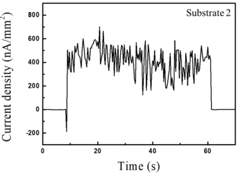
Fig. 3.3(d) shows the current measured through the copper wire placed on the substrate 2 during deposition. As shown in Fig. 3.3(d), an appreciable current was measured in the range of the deposition time from 10 to 60 sec, when the film was deposited, but the current was negligible when the film was not deposited, i.e. before 10 secs and after 60 secs. During the film deposition, the fluctuating current of several hundred nA was maintained with the current of up to ~700 nA/mm2being measured. It is assumed that the source of this current was positive charges carried by the secondary particles. Considering Fig. 3.3(a) and Fig. 3.3(d), it seems that positively charged secondary particles were the main flux of the dense film deposited on the substrate.
Fig. 3.4(a) shows a cross sectional TEM image of the Al2O3 film deposited on the substrate 2 when the bias of + 250 V was applied to one of the electrodes with the other grounded electrode during deposition. Even though the substrate 2 was placed in the same position as that of Fig. 3.3, the film deposited by the secondary particles in Fig. 3.4(a) was not dense but porous, with numerous voids indicated by the arrows. Besides, the identity of individual particles could be clearly distinguished in the TEM image in Fig.
47
3.4(a), whereas it was not distinguished in Fig. 3.3(a). Therefore, the crystallite size is much larger in Fig. 3.4(a) than in Fig. 3.3(a).
As expected in Fig. 3.2, the amount of the deposited flux in Fig. 3.4(a) was much smaller than that in Fig. 3.3(a), indicating that the majority of secondary particles were deflected by the electric field.
A single secondary particle is indicated in the white dashed circle in the bright-field TEM image of the film in Fig. 3.4(b). This particle seems to be very close to a single crystal considering the contrast difference. It is unclear whether all the individual particles were a single crystal, but it was confirmed that they maintained a certain degree of single crystallinity. For example, the SAED pattern of Fig.
3.4(c) also showed that the film had high single crystallinity.
Comparing Fig. 3.3(b) and Fig. 3.4(b), the grain size in Fig. 3.4(b) is much larger than that in Fig. 3.3(b). Considering that the secondary particles would have similar size between Fig. 3.3(a) and Fig. 3.4(a), the reduction of the crystallite size in Fig. 3.3(a) indicates that appreciable plastic deformation occurred, whereas it did not in Fig.
3.4(a). The absence of voids in Fig. 3.3(a) and their presence in Fig.
3.4(a) also indicate that appreciable plastic deformation occurred in Fig. 3.3(a) whereas it did not in Fig. 3.4(a).
The current measured during deposition through the copper wire on the substrate 2 is shown in Fig. 3.4(d). The measured current in
48
Fig. 3.4(d) was smaller than that in Fig. 3.3(d) by more than one order of magnitude. The current in Fig. 3.4(d) was close to zero in the scale of Fig. 3.3(d) and fluctuated occasionally, but did not exceed several tens of nA as shown in the inset with the magnified y axis.
Under the condition where the electric bias of +250 V was applied to one of the electrodes, the electric field is formed between the two electrodes. The electric field is roughly vertical to the trajectory of the secondary particles. Therefore, if secondary particles are charged, they would be deflected by the electric field. As a result, mainly neutral secondary particles would be deposited on the substrate 2.
The significantly reduced flux for deposition in Fig. 3.4(a) and the significantly reduced current in Fig. 3.4(d), together with Fig. 3.2(b) and (c), indicate that most of secondary particles were positively charged and deflected in the electric field. Therefore, it is thought that the secondary particles deposited on the substrate 2 under the condition of the electric bias would be mainly neutral. Fig 3.4(a) shows that distinguishable secondary particles, which were mainly neutral, were just accumulated on the substrate. On the other hand, Fig. 3.3(a) shows that the secondary particles, which were positively charged, underwent plastic deformation and fusion. These results
49
show that the presence of charge is responsible for the evolution of dense films in the AD process.
Then, why is the film in Fig. 3.4(a) not dense but porous? And why is the film in Fig. 3.3(a) dense when the electric bias is not applied?
These questions are important, because the answers might be related to the mechanism of the dense film evolution by AD. Considering Fig.
3.3(a) and Fig. 3.4(a), secondary particles, which were deflected by the electric field, appear to contribute to the evolution of dense films.
Secondary particles, which had not been deflected by the electric field and produced the film in Fig. 3.4(a), differ from those deflected by the electric field in that they are mainly neutral. In other words, the secondary particles deflected by the electric field have the characteristics of positive charge, which seems to be responsible for the evolution of dense films by AD. For the dense film to be evolved by the deposition of charged nanoparticles, some plastic deformation should occur.
50
Figure 3.2 TEM images of (a) an original Al2O3 particle with the inset indicating its SAED pattern, (b) secondary nanoparticles captured on the positive electrode, and (c) secondary nanoparticles captured on the grounded electrode
51
Figure 3.3 (a) Cross sectional TEM image of the Al2O3film deposited on the substrate 2 under the condition where the bias was not applied to the electrode, (b) high magnification bright field TEM image of the film in (a) with a dark single grain indicated in the dashed circle, (c) SAED pattern of the film, and (d) current measured at the substrate 2 during deposition
52
Figure 3.4 (a) Cross sectional TEM image of the Al2O3film deposited on the substrate 2 under the condition where the bias of + 250 V was applied to the electrode, (b) high magnification bright field TEM image of (a) with a dark single grain indicated in a dashed circle, (c) SAED pattern of the film, and (d) current measured at the substrate 2 during deposition
53
4. Conclusion
A dense Al2O3 film was deposited by secondary nanoparticles generated during AD. Secondary particles were mainly positively charged, and some were considered neutral. Neutral secondary particles did not form a dense film and seemed to maintain their shape and crystallinity after deposition. Considering the experimental and calculation results, it is thought that the positive charge, carried by the secondary nanoparticles and originated by the loss of electrons by fracto-emission during fracturing of aerosol Al2O3 particles, induces plastic deformation by decreasing the GSF energy and makes it possible for the dense film to be evolved during AD.
54
Chapter 4. Positive charge effect on plastic deformation of Al 2 O 3
(ab-initio calculation)
55
Chapter 4. Positive charge effect on plastic deformation of Al
2O
3(ab-initio calculation)
4.1 Introduction
Controlling the mechanical properties of ceramic materials is especially important for commercial applications due to their high brittleness and low fracture toughness.
Several studies on the effects of charging on material processing have been published [36, 44-46]. Using in-situ compression and tensile tests inside transmission electron microscopy, Zheng et al. reported that electron-beam irradiation could induce superplastic deformation of amorphous silica [47]. Using in-situ TEM observation during tensile tests, Zheng et al. also observed super-elongation of polycrystalline Li2O nanowires under electron beam irradiation compared to that without e-beam irradiation [48]. In the case of bulk ceramics, the elongation of the fine-grained Al2O3
and 3Y-TZP specimens increased under electrical field compared to without the electrical field [49].
Density functional theory (DFT) calculations by Shen et al. revealed that the mechanical properties of ionic semiconductor materials like ZnS, ZnTe, and CdTe are affected by charge carrier concentration [50]. Despite these studies, it is still unclear how charging affects the mechanical characteristics of oxide materials. To investigate the charging effects on oxides using DFT calculations, Al2O3was used as a model system because both experimental and theoretical methods have been extensively studied about a charge-neutral system[51-55]. The dislocations and twins in sapphire are formed by three critical slip systems: basal, pyramidal, and prismatic slips. By analyzing the generalized-stacking fault (GSF) energy calculation
56
for three slip systems, the charge-dependent mechanical properties of Al2O3 are examined. Electrons were removed from the periodic bulk Al2O3 lattice without vacuum space to simulate the mechanical properties of Al2O3upon charging.
4.2 Computational method
All calculations were performed using the spin-polarized density functional theory (DFT) implemented in the Vienna Ab-initio Simulation Package (VASP).[56, 57] To calculate the exchange- correlation interactions, the generalized gradient approximation (GGA) functional of Perdew–Burke–Ernzerhof (PBE)[58] was used combined with a projector-augmented wave (PAW) method.[59, 60]
To calculate the electronic wave functions, plane waves with an energy cutoff of 450 eV were used. In the surface Brillouin zone (SBZ) of the surface unit cell, the k-space integration was performed using a 3 × 3 uniform grid. The geometry was optimized until the remaining atomic forces became smaller than 0.01 eV/ Å . Theoretically optimized lattice constants of α-Al2O3 were obtained before the generalized stacking fault (GSF) energy calculations. The optimized lattice parameters were a = 4.80 Å, and c = 13.09 Å for the hexagonal close packed (HCP) unit cell in good agreement with the results of previous studies[61, 62].
57
Three crucial slip systems form the dislocations and twins in Al2O3: basal, pyramidal, and prismatic slips. In the previous study, the excess positive charging effects on the stacking fault energy of the basal slip system were studied by DFT calculation[63]. In this study, the excess positive charging effects on the stacking fault energies of three slip systems (basal, pyramidal and prismatic) were investigated. To calculate the GSF energy, we constructed a supercell with certain crystallographic directions, depending on the slip system to be studied, in which parts of atomic layers were rigidly translated by a displacement toward a specific direction on a particular lattice plane. Bulk systems that periodically repeated along the x, y, and z directions were used. To modify the sequential stacking fault energy change from the perfect crystal structure, we divided the unit cell into two blocks in each slip system, generating two energetically identical stacking faults. During the slip, one block was fixed in its equilibrium position, while the other was displaced from the perfect crystal to intrinsic stacking fault structure along the Burgers vector ⃗. From the perfect crystal to intrinsic stacking fault structure, we created six fault structures to calculate the energy barrier of stacking fault nucleation. For basal slip systems, the optimized atomic positions and total energies were calculated while four O and three Al layers were frozen in their equilibrium bulk
58
positions in each block and the other three Al layers near the stacking fault plane were relaxed in both sides[63]. For pyramidal slip systems, the optimized atomic positions and total energies were calculated while four O and two Al layers were frozen in their equilibrium bulk positions in each block and the other four Al layers near the stacking fault plane were relaxed in both sides. For prismatic slip systems, the optimized atomic positions and total energies were calculated while four O and one Al layers were frozen in their equilibrium bulk positions in each block and the other two Al layers near the stacking fault plane were relaxed in both sides. We removed one to three electrons from the supercell to simulate the change of the hole concentration.
59
4.3 Results and discussion
We examined the effect of positive charging on the GSF energy of an Al2O3 supercell along main slip paths in the HCP lattice: (1) (0001) [1120] of a basal slip, (2) (0112) [0111] of a pyramidal slip, (3) (1210) [0110] of an asymmetric prismatic slip while slicing the (1210) plane between the Al and O layers, and (4) (1210) [0110] of a symmetric prismatic slip while slicing the (1210) plane between two Al layers.
The Burgers vector of the perfect dislocation of the basal slip can be divided into the Burgers vectors of two energetically favorable partial dislocations as follows:
1
3[1120] →1
3[1010] +1
3[0110]
Since the GSF energies of the two partial slips are identical, only one of the partial dislocation displacements along the Burgers vector was considered to obtain the parameters of the basal slip. Fig. 4.1(a) shows the sequential changes in the structure during the slip along the basal plane.
The pyramidal slip is the only dislocation system that has the [0001]
component in its Burgers vector. There are several possible Burgers vectors in pyramidal dislocations, and the [0111] direction is most
60
beneficial energetically. Fig. 4.1(b) shows the sequential changes in the structure during the pyramidal slip along [0111].
The Burgers vector of the perfect dislocation of the prismatic slip can be divided into the Burgers vectors of three energetically favorable partial dislocations with sequential generation of stacking faults as follows:
[0110] →1
3[0110] +1
3[0110] +1
3[0110]
Two prismatic slips were considered according to the position of the slip plane. The first was the asymmetric prismatic slip in which the slip plane was located between the Al and O layers, as shown in Fig. 4.1(c). The second was the symmetric prismatic slip in which the slip plane was located between the two O layers, as shown in Fig.
4.1(d). Figs. 4.1(c) and (d) show the sequential changes in the structure during the prismatic slip.
To examine the positive charging effects, we extracted one to three electrons per 90 atoms from