Regular Paper 32 J. KIEEME
Vol. 24, No. 1, pp. 32-35, January 2011 DOI: 10.4313/JKEM.2011.24.1.32
상부 발광 유기 발광 소자에서 두께와 시야각에 따른 마이크로 캐비티 특성
이 원 재1,a
1 경원대학교 전자공학과
Thickness and Angle Dependent Microcavity Properties in Top-Emission Organic Light-Emitting Diodes
Won-Jae Lee1,a
1 Department of Electronic Engineering, Kyungwon University, Seongnam 461-701, Korea (Received November 8, 2010; Revised November 17, 2010; Accepted December 6, 2010)
Abstract: Top-emission device has a merit of high aperture ratio and narrow emission spectrum compared to that of bottom-emission one. Emission spectra of top-emission organic light-emitting diodes depending on a layer thickness and view angle were analyzed using a theory of microcavity. Device structure was manufactured to be Al (100 nm)/TPD/Alq3/LiF (0.5 nm)/Al (2 nm)/Ag (30 nm).
N,N'-diphenyl-N,N'- di (m-tolyl)-benzidine (TPD) and tris (8-hydroxyquinoline) aluminium (Alq3) were used as a hole-transport layer and emission layer, respectively. And a thickness of TPD and Alq3 layer was varied in a range of 40 nm~70 nm and 60 nm~110 nm, respectively. Angle-dependent emission spectrum out of the device was measured with a device fixed on a rotating plate. Since the top-emission device has a property of microcavity, it was observed that the emission spectrum shift to a longer wavelength region as the organic layer thickness increases, and to a shorter wavelength region as the view angle increases. Layer thickness and view-angle dependent emission spectra of the device were analyzed in terms of microcavity theory. A reflectivity of semitransparent cathode and optical path length were deduced.
Keywords: Microcavity, Top-emission, Spectrum, Angular
1. 서 론1)
현대 사회는 정보 통신 기술이 고도로 발달하고 정 보화 사회로의 움직임이 가속화되면서 기존의 디스플 레이 소자와는 다른 새로운 경쟁력을 가진 고성능, 저비용의 차세대 디스플레이 연구 개발이 중요시 되 고 있다. 차세대 디스플레이로서 주목받고 있는 유기 발광 소자는 자발광으로서, 타 디스플레이보다 두께
a. Corresponding Author; [email protected]
가 얇고, 밝기 변화에도 동일한 색상을 유지하는 면 발광 소자이다. 또한 응답 속도가 빠르며, 고효율과 고해상도로 자연색에 가장 가까운 화면 표시 소자 이다.
유기 발광 소자는 1963년 Helfrich 그룹에 의해 안트 라센 단결정에서 발광을 관찰되었다. 1987년 Tang과 VanSlyke는 적층 구조의 소자를 발표하였으며 [2], 그
이후 유기 발광 소자의 연구는 더욱 활발하게 되었다.
상부 발광 유기 발광 소자에서 발광 스펙트럼은 발 광층의 물질, 유기물층의 두께 및 소자 구조 등에 의
전기전자재료학회논문지, 제24권 제1호 pp. 32-35, 2011년 1월: 이원재 33
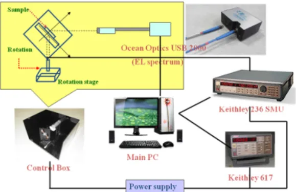
Fig. 1. Top-emitting device structure used in our study.
Fig. 2. Electrical and optical measurements.
Fig. 3. Device model for an understanding of theoretical cavity formula.
해서 결정된다 [3-5]. 또한 소자에 사용한 전극의 반 사도가 적절히 크면, 발광 스펙트럼의 변화가 일어난 다. 이러한 변화는 마이크로 캐비티 효과에 의하여 발생한다. 1994년에 Dodabalapur 그룹은 하나의 발광 층을 사용한 마이크로 캐비티 효과를 이용하여 다양 한 스펙트럼을 가지는 소자를 발표하였다 [6,7]. 마이 크로 캐비티 효과의 장점은 하나의 발광층으로 전극 의 반사도와 유기물층의 두께를 조절하여, 반폭치가 좁은 스펙트럼과 봉우리 파장의 변화를 가져올 수 있 다는 점이다. 또한 폭이 좁은 스펙트럼은 고해상도 디스플레이에 적합하다. 이후로 마이크로 캐비티 효 과의 연구는 계속 발전해 왔다 [8-10].
본 논문에서는 유기물층의 두께와 시야각 변화를 통하여 나타나는 상부 발광 유기 발광 소자의 광학적 특성을 마이크로 캐비티 이론으로 이해하고, 반투명 음전극의 반사도와 소자 내부에서 광학적 거리를 유 추하였다.
2. 실험 방법
소자 구조는 그림 1에서 보는 바와 같이 Al (100 nm)/TPD (x nm)/Alq3 (y nm)/LiF (0.5 nm)/Al (2 nm)/Ag (30 nm)로 하였다. 증착된 Al 100 nm 위에 정공 수송층인 N,N'-diphenyl-N,N'-di (m-tolyl )-benzidine (TPD) 를 40 nm~70 nm까지, 그리고 발 광층으로 사용한 tris (8-hydroxyquinoline) aluminium (Alq3)는 60 nm~110 nm까지 열증착하였다. 반투명 음전극은 LiF/Al/Ag를 사용하였다. 증착은 2 x 10⁻⁵ torr의 진공에서 하였고, 증착 속도는 유기물층은 0.
5~1.0 Å/s, 그리고 전극은 0.5~5 Å/s로 하였다. 소 자의 발광 면적은 3 x 5 mm2로 하였다.
제작된 소자를 측정하기 위해 그림 2와 같이 장치
를 구성하였다. 소자의 구동은 Keithley 236 (source- measure unit)과 617 (electrometer)을 사용하였다. 시 야각에 따른 발광 스펙트럼은 회전 기판 위에 소자를 고정시켜 놓고, 0˚~60˚까지 기판을 회전시키며 Ocean Optics USB 2000을 사용하여 측정하였다.
3. 결과 및 고찰
⊥⊤ ⊤⊥
⊤ ⊥
⊤
⊥ ⊥ ⊥
(1)
제작된 소자의 발광 스펙트럼은 시야각이 증가함에 따라 단파장으로, 유기물층의 두께가 증가함에 따라 장파장으로 이동되는 마이크로 캐비티의 특성을 보인 다. 다음은 캐비티 구조에서 스펙트럼 Iout (λ)를 나 타내는 이론적인 식이다.
여기서 T는 반투명 전극의 투과도, R은 반투명 전극
34 J. KIEEME, Vol. 24, No. 1, pp. 32-35, January 2011: W.-J. Lee
Fig. 4. Emission spectra depending on the thickness of top-emission organic light-emitting diodes in a direction normal to the surface.
Table 1. Values of each parameter used in microcavity formula.
Thickness
peak ⊥ ⊤ ⊥ ⊤
Spectrum
(519 nm) 1 0.85 55 100 2.1 0.35 1
Spectrum
(562 nm) 1 0.85 70 130 2.4 0.42 1
Spectrum
(613 nm) 1 0.85 85 150 2.65 0.43 1
Spectrum
(655 nm) 1 0.85 95 170 2.7 0.48 1
(a)
(b)
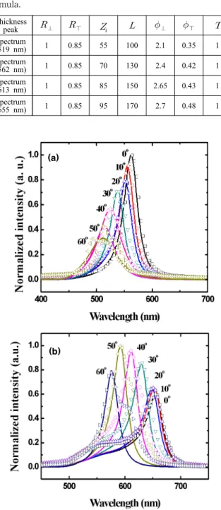
Fig. 5. Angle-dependent emission spectra of the top-emission organic light-emitting diodes for an organic layer thickness of (a) 130 nm and (b) 170 nm.
과 반사 전극의 반사도, zi 는 발광층의 실제 발광이 일어나는 지점에서 반사 전극까지의 거리, θi 는 내부 에서의 입사각, L 은 소자 내부에서 광학적 두께, 그 리고 Inc (λ)는 발광층 자체의 PL 스펙트럼이다. 식 (1)의 이해를 돕기 위해 소자 모형을 그림 3에 나타 내었다. 소자의 외부에서 시야각 θ 인 방향에서 스펙 트럼을 측정하였을 때, 내부에서의 입사각 θi 와는 스 넬의 법칙을 만족하게 된다. 즉,
(2)
이다.
그림 4는 상부 발광 소자의 두께에 따라 정면에서 얻은 (θ=0) 발광 스펙트럼이다. 유기물층의 전체 두 께를 100 nm에서 170 nm까지 증가시켰을 때, 봉우리 파장이 장파장으로 이동하는 모습을 보이고 있다. 점 선은 실험으로 얻은 파장에 따른 발광 스펙트럼이고, 실선은 식 (1)을 이용하여 광학적 거리를 100 nm에 서 190 nm으로 대입하고, 반사 전극의 반사도를 100%
로 하였으며, 반투명 전극의 반사도를 85%로 했을 때, 파장에 따라 나타나는 발광 스펙트럼이다. 식 (1) 을 사용하여 스펙트럼을 피팅할 때, 사용한 변수들의 값은 표 1과 같다. 점선과 실선이 일치하기 때문에, 반투명 전극의 반사도를 예상할 수 있었으며, 소자 내에서 빛의 흡수가 거의 일어나지 않았다면 투과도 또한 15%가 될 것으로 예상된다.
그림 5 (a)와 (b)는 유기물층의 전체 두께가 130 nm
와 170 nm일 때의 시야각에 따른 상부 발광 유기 발 광 소자의 발광 스펙트럼이다. 점선은 실험으로 얻은 발광 스펙트럼이며, 실선은 식 (1)을 통하여 이론적으 로 피팅하여 얻은 파장에 따른 발광 스펙트럼을 나타
전기전자재료학회논문지, 제24권 제1호 pp. 32-35, 2011년 1월: 이원재 35
내었다. 소자의 정면에서 60˚까지 시야각에 따른 스펙 트럼을 살펴보면, 봉우리 파장이 시야각에 따라 단파 장으로 이동하는 모습을 확인할 수 있다. 실험과 이론 적인 식을 통한 스펙트럼이 일치하는 반사도는 85%로 서, 정면에서 예상한 값과 일치하였고, 광학적 거리는 145 nm와 167 nm로 실험 결과와 거의 일치하였다.
4. 결 론
본 논문에서는 Al/TPD/Alq3/LiF/Al/Ag 구조의 상 부 발광 유기 발광 소자에서 생기는 마이크로 캐비티 효과를 연구하였다. 발광 스펙트럼의 봉우리 파장은 유기물층의 두께가 증가함에 따라 장파장으로 이동하 고, 시야각이 증가함에 따라 단파장으로 이동한다. 이 들 현상은 마이크로 캐비티 식으로 이해할 수 있었으 며, 이론적인 접근을 통해 반사도 R과 광학적 거리 L 을 유추해 볼 수 있었다. 또한 예상한 반사도와 광학적 거리는 실험 결과와 이론적인 유추와 잘 일치하였다.
감사의 글
이 연구는 2010 년도 경원대학교 지원에 의한 결과 이다.
REFERENCES
[1] W. Helfrich and W. G. Schneider, Phys. Rev. Lett.
14, 7 (1965).
[2] C. W. Tang and S. A. VanSlkye, Appl. Phys. Lett.
51, 913 (1987).
[3] L. S. Hung, C. W. Tang, and M. G. Mason, Appl.
Phys. Lett. 70, 152 (1997).
[4] L. S. Hung, C. W. Tang, M. G. Mason, P.
Raychaudhuri, and J. Madathil, Appl. Phys. Lett. 78, 544 (2001).
[5] H. Yokoyama, Science, 256, 66 (1992).
[6] A. Dodabalapur, L. J. Rothberg, and T. M. Miller:
Electron. Lett., 65, 1000 (1994).
[7] A. Dodabalapur, L. J. Rothberg, T. M. Miller, and E.
W. Kwock, Appl. Phys. Lett.. 64, 2486 (1994).
[8] Zhijun Wu, Hengqun Guo, Jiaxian Wang, and Shiyoung Liu, J. Phys. D: Appl. Phys, 39, 5160 (2006).
[9] Wenfa Xie, Shufen Chen, Letian Zhang, and Shiyoung Liu, J. Phys. D: Appl. Phys., 40, 5888 (2007).
[10] H. C. An, S. H. Na, H. W. Joo, and T. W. Kim, Trans. Electr. Electron. Mater., 10, 28 (2009).