저작자표시-비영리-변경금지 2.0 대한민국 이용자는 아래의 조건을 따르는 경우에 한하여 자유롭게 l 이 저작물을 복제, 배포, 전송, 전시, 공연 및 방송할 수 있습니다. 다음과 같은 조건을 따라야 합니다: l 귀하는, 이 저작물의 재이용이나 배포의 경우, 이 저작물에 적용된 이용허락조건 을 명확하게 나타내어야 합니다. l 저작권자로부터 별도의 허가를 받으면 이러한 조건들은 적용되지 않습니다. 저작권법에 따른 이용자의 권리는 위의 내용에 의하여 영향을 받지 않습니다. 이것은 이용허락규약(Legal Code)을 이해하기 쉽게 요약한 것입니다. Disclaimer 저작자표시. 귀하는 원저작자를 표시하여야 합니다. 비영리. 귀하는 이 저작물을 영리 목적으로 이용할 수 없습니다. 변경금지. 귀하는 이 저작물을 개작, 변형 또는 가공할 수 없습니다.
i
석 . 박사 학위논문 등표지
F a brica tio n a nd E mp lo y men t o f O rg a nic t hin f ilm s f o r O rg a nic Li g ht E mitt ing Dio de s • M a ria M us ta fa • 2 0 1 4ii
A THESIS
FOR THE DEGREE OF DOCTOR OF PHILOSOPHY
Fabrication and Employment of Organic thin films
for Organic Light Emitting Diodes
Maria Mustafa
Department of Mechatronics Engineering
GRADUATE SCHOOL
JEJU NATIONAL UNIVERSITY
2014. 02
iv
To
v
Acknowledgements
Start with the name of Almighty Allah, the most merciful, the most beneficent. First
of all I would present my humble gratitude in front of Allah Who enabled me to
accomplish the dignified cause of education and learning and I would pray to Him
that He would make me able to utilize my knowledge and edification for the
betterment of humanity and its development. Most of all, I would like to first express
my appreciation to my parents for their encouragement, and endless love. Whenever
I am in trouble, their love always guides me on the road of life. I also thank my elder
sister and brother for motivating me to continue my studies.
I also thank all my committee members, Prof. Ki Rin Kwon, Prof. Yang-Hoi, Dr.
Doh, Jeongdai Jo, and Prof. Hong Dong Peoh for their advice and participation in the
review and evaluation of this work.
I again acknowledge Prof. Kyung Hyun Choi for giving me a plenty of chances to
test organic electronic devices fabricated by his group, providing access to his
students and laboratory equipments. His guidance and expertise allowed me the
chance to work efficiently. I also thank Prof. Jeongdai Jo for his advice about my
research and attitude for science.
Within the three years of graduate student life in Jeju National University, Jeju, I
owe my gratitude to a long list of people. I want to thank all past and current group
members Dr. Khalid Rehman, Dr. Nauman Malik, Dr. Naeem Awais, Dr.
Naveneethan, Adnan Ali, Muhammad Zubair, Kamran Ali, Murtaza Mehdi, Junaid
Ali , Shahid Aziz, Ghayas Siddiqi, Dr. Zahid Manzoor, Hougun Lee, Hyo-Kyun
vi
Contents
List of Figures ... vii
List of Tables ... ix
Abstract ...x
1 Introduction ...1
1.1 Organic Light Emitting Device ...2
1.2 Promising Materials for Organic Light Emitting Devices ...6
1.3 Fabrication Processes ...11
1.4 Electrospray Fabrication Technique ...15
1.1 Research Motivation and Thesis Outline ...18
2 Fabrication of Organic Thin Films ...21
2.1 Poly [2-methoxy-5-(2'-ethylhexyloxy)-(p-phenylenevinylene)] Thin Film 21 2.1.1 MEH-PPV Polymeric Thin Film Deposition ...24
2.1.2 Thin Film Characterization ...28
2.1.3 Conclusions ...35
2.2 Poly[9,9-dioctylfluorenyl-2,7-diyl]-co-1,4-benzo-(2,1,3)-thiadiazoleThin Film 36 2.2.1 F8BT Polymeric Thin Film Deposition ...39
2.2.2 Thin Film Characterization ...43
2.2.3 Conclusions ...51
2.3 2,9-dimethyl-4,7-diphenyl-1,10-phenanthroline Organic Thin Film ...51
2.3.1 Small Molecule based BCP Organic Thin Film Deposition ...54
2.3.2 Thin Film Characterization ...59
2.3.3 Conclusions ...63
3 Organic Light Emitting Devices Fabrication and Performance Evaluation using electrospray deposited Functional thin films ...65
3.1 MEH-PPV Polymer based OLED ...65
3.1.1 OLED Device Fabrication ...65
3.1.2 OLED Device Performance ...66
3.2 F8BT Polymer thin film based OLED ...67
3.2.1 OLED Device Performance ...67
3.2.2 OLED Device Performance ...69
3.3 F8BT Polymer thin film based OLED with BCP as EIL ...70
3.3.1 OLED Device Preparation ...70
3.3.2 OLED Device Performance ...70
3.4 Conclusions ...74
4 Executive Summary ...75
5 Future Work ...79
vii
List of Figures
Figure 1-1: Cross section schematic of a typical organic light emitting device. ...3
Figure 1-2: Working principle of OLED Device. ...4
Figure 1-3 Schematic Energy Level Diagram of OLED device. ...4
Figure 1-4: Examples of commercial opportunities for organic electronics. ...5
Figure 1-5: Organic hole--(I--VI) and electron--conducting (VII-IX) materials employed for the fabrication of devices: (I) poly(phenylenevinylene) poly[2--methoxy--5--(3,7--dimethyloctyloxy)]-- 1,4--phenylenevinylene) (MDMO--PPV): R ’:-OMe; R: 3,7-dimethyloctyloxy); (II) polythiophene (poly(3-hexylthiophene) (P3HT): R: hexyl); (III) poly(fluorene-co- benzothiadiazone) (poly(9,9′- dioctylfluorene-co-benzothiadiazole) (F8BT) R: octyl); (IV-V) poly(triphenylamine) (triphenylamine moiety (IV) integrated in the polymer backbone and (V) as side chain); (VI) tetraphenylbenzylidendiamine (TPD); (VII) buckminsterfullerene C60; (VIII) 1--(3--methoxycarbonyl)
propyl--1--phenyl[6,6]C61 (PCBM),(IX) disubstituted perylene diimide derivative. ...10
Figure 1-6: Real-time photograph of the Spin coating deposition system and schematic illustration of deposition system. ...13
Figure 1-7: Real-time photograph of the Screen printing deposition system and schematic illustration of deposition system. ...14
Figure 1-8: Real-time photograph of the Langmuir-blodgett technique deposition system and schematic illustration of deposition system. ...14
Figure 1-9: Real-time photograph of the inkjet deposition system and schematic illustration of deposition system. ...15
Figure 1-10: Real-time photograph of the ESD deposition system and schematic illustration of deposition system. ...16
Figure 1-11: Mechanism of thin film fabrication process by electrospray. ...17
Figure 2-1: Mode of Electrostatic atomization of MEH-PPV ink; a) dripping, b) & c) micro dripping, d) pulsating unstable cone jet, e). stable cone jet , f) un-stable jet, g. ) multi-jet cone. ...28
Figure 2-2: Figure 3: Operating envelope of polymer ink. ...28
Figure 2-3: SEM images of the MEH-PPV thin films deposited at a standoff distance of 12, 15, 20 and 23 mm. ...30
Figure 2-4: AFM image of the MEH-PPV thin film deposited by electrospray...31
Figure 2-5: The XPS survey spectrum of MEH-PPV film deposited by ESD technique. ...32
Figure 2-6: Absorption spectra of annealed MEH-PPV onto ITO coated PET. ...33
Figure 2-7: (i) IV characteristics of MEH-PPV single layer deposited on glass substrate, (ii) IV characteristics of ITO/PEDOT:PSS/MEH-PPV organic diode in linear scale and (iii) IV characteristics of ITO/PEDOT:PSS/MEH-PPV organic diode in semilograthimic scale. ...34
Figure 2-8: Operating envelope of the F8BT polymer ink. ...43
Figure 2-9: E-spray Atomization modes; a. Dripping mode, b. Unstable Cone jet mode, c. Stable Cone Jet mode, d. Multi-Cone Jet mode. ...43 Figure 2-10: SEM image of F8BT film fabricated with the stand-off distance of: a. 19, b. 20 and c. 21 mm, and SEM image of F8BT film fabricated with; (d) single
viii
deposition pass, (e) two deposition pass, (f) three deposition pass; the inset shows the corresponding thickness of the film. ...45 Figure 2-11: Wide-scan XPS spectra of the e-sprayed deposited F8BT thin film; Inset shows the close up scan of the N 1s peak. ...47 Figure 2-12: Absorbance spectra of F8BT thin film for three different number of deposition passes...48 Figure 2-13: The pictorial picture of the ITO/PEDOT:PSS/F8BT/Al organic diode device. ...49 Figure 2-14: JV plot of the ITO/PEDOT:PSS/F8BT/Al organic diode having e-spray deposited F8BT thin film; a. in linear scale, b. in semilograthimic scale, c. in Log-Log scale. ...50 Figure 2-15: Operating envelope of the BCP organic ink. ...58 Figure 2-16: Functional spray modes; a. Dripping mode, b. Micro-dripping, c.
Unstable Cone jet mode, d. Highly Pulsating Cone jet mode, e. Stable Cone Jet mode, f. Multi-Cone Jet mode. ...58 Figure 2-17: SEM image of BCP film fabricated at the stand-off distance of 5 mm with the single-step deposition pass. ...60 Figure 2-18: Variation of the thin film of electrosprayed BCP with number of ESD deposition passes with moving substrate speed of 3mm/sec. ...60 Figure 2-19: Wide-scan XPS spectra of the e-sprayed deposited F8BT thin film; Inset shows the narrow- scan XPS spectra indicating N 1s peak. ...61 Figure 2-20: Absorbance spectrum of BCP thin film for four different number of
deposition passes; the insets shows theplotof(αhv)2 verses photon energy for BCP
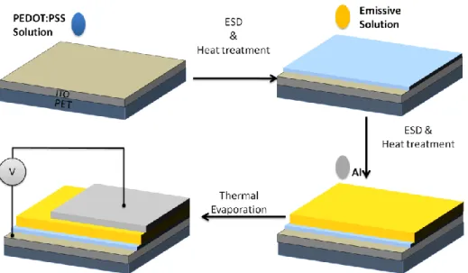
thin film of 75 nm thickness. ...63 Figure 3-1: Schematic diagram illustration of the fabrication process for
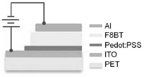
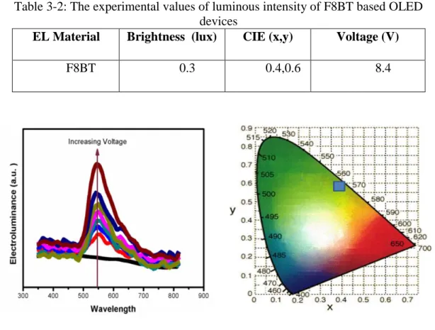
multi-layered MEH-PPV OLED device. ...66 Figure 3-2: Electroluminance of the OLED device at on state (left side) and CIE coordinates for OLED device having electrosprayed MEH-PPV as an active layer. .67 Figure 3-3: Optical Image of the orange light emission from the MEH-PPV based device. ...67 Figure 3-4: Schematic illustration of ITO/Pedot:PSS/F8BT/Al OLED device. ...68 Figure 3-5: Schematic diagram illustration of the fabrication process for
multi-layered F8BT OLED device. ...68 Figure 3-6: Electroluminance of the OLED device under forward bais (left side) and CIE coordinates for OLED device having electrosprayed F8BT as an active layer. ..70 Figure 3-7: Optical Image of the orange light emission from the F8BT based device. ...70 Figure 3-8: The pictorial view of the ITO/PEDOT:PSS/F8BT/BCP/Al organic diode device. ...71 Figure 3-9: Schematic diagram illustration of the fabrication process for
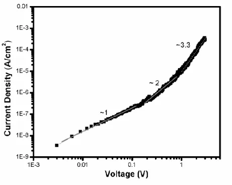
multi-layered F8BT OLED device having BCP as electron injection layer...72 Figure 3-10: J-V characteristics of the ITO/PEDOT:PSS/F8BT/BCP/Al organic diode having deposited BCP thin film in linear scale; the inset shows J-V plot of the fabricated organic diode in semilograthimic scale. ...72 Figure 3-11: Log-Log J-V plot of the ITO/PEDOT:PSS/F8BT/BCP/Al organic diode device. ...73
ix
List of Tables
Table 3-1: The experimental values of luminous intensity of MEH-PPV based OLED devices. ...66 Table 3-2: The experimental values of luminous intensity of F8BT based OLED devices ...69 Table 3-3: The experimental values of luminous intensity of F8BT based OLED devices with EIL ...73
x
Abstract
Organic light emitting diodes based lighting technology is focus of significant
academic research and industrial development interest, as they potentially offer
unique advantages over their inorganic counterparts in terms of cost reductions,
compatibility with low-temperature and printing-based manufacturing. Potential
applications of organic light emitting devices span a broad range of products
including displays, large area lighting, advertising, information, communication and
bio-sensing devices. Although a great progress has been made in this area so far, still
requires the search for alternative cost effective fabrication for the development of
these low cost organic electronics devices is vital in order meet the demand of
industrial large scale production. A wealth of solution processable materials has been
synthesized that hold key advantages such as reduced production cost, compatibility
with a vast range of substrates such as transparent glass and flexible polymeric
materials, and also open new doors to explore alternative low cost fabrication
methods.
In this thesis, fabrication methods of functional thin films of organic solution
processable materials have been reported and also their deployment for organic light
emitting diodes device fabrication from them. Thin films are deposited by
electrospray deposition technique in a vacuum-free environment using solution
processable materials’ inks as precursors. The effects of electrospray process parameters on film’s characteristics are described thoroughly. As a means of film
xi
analysis for organic light emitting diode device applications are reported. The results
obtained have showed that in terms of functionality, the thin films of solution
processing materials are suitable to replace their vacuum processed analogues as
building blocks in organic light emitting diodes devices. The work opens a
fabrication route for a next generation organic electronics device which could lead to
1
1 Introduction
Over the last 40 years, inorganic silicon and gallium arsenide semiconductors, silicon
dioxide insulators, and metals such as silver and copper have been the backbone of
the semiconductor industry. Silicon is the element central to the microelectronics
industry. However, although ideal for many integrated electronics applications,
single crystal silicon is not cheap, and the fundamental properties of silicon make it
unsuitable for the majority of optoelectronics applications. The use of lower quality
amorphous silicon avoids the costs associated with single crystal silicon, and is
suitable for cheap information-storing devices like smart cards and inventory control tags.Howeveramorphoussiliconrequiresaglasssubstrateto―grow‖on,whichis
not exactly ideal for a product to keep in your wallet, or for robust display screens of
laptop computers. Furthermore it is still incompatible with most optoelectronic
devices. That is why there is a growing scientific movement afoot to build circuits
made from entirely new materials – organic plastics. There has been a growing researcheffortin―organicelectronics‖ to improve the semiconducting, conducting,
and light emitting properties of organics (polymers, oligomers) and hybrids (organic–
inorganic composites) through novel synthesis and self-assembly techniques.
Performance improvements, coupled with the ability to process these ―active‖
materials at low temperatures over large areas on materials such as plastic or paper,
may provide unique technologies and generate new applications to address the
growing needs for pervasive computing and enhanced connectivity. Review on the
growth of the electronics industry clears that innovative organic materials have been
essential to the unparalleled performance increase in semiconductors, storage, and
2
materialsareeitherusedassacrificial stencils (photoresists) or passive insulators and
take no active role in the electronic functioning of a device. They do not conduct
current to act as switches or wires, and they do not emit light. Butinthelate1970’s
three scientists (Heeger, MacDiarmid, and Shirakawa) demonstrated that plastic can
be made to conduct electricity by manipulating its molecular structure, and shared
the 2000 Nobel Prize in Chemistry for their groundbreaking work. Building on their
findings, researchers continue to make advances at other institutions such as Lucent's
Bell Labs, Cambridge, IBM, Princeton, and Xerox PARC. The shift toward industrial
R&D is aided by the establishment of several government-sponsored research
initiatives, the founding of various organic electronics driven associations and
companies, and the development of IEEE standards for the testing of organic
electronics devices. The increased cooperative efforts between academia, industry,
and government are vital to the development of a strong materials and manufacturing
infrastructure.
1.1 Organic Light Emitting Device
Organic light-emitting device (OLED) based solid-state lighting technology
is one the most promising organic electronics based lighting technologies having
many superior advantages, such as lower power consumption, having very high in
color rendering index, transparent, dimmable, human-friendly, sustainable raw
materials, ultrathin, light weight, high contrast, fast response time and large view
angle. An OLED consists of very thin layers of organic films sandwiched by two
3
In OLED devices, organic electroluminescent materials, based on
π-conjugated molecules, are almost insulators, and light is produced by recombination
of holes and electrons which have to be injected at the electrodes. The anode is
transparent and is usually made of indium tin oxide (ITO), while the cathode is
reflective and is made of low work function metal. The general schematic working
principle and energy level diagram of OLEDs is presented in Fig. 1-2 and Fig. 1-3
respectively. When a voltage is applied between the electrodes, injection of holes
occurs from the anode and electrons from the cathode. Then, the charges move inside
the material, generally by hopping processes and then recombine to form excitons.
The location of the recombination zone in the diode is a function of the charge
mobility of the organic material as well as of the electric field distribution and is also
depend on the thickness of the electroluminescent materials layer (active layer).
After diffusion, the exciton recombines and photons are emitted of specific color
depending upon the difference between the highest occupied molecular orbital
(HOMO) and the lowest unoccupied molecular orbital (LUMO) levels of the
electroluminescent molecule. In order to obtain an efficient OLED comparable with
the inorganic LEDs, a multilayer stack of active materials is needed, having charge
injection, charge transporting and blocking properties.
4
Figure 1-2: Working principle of OLED Device.
Figure 1-3 Schematic Energy Level Diagram of OLED device.
Organic lighting diodes being emerging class of multidisciplinary research
field involves a series of conceptual, experimental and modeling challenging
regarding electronic devices incorporating carbon-based materials. The organic light
emitting devices are making their way onto market. This new field of electronics in
which the structures that are used are based on organic materials: dielectric,
conductive or semiconductor polymers or small organic molecules are deposited
5
Figure 1-4: Examples of commercial opportunities for organic electronics.
Organic materials can be made soluble and/or solution processable. This enables a
variety of deposition techniques that are not possible for conventional inorganic
semiconductor materials. Solution processability enables printing or printing like
processes. If one considers (conventional graphic) printing a manufacturing
processes, it is easy to realize that it must be one of the highest volume and lowest
cost manufacturing processes known. Printing presses commonly run at speeds of
hundreds of m/min. with webs several meters wide, and are used to deposit (and
cure) many different materials simultaneously. Printing produces large areas very
quickly and inexpensively. If one could use these processes (or ones like them) to
deposit functional materials, one could produce functional devices in high volume
very economically. Such is the appeal of organic electronics. Making this happen,
however, will require much effort and development, not only of new materials, but
also of thin film processes to be used for these materials. Like most other processes,
for optimal performance, the materials will need to be developed with the process
and conditions in mind.
Organic light emitting diodes with glass substrate are already used inside the
displays of smart-phones. But it is suitable for doing much more with plastic
6
roof lining, thus providing comfort and a feel-good atmosphere inside the vehicle.
OLEDs are suitable for various mobile devices displays such as blood glucose meters
or for patient monitoring. The latest applications for organic and printed OLEDs are
in e-book readers and touch screens with capacitive sensors. Few examples of
OLEDs towards devices applications are shown in Fig. 1-4.
1.2 Promising Materials for Organic Light Emitting Devices
Organic devices rely upon a wide variety of different types of electrically active
materials that has ability to process at low temperature sustained by plastic. Among
these materials, some of the most commonly used are conductors, semiconductors,
dielectrics, as well as various luminescent, electrochromic or electrophoretic
materials. Some type of supporting material is generally also used. Much other type
of materials can also be employed, such as surface active agents, encapsulation
materials, dopants, etc. Brief classification and description of these materials are
given below.
Conductors: Almost all printed devices require some type of electrode. The
electrodes may need to satisfy a number of requirements including low resistance,
smooth surface, chemical stability, and appropriate work function (the energy
required for an electron to escape a solid surface) for charge injection into the
semiconductor material. The materials used for conductors fall mainly into three
categories – those based on metals, organic compounds, and metal oxides. Metallic
features can be printed a number of different ways. The most common technique is to
use inks that contain metal particles. These particles may span a wide range of sizes
and morphologies. Nanoparticles can also be used, and subsequently sintered at plastic compatible temperatures (< 150˚C) to give electrically continuous features.
7
Metal precursors can also be used, sometimes in combination with other materials,
and similarly thermally cured. Another technique that has been used in the printing
of conductors is to print a seed layer, followed by plating another metal on top. In
this way, printing can be used to define the pattern, and the plating process can be
used to deposit a wide variety of metals, often much thicker than what could be
printed. The plating process can run at high volume. Even though certain polymers
can conduct electricity, they are still > 1000 times less conductive than metals. The
compounds that are most used for conductive polymers in printed are
hetero-aromatic polymers, based upon aniline, thiophene, and pyrole and their derivatives.
Of all of the conducting polymers, the one that has been used the most as a conductor
is probably PEDOT:PSS (which is commercially available. Dispersions of
PEDOT:PSS have good film forming properties, high conductivity (< 400 S/cm),
high visible light transmission, and excellent stability. Films of PEDOT:PSS can be heatedinairat>100˚Cfor>1000hourswithonlyminimalchangeinconductivity
Another class of conductive materials that is often used for electrodes are metal
oxides, particularly Indium Tin Oxide (ITO). These materials are used primarily
because of their transparency. They are used where transparent electrodes are needed, particularly for light emitting or optoelectronic devices. ―They are widely
used high- and low-tech applications such as antistatic coatings, touch display panels, solar cells, flat panel displays, heaters, defrosters, and optical coatings‖. Flexible
substrates (polyethylene terephthalate, PET) coated with ITO are commercially
available.
Semiconductors: Many organic electronic devices use semiconductors in one or
8
because it is where the mobile charge carrying species are formed and transported.
Semiconducting organic and carbon based materials are currently of broader interest
being potential low-cost materials for printable next generation organic electronic
applications. The studies of these materials are being carried out extensively in last
few years to build devices with a flexibility and softness. On one side materials of
polymers has been synthesized and developed day by day and on the other a large
focus has been devoted to the exploration of the enhanced properties of the hybrid
form of these polymers with inorganic materials. Carbon-based materials are
different that conventional in-organic materials like silicon or germanium in many
aspects. Usually they are categorized as small molecules and polymers, Polymer
semiconducting materials have the electronic properties of semiconductor and can be
fabricated with ease of processing in solution phase. The main advantage of the
utilization of polymers is their vast applications towards next generation flexible
electronic as the curing temperature of these materials are very low. Another
important motivation for interest in carbon based semiconducting materials is the
expected low cost of the end product of organic devices. Another important
motivation for interest in carbon based semiconducting materials is the expected low
cost of the end product of organic devices.
It is desirable to have electrical contacts between the semiconductor and the
electrodes that are ohmic and have a small contact resistance. Similarly, it is
desirable that the material be extremely pure, to eliminate inadvertent sources of
traps for the mobile charges. The charge transport in organic semiconductors is
highly dependent upon the deposition conditions, and can be influenced by many
9
temperature, surface treatment, surface roughness, etc. Environmental conditions can
also be a major factor, however, some organic semiconductors are air stable and don’trequireencapsulationoraninertenvironmentto maintain their performance.
For optimal charge transport, the molecular planes should be parallel to each
other and as close together as possible. In this situation, the charge will be
transported optimally in a single direction (the direction of the intermolecular
overlap). In order to make use in a practical device, the direction may also need to be
oriented with an appropriate direction in the device, for example, from the source to
the drain electrode in a transistor. So not only do the molecules need to be aligned
appropriately with each other, they also need to be aligned appropriately with respect
to the electrodes.
Many different families of organic semiconductors can be used, including
small molecules (pentacene and its derivatives), oligomers (primarily
oligothiophenes), and polymers (primarily polythiophenes). A large number of
luminescent organic semiconductors (both small molecule and polymer) have also
been developed for Organic Light Emitting Diode (OLED) applications. One of the
great advantages of organic semiconductors is that it is possible to chemically tailor
the structure of the molecule to achieve the desired properties. An important example
of this is the use of alkyl side chains to both improve the solubility, as well as to
induce molecular ordering, and thereby improve the molecular overlap and charge
mobility. In addition to organic semiconductors, nanoparticulate inorganic
semiconductors or hybrid organic-inorganic semiconductor materials have also been
used. These materials promise both the superior carrier mobility of inorganic
10
Figure 1-5: Organic hole--(I--VI) and electron--conducting (VII-IX) materials employed for the fabrication of devices: (I) poly(phenylenevinylene) poly[2--methoxy--5--(3,7--dimethyloctyloxy)]-- 1,4--phenylenevinylene) (MDMO--PPV): R’:--OMe; R: 3,7--dimethyloctyloxy); (II) polythiophene (poly(3--hexylthiophene)
(P3HT): R: hexyl); (III) poly(fluorene--co- benzothiadiazone)(poly(9,9′--dioctylfluorene--co--benzothiadiazole) (F8BT) R: octyl); (IV--V) poly(triphenylamine) (triphenylamine moiety (IV) integrated in the polymer backbone and (V) as side chain); (VI) tetraphenylbenzylidendiamine (TPD); (VII)
buckminsterfullerene C60; (VIII) 1--(3--methoxycarbonyl) propyl--1--phenyl[6,6]C61 (PCBM),(IX) disubstituted perylene diimide derivative.
Insulators or Dielectric: In general, a practical dielectric material should have a
high capacitance, high dielectric strength, high on/off ratio, high uniformity, high
dielectric breakdown, low hysteresis, and be defect free and easily processable. High
capacitance is important, because it allows a higher charge density to be induced at
lower voltages. This enables the reduction of the threshold and operating voltages,
while achieving this at a lower gate field. The capacitance can be increased by using
a thinner dielectric or by using a high permittivity insulator material. Unfortunately,
when the dielectric layer gets too small, breakdown and reliability issues (defects and
yield) can occur. Since the mobility of organic semiconductors is usually fairly low,
and the charge transport in organic semiconductors occurs within a few nanometers
11
dielectric, and particularly its surface, are critically important. A variety of materials
can be used as dielectrics. While much work has been done using inorganic (silica,
alumina, and high dielectric constant oxides) dielectrics, these are not generally
printable. A variety of organic polymers including polypropylene, polyvinyl alcohol,
polyvinyl phenol, poly methyl methacrylate, and polyethylene terephthalate can also
be used as dielectrics. Most of these are polymers that are widely used for non
electronic purposes and available in bulk quantities quite inexpensively.
1.3 Fabrication Processes
The outlook for low-cost production of light emitting diode based on organic
materials is a key driver for market opportunities in this area. To achieve these cost
targets, low-cost materials, cost-effective processes, and high-volume manufacturing
infrastructure are required. Organic light emitting diode has a high potential for
innovation with regard to the desired production process, printing technology. The
development of high-volume roll-to-roll manufacturing platforms for fabrication of
organiccircuitsoncontinuous,flexible,low-cost substrates, has been reported. Thin
organic films compatible to light emitting diode have many attractive features and
are being widely investigated for use in electronic devices. The production method is
simple, cost-effective and eco-friendly, thus allowing electronic components to be
produced in a way which is both ecologically and economically viable. When
components are printed using functional materials, an ink made from certain soluble
or dispersed functional material is used, which can then be processed in large
quantities using common printing processes such as screen printing or inkjet. The
12
printed on a large scale on a wide range of flexible substrates at relatively low
temperatures and then integrated into a wide range of products.
In OLEDs, there are three major types of considerations for determining the
printing process used. Techniques are chosen based upon their suitability for printing
the desired materials (viscoelastic properties), as well as by their capability to print
the desired feature sizes (lateral resolution, ink thickness, surface uniformity)
required by the device. Economic considerations such as process throughput are also
important. The printing processes with the highest resolution capability are also
generally those with the lowest throughput (and vice versa). The techniques having a
throughput > 1 m2/sec,areknownas―highvolume‖printingprocesses. These high
volume printing processes are highly desirable to enable the lowest cost production.
Solution processed deposition techniques used for thin film fabrication are highly
diverse in nature and include spin and spray techniques, Langmuir-blodgett, vacuum
filtration and inkjet printing. Different printing processes are discussed individually
as follows:
Spin coating: Spin coating is a technique, in which ink is applied to a rotating
substrate. The spread of the functional molecules occur due to the lack of centripetal
force inward centrifugal forces in the radial direction, thus leaving a fairly uniform
13
Figure 1-6: Real-time photograph of the Spin coating deposition system and schematic illustration of deposition system.
Screen Printing: Screen printing is a printing technique that uses a woven mesh to
support an ink-blocking stencil. The attached stencil forms open areas of mesh that
transfer ink or other printable materials which can be pressed through the mesh as a
sharp-edged image onto a substrate. A fill blade or squeegee is moved across the
screen stencil, forcing or pumping ink into the mesh openings for transfer by
capillary action during the squeegee stroke. Basically, it is the process of using a
14
Figure 1-7: Real-time photograph of the Screen printing deposition system and schematic illustration of deposition system.
Screen printing is more versatile than traditional printing techniques. The surface
does not have to be printed under pressure, unlike etching or lithography, and it does
not have to be planar. Different inks can be used to work with a variety of materials,
such as textiles, ceramics, wood, paper, glass, metal, and plastic. As a result, screen
printing is used in many different industries.
Langmuir-blodgett technique: With the Langmuir-blodgett technique, the substrate
is submerged into the liquid by hand and is pulled from the liquid to air to adsorb a
monolayer molecule of functional material, resulted in making the film of
micro-dimension on the substrate.
Figure 1-8: Real-time photograph of the Langmuir-blodgett technique deposition system and schematic illustration of deposition system.
Inkjet Printing :Most widely low cost techniques adopted for the fabrication of
these solution processed polymers are inkjet printing there by producing highly
efficient electronic devices. However in order to make uniform layer structure
devices with nanoscale dimensions, these technologies has their own inherent
difficulties and limitations with many pitfalls. For these reasons, the development of
15
the recent years. The most of the above criteria can be met in the method of electrospray
deposition.
Figure 1-9: Real-time photograph of the inkjet deposition system and schematic illustration of deposition system.
1.4 Electrospray Fabrication Technique
In an EHDA process, the ink containing the functional material is
continuously supplied to the metal capillary and is atomized into monodisperse
charged droplets of micron size under the influence of the electric field generated on
the droplet surface by the application of potential difference (voltage applied)
between the nozzle and grounded plate under stable cone jet mode. These droplets of
micron size are directed towards the substrate thus making a film of thin dimension
on the substrate. Recently, many researchers have applied the EHDA deposition
16
Figure 1-10: Real-time photograph of the ESD deposition system and schematic illustration of deposition system.
Comparing with other solution processed thin film fabrication techniques
like spin coating, air brush spray technique and vacuum filtration, EHDA technique
has potential to produce high quality nano-dimension thin film for large area
coverage thereby meeting the industrial scale up production and high throughput
demand using simple setup system. It has ability to produce nano-dimension
structures on several types of substrates without causing any type of damage to
substrates including flexible and also eliminates the problem of wastage of materials.
It provides opportunities for significant cost reduction in existing organic devices as
well.
Mechanism of ESD
The thin film fabrication by electrospray generally involved five processes shown in
Fig.1-11, which are
(1) Spray formation containing the fine droplets of the precursor liquid;
(2) Droplet transport from the nozzle to the substrate surface accompanied by
the evaporation of solvent and possible disruption of the droplets;
17
(4) The discharge of the impinged charged droplets, the spreading of droplet
solution on the surface, the penetration of the solution into the being- formed
layer, and a drying process; and
(5) the surface diffusion of solid particles, and physical interaction between
these particles [41].
Figure 1-11: Mechanism of thin film fabrication process by electrospray.
Factors affecting the growth, structure and film properties:
Various factors affect the growth, structure and properties of a deposited film. They are:
(i) nature of the substrate, (ii) substrate temperature, (iii) source temperature,
18
(iv) annealing,
(v) contamination by impurities and presence of defects on the substrate surface, and (vi) Presence of electrostatic charges etc.
The temperature of the substrate and thickness of the film are two very important parameters affecting its properties. The mobility of the just deposited material on the substrate surface can be enhanced by increasing the temperature of the substrates during the deposition process. Low mobility on the other hand leads to the formation of a film of amorphous nature. If the substrate is the face of a single crystal, periodic forces of cohesion induce an oriented growth called the epitaxial growth. Thus a thin film can be deposited in crystalline, polycrystalline and amorphous form.
1.1 Research Motivation and Thesis Outline
Conventional device fabrication is rather carried out using thin-film materials, which
can be integrated and patterned at the nanoscale with relative ease, and whose
preparation is cost-effective. The challenge that arises with the use of thin films for
nanoscale research and device applications lies, in general, with the greater
complexity of the thin-film surfaces relative to bulk materials. Typical thin-film
deposition procedures produce thin film surfaces, which normally demonstrate
significant topographic roughness on the nanoscale and highly variable atomic-scale
texture. For devices where the relevant interactions occur at the atomic and
molecular scale, the non-uniform surface structure of conventional thin-film material
surfaces can create significant issues for both understanding device behavior and
establishing device reproducibility.
To fully realize the potential of nanoscience research to generate device applications — and thus enable the commercial potential of nanotechnology — simple and
well-19
characterized thin-film material surfaces. The research presented in this thesis
therefore centers around the fabrication and detailed characterization of organic
thin-film material surfaces. The main objectives for the research herein were defined as
follows:
1. To develop techniques for fabricating thin-film organic material surfaces of
promise for nanoscale research and device applications.
2. To characterize the nanoscale physical and chemical properties of specifically
selected thin-film surfaces, chosen because of both their potential utility and the lack
of previous detailed examination.
3. To consider future applications in which the determined nanoscale properties of
the studied thin-film surfaces could be advantageously employed.
For device applications where organic thin-film material surfaces could be
most valuable — specifically, optoelectronics, memories, sensors and nanoscale
electronics — the ability to integrate the thin-film surfaces with conventional silicon electronicsdramaticallyenhancesthesurfaces’potentialutility.Basedontheabove
objectives and this criterion, this thesis presents the fabrication and characterization
of organic semiconducting materials surfaces that are ultra-thin on the nanoscale. As
discussed throughout the thesis, each of these thin-film surfaces fabricated and
studied present distinct nanoscale physical and chemical surface properties that are
desirable for a variety of nanoscience research and device applications. Furthermore,
this selection incorporates representative thin-film having application towards
several organic electronic devices — including organic light emitting diode —
20
This thesis is structured into two experimental chapters (Chapters 2 and 3).
Each chapter examines a specific process for fabricating ultra-flat thin-film, and
includes the detailed characterization of at least one material of particular interest.
The layout of each chapter generally follows the sequence of the objectives listed in
the previous section. The start of every chapter provides general background on the
ultra-flat thin-film surface fabrication technique and particular surfaces explored
therein, along with the impetus underlying the selection of both for study. The film
formation processes are then presented, in conjunction with any experimental data
relating to process development. The experimental characterization of the select
thin-film surfaces follows next, along with the experimental characterization of other
21
2 Fabrication of Organic Thin Films
2.1 Poly [2-methoxy-5-(2'-ethylhexyloxy)-(p-phenylenevinylene)] Thin FilmConjugated polymer materials have been getting enormous attraction in polymer
based organic optoelectronic devices due to their efficient optoelectronic properties
as well as the ease of processing in solution phase [M. Kertesz et. al; 2005, C. Zhong
et. al; 2011, H. Spanggaard et. al; 2004]. On one side materials of polymers has been
synthesized and developed day by day [L. Zhao et.al.; 2011, T.W. Yoo et. al.; 2011,
A. Swinarew et.al.; 2011, O. Lavastre et. al.; 2004, P.R. Andres et.al.; 2004] and on
the other a large focus has been devoted to the exploration of the enhanced properties
of the hybrid form of these polymers with inorganic materials [J.A. Ayllon et.al.;
2009, S. Kumar et.al.; 2004, A. Petrella et. al.; 2005, R. Taylor et. al.; 2007, C.
Ton-That et. al.; 2008]. The main advantage of the utilization of polymers is their vast
applications towards next generation flexible electronic as the curing temperature of
these materials are very low.
MEH-PPV polymer has been intensively studied because of its broad
applications in organic devices. MEH-PPV is characterized by a pi-conjugated
backbone in which the pi-electrons are delocalized over several monomer units along
the carbon chains, forming pi-bands. Because the delocalized orbital are half filled,
the energy gap between the filled and empty bands results in semiconducting
properties. The extent of delocalization of the pi-electrons, the so called conjugation
length, determines the energy gap, which plays a major role in the optical and
electrical properties of the materials and the performance of the organic devices they
22
Most widely low cost techniques adopted for the fabrication of these solution
processed polymers are inkjet printing [J. Bharathan et. al.; 1998, S.C. Chang et. al.;
1998, S. C. Chang et. al.; 1999, B.C. Krummacher et. al.; 2006, Y. Liu et. al.; 2003,
K.E. Paul et. al.; 2003], spin coating [T.S. Kang et. al.; 2003; N. Rehmann et. al.;
2007, S.A. Arnautov et. al.; 2004, W. Lee et. al.; 2008], there by producing highly
efficient electronic devices. However in order to make uniform layer structure
devices with nanoscale dimensions, these technologies has their own inherent
difficulties and limitations with many pitfalls [J. Sidén et. al.; 2007, S. Di Risio et.
al.; 2007, S.A. Jenekhe et. al.; 1984, W.W. Flack et. al.; 1984, K. Jong Lee et. al.;
2006, S. Ilkhanizadeh et. al.; 2007]. For these reasons, the development of
convenient low cost solution processing techniques has attracted more attention in
the recent years.
Electrospray deposition (ESD) has been extensively studied and investigated
as an alternative method for achieving the fabrication of thin films of valuable
materials [ S. Jayasinghe et. al.; 2004, A. Van Zomeren et. al.; 1994, P. Miao et. al.;
2001, D.H. Youn et. al.; 2009, A. Khan et. al.; 2011, A. Gupta et. al.; 2007, R.
Bakhshi et. al.; 2009, A. Khan et. al.; 2011, N.M. Muhammad et. al.; 2011, J. Ju et.
al.; 2009]. In the electrospray deposition process, an electric field is applied to a
pendant droplet of the precursor containing liquid solution generated at the tip of the
metallic nozzle by applying the potential difference of the order of kilovolts between
the metallic nozzle and the grounded electrode. The droplet thus deforms into a
conical shape, with a filament emanating from apex, known as cone-jet transition and
then at particular distances below the nozzle, this filament fans out in the form of the
23
that is being connected to the grounded electrode there by forming a thin film [H.F.
Poon et. al.; 2008, R. Hartman et. al.; 2006, K. Rahman et. al.; 2010, K.H. Choi et.
al.; 2010, O.V. Kim et. al; 2010, I. Hayati et. al.; 1986, T. Nguyen et. al.; 2001]. The
thin film fabrication by electrospray deposition technique generally involves five
processes which are (i) spray formation containing the fine droplets of the precursor
liquid; (ii) droplet transport from the nozzle to the substrate surface accompanied by
the evaporation of solvent and possible disruption of the droplets; (iii) the
impingement of the droplets on the substrate surface; (iv) the discharge of the
impinged charged droplets, the spreading of droplet solution on the surface, the
penetration of the solution into the being- formed layer, and a drying process; and (v)
the surface diffusion of solid particles, and physical interaction between these
particles [H.F. Poon et. al.; 2008]. The main advantages of ESD technology for the
fabrication of thin film include the possible tailoring of the morphology of the
deposited film [S. Gil Kim et. al.; 2000, N.M. Muhammad et.al.; 2011] and high
deposition efficiency since the electric field direct the charged droplets to the
substrate with a very simple setup architecture[N.M. Muhammad et. al.; 2011, T.
Nguyen et. al.; 2001, S. Gil Kim et. al.; 2000, N.M. Muhammad et.al.; 2011, K.H.
Choi et. al.; 2011]. Prior to ESD, the basic understanding of electrostatic spray of
liquid solution need to be investigated in order to fabricate the high quality thin film.
In this study, the understanding of electrostatic atomization of the in-house
developed ink was made by using ESD technology, followed by fabrication of the
thin polymer films. Polymer investigated for electrostatic atomization was
poly[2-methoxy-5-(2’-ethyl-hexyloxy)-1,4-phenylenevinylene] (MEH-PPV) and was
24
utilized extensively in many electronic devices [M. S. P. Sarah et. al.; 2010, N.
Kamarulzaman et. al.; 2011]. The operating envelope of ink was explored. Then the
thin film of polymer was prepared and was thoroughly characterized using different
thin film characterization tools. The surface morphology inspection was performed
by using JEOL JSM-7600F Field Emission Scanning Electron Microscope (FESEM)
machine operated at the accelerating voltage of 5 kV. For film thickness
measurement, thin film thickness machine K-MAC ST4000-DLX was used. The
surface roughness analysis was done by using PAFM S100 Atomic Force
Microscope (AFM). To look into elemental composition of the film, X-ray
Photoelectron spectroscopy (XPS) of the film was conducted using VG Microtech
XPS analysis equipment equipped with a monochromated X-ray source. Base
pressure during analysis was 1 × 10⁻⁷ Pa. For electrical characterization, the Agilent
B1500A Semiconductor Device Analyzer coupled with MST8000C Probe Station
having a current resolution of 1fA was used. Prototype organic diode devices with
structure of Indium Tin Oxide (ITO)/
Poly(3,4-ethylenedioxy-thiophene):poly(styrenesulphonate) (PEDOT:PSS)/ MEH-PPV were fabricated with
electrosprayed and spin coated MEH-PPV layers on Polyethylene terephthalate
(PET) separately. Then electrical characterization of diode devices was performed by
current voltage measurement and was compared.
2.1.1 MEH-PPV Polymeric Thin Film Deposition
MEH-PPV (Avg. Mol wt: 51000) powder and ITO coated PET substrate was
purchased from Sigma Aldrich company. The PEDOT:PSS (2.8% wt) (Orgacon) was
25
(DMF), Di-cholorobenzene (DCB), acetone and ethanol was purchased from Daejon
Chemical and Metal Co. Ltd., South Korea.
The solution having 0.4% of MEH-PPV concentration was prepared by dissolving
appropriate amount of MEH-PPV powder into the DCB solvent. Then the solution was subjected to stirring for 24 hours at the temperature of 80 ˚C. In order to get
powder completely dissolved, the solution was given the bath-sonication treatment for200minutesmaintainingthetemperatureof60˚C.Thepolymersolutionwasthen
allowed to cool to room temperature and was filtered using 0.2 µm syringe filters. At
the end, DMF solvent was added into the ink with the composition ratio of 1:3 of that
of polymer solution. The resultant ink was then used for ESD process. The viscosity
value of the ink was measured by Viscomate VM-10A and it was recorded to be 2.5
mPa. The surface tension measured from SEO’s contact angle analyzer was 27
mN/m. The dielectric value measured from BI-870 Dielectric Constant meter was
19.2. The electrical conductivity of the ink was measured by Conductivity meter
(Cond6+ meter) and its value was 2.5 µS/cm. The viscosity of the ink was kept low
in order to avoid electro-spinning phenomena induction [I.B. Rietveld et. al.; 2006,
C.H. Park et. al.; 2009].
The electrostatic atomization of MEH PPV ink was attempted using ESD system
[N.M. Muhammad et. al.; 2011]. The brief description of the system was as follows:
the ink solution was placed in the chamber (Nano NC Nozzle adapter) through
syringe pump (Hamilton, Model 1001 GASTIGHT syringe) and was provided at
constant rate to the nozzle through the syringe pump. The metal nozzle of 210 µm
internal diameter [Havard 33G] was used as anode and was connected to a Trek
26
was provided by connecting the ground terminal of the power source to the moving
stage and the substrate was placed on this moving stage. The speed of moving stage
was kept at 3 mm/sec. A high speed camera along with a light source was used in
conjunction with a portable computer to capture images of the electrostatic
atomization events. The flow rate with combination of voltage was used in order to
observe different modes of electrostatic atomization. The ink was subjected to
electrostatic atomization at 5 kV and 450 µl/hr under the stable cone jet mode. After
that, the distance between the capillary and the substrate was varied between 12 mm
to 23 mm in order to find the optimized distance followed by fabricating the film
keeping all other parameters of ESD constant. An ITO coated PET was used as
substrate and was cleaned with ethanol, acetone and deionized water respectively for
15 min each, dried and was subjected to spray. The resultant sample thus prepared
was thermally cured at 100 ˚C for 5 hours and was further used for surface
morphology analysis in order to investigate the quality of the film at each standoff
distance there by evaluating the optimized ESD parameters. By using optimized
parameters, the MEH-PPV thin films are prepared to observe the surface roughness
and thickness of the films. The samples on bare glass with slight different parameters
were also prepared and were used for single film XPS analysis, and electrical
measurement.
2.1.1.1 Ink Characterization and Spray Formation
The electrostatic atomization of the ink was investigated for the identification of an
operating envelope that can adopted while fabricating the thin film for the particular
electronic device applications. The electrostatic spray was first performed with
varying flow rate from 50 µl/hr to 450 µl/hr in order to determine optimum the
27
gradually increasing the potential difference between the anode nozzle and the
grounded stage [K. Rahman et. al.; 2010, K.H. Choi et. al.; 2010]. By varying the
potential difference, various modes of electrohydrodynamic phenomenon were
observed from dripping to multi-jet mode. Figure 2-1 shows the high resolution and
high speed images of different spray modes as achieved at different value of potential
differences keeping flow rate constant at 150 µl/hr. At zero potential difference,
dripping mode was only observed. Then the potential difference was gradually
changed from zero to 3.1 kV, only micro-dripping was observed. As the potential
difference was further increased, a pulsating cone jet was observed at 4.1 kV. Then at
potential difference value of 4.6 kV, a stable cone jet was witnessed which remained
until around 5.9 kV after that the multi-jetting was started. If the applied potential
difference was further increased, the jet discharged. A flow rate of 450 µl/hr has been
selected for the film fabrication. This value is selected as the droplet has directly
dependence on flow rate. However if the flow rate is too low, the stable cone jet
formation is going to be unstable after sufficient time span [N.M. Muhammad et. al.;
2011]. Figure 2-2 provides the observed optimum operating envelope of the
developed ink representing various atomization zones with varying flow rate and
28
Figure 2-1: Mode of Electrostatic atomization of MEH-PPV ink; a) dripping, b) & c) micro dripping, d) pulsating unstable cone jet, e). stable cone jet , f) un-stable jet, g. )
multi-jet cone.
Figure 2-2: Figure 3: Operating envelope of polymer ink.
The inequalities between electrical relaxation time (Tq) and hydrodynamic time (Th)
are a perquisite for the well established atomization phenomenon. The value of
electrical relaxation time must be much smaller than that of the hydrodynamic time.
Both Tq and Th depends on the ink properties as well as the on the ink jetting
behavior. At the flow rate of 150 µl/hr, the diameter of jet was 10µm and length of
jet was 600µm. With these values and the ink parameters, the value of Tq and Th
came out to be 7.977×10⁻⁶ and 1.4×10⁻⁴ respectively using the empirical relations
[N.M. Muhammad et. al.; 2011], which showed that the ink was satisfactory
fulfilling the criteria of electrical atomization.
2.1.2 Thin Film Characterization
29
The standoff distance is one of the important parameters of ESD technology and has
direct effect on the quality of the thin film. It determines the time of solvent
evaporation when droplet travel towards substrate. To see the effect of the stand-off
distance on the film quality, the electrostatic spray process was carried at four
different standoff distances of 12 mm, 15 mm, 20 mm, and 23 mm. The samples thus
prepared were subjected to SEM analysis. Figure 2-3 shows the effect of standoff
distances on the film morphology. At a standoff distance of 12 mm, the film was
highly porous and could be resulted due to the fact that the high amount of solvent
travelled down to the substrate and after drying left behind a large amount of empty
spaces on film. At the standoff distance to 15 mm, the quality of the film got
improved. The film was in the form of semi-liquid, and was not showing any wetting
problems, the solution flow or the rough grainy formations problem. It could be
easily seen at distance 15 mm that the quality of the polymer film was satisfactory
and free of pores. As the standoff distance was further increased, the pores started
appearing again and the quality of film become unsatisfactory. At this distance, the
film was formatted as a result of the evaporation of the most of the solvent during the
droplet flight causing to disturb the optimum ratio of polymer and solvent necessary
to form smooth film as well as restricting their spreading. The quality of film went
worse as the distance reached at 23 mm. An optimum distance from nozzle to
substrate was determined to be 15 mm at which the resulting film quality was
30
Figure 2-3: SEM images of the MEH-PPV thin films deposited at a standoff distance of 12, 15, 20 and 23 mm.
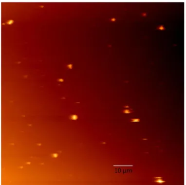
The surface roughness of the film was investigated by atomic force microscopy. The
AFM image over 100 µm x100 µm scan area was shown in Fig. 2-4. The AFM
image shows a smooth surface with the RMS value of 11.5 nm hence can be utilized
31
Figure 2-4: AFM image of the MEH-PPV thin film deposited by electrospray.
The average thickness of the MEH-PPV film measured by film thickness machine
was 168 nm ± 20 nm which is acceptable for the nanoscale electronic devices.
2.1.2.2 X-ray Photoelectron Spectroscopic Analysis
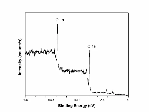
One of the issues related to electronic failures is the presences of solvent that remain
within the layers of electronic device during fabrication [S. Li et. al.; 2000]. In order
to confirm the complete removal of the solvent, the XPS survey spectrum analysis of
the electrospray deposited MEH-PPV film on glass was carried out and was shown in
Fig. 2-5. The figure indicates two prominent peaks which are ascribed to C and O
32
Figure 2-5: The XPS survey spectrum of MEH-PPV film deposited by ESD technique.
2.1.2.3 Optical Analysis
Figure 2-6 shows the absorption spectra of electro sprayed MEH-PPV thin
films within UV-visible range. MEH-PPV thin film gave broad peak above 350nm
centered at 495 nm wavelength which is associated to non-localized states (
HOMO-LUMO transition) [A. Marletta et.al; (2004)]. Overall the result suggests that the
33
Figure 2-6: Absorption spectra of annealed MEH-PPV onto ITO coated PET.
2.1.2.4 IV Analysis
In order to measure the conductivity of the polymer thin film, IV
characteristic curve for the single layer of electrosprayed MEH-PPV was recorded as
shown in Fig. 2-6(i). From the IV curve, the conductance of the film was evaluated.
Here the IV curve was presenting the semiconductor like behavior of MEH PPV
deposited film and the conductance of the film is calculated to be 7.14×10⁻⁵ Ω-1
which accords with that found in literature [ M. S. P. Sarah et. al.; 2010, N.
Kamarulzaman et. al.; 2011]
After the electrospray process was optimized, an ITO/PEDOT:PSS/MEH-PPV
organic diode was fabricated. The feasibility of electropsray for the multi-layered
structured diode was analyzed through its electrical characterization using
34
diode of same electronic structure was developed with spin coated MEH-PPV film
having comparative thickness to that of electrosprayed polymer layer and its
electrical performance was analyzed and compared.
Figure 2-7: (i) IV characteristics of MEH-PPV single layer deposited on glass substrate, (ii) IV characteristics of ITO/PEDOT:PSS/MEH-PPV organic diode in linear scale and (iii) IV characteristics of ITO/PEDOT:PSS/MEH-PPV organic diode
in semilograthimic scale.
Electrical behavior of the multi-layer film is very much dependent on the contact of
the two adjacent films and plays an important role in the performance of the
electronic device. The IV curve of the organic diode structures in linear scale,
recorded by semiconductor analyzer was shown in figure 2-7(ii) with electrosprayed
35
diode structure with sprayed MEH-PPV polymer film shows better performance. For
voltage 5 V, the current in organic structure with spin-coated polymer film is 7×10⁻³
A versus current in sprayed one, reaching about 1.6×10⁻² A there by indicating the
proper contact area of the uniformed electrosprayed layer with adjacent film in the
diode structure and resulting in increase charge carrier injection efficiency. The
organic diode having electrosprayed MEH-PPV film, showed typical Schottky diode
like behavior having a barrier height of 0.68 eV and ideality factor of 1.57 as
evaluated from the semilogarithmic plot of IV curve of the organic diode shown in
Fig. 2-7(iii). The experiment with electrospray deposition technology was repeated in
order to check the reproducibility of the process as shown in Fig. 2-7(ii). A relatively
small deviation (average 0.23 mA) was observed. The reason behind this deviation is
as the encapsulation of the structure was not performed, so there is possibility of the
impact of contamination from the environment on the electronic structure
performance which will be well thought-out as a part of future work.
2.1.3 Conclusions
In conclusion, the electrospray atomization of polymer ink has been achieved there
by fabricating defect free MEH-PPV nano scale thin layer. The effect of standoff
distance on the film morphology was investigated and optimized to the value of 15
mm. The film of polymer fabricated by optimized ESD parameters was thoroughly
examined. The e-spray deposited MEH-PPV film showed the absorption edge at
wavelength of 495 nm. The electrical behavior of the thin polymer was that of
semiconductor nature showing a conductance of 7.14×10⁻⁵ Ω-1. Contact between the
two adjacent polymers layers in organic diode structure with electrosprayed
36
coated MEH-PPV layer as evident from the IV characteristic curve of organic diodes.
The reproducibly of the electrospray process towards organic diode fabrication was
evaluated and was found satisfactory. OLED device with thin electrosprayed
MEH-PPV emissive layer show good current transporting anad electroluminance properties
because of proper contact between the adjacent layers in OLED structure. Overall the
results achieved highlights electrospray deposition as a key and promising
technology in the production of polymer nano thin films for organic diode structures
in environmental friendly manner.
2.2 Poly[9,9-dioctylfluorenyl-2,7-diyl]-co-1,4-benzo-(2,1,3)-thiadiazoleThin Film
The development and commercialization of polymer semiconductors have made
revolutionary progress due to the rapidly growing demand for printed electronic
applications [J. M. Shaw et.al; 2001]. Being low temperature and solution
processable, polymer materials have been gaining considerable interests to develop
organic electronic devices for future printable electronics [P. Leclere et. al; 2006, M.
Friedman et. al.; 2002]. Among them, the conjugated polymer
poly[9,9-dioctylfluorenyl-2,7-diyl]-co-1,4-benzo-(2,1,3)-thiadiazole (F8BT) has attracted
much attention because of its high long alkyl side chains that are introduced to
increase solubility and its wide band gap [ L. L. G. Justino et. al.; 2009]. Furthermore
it is relatively stable in air and its physical properties have been extensively studied
[M. Campoy-Quiles et. al.; 2005, S. Cook; 2003, J. K. Grey et. al.; 2006, C. R.
McNeill et. al.; 2006]. F8BT based devices has found their applications in the field of
organic light emitting diode lighting and display electronics [D. Kabra et. al.; 2010],