반도체디스플레이기술학회지 제19권 제1호(2020년 3월) Journal of the Semiconductor & Display Technology, Vol. 19, No. 1. March 2020.
Recent Progress on Voltage Drop Compensation in Top Emission Organic Light Emitting Diodes (OLED)
Byoung-Seong Jeong
*†*†
Department of Hydrogen and Renewable Energy, Kyungpook National University
ABSTRACT
The voltage drop due to the thin cathode film at the large size top emission OLED panel was successfully compensated with making electrical contact between thin cathode and anode auxiliary electrode by 355nm wavelength of laser. It was found that the luminance uniformity dramatically increased from around 15% to more than 80% through this electrical compensation between thin cathode and anode auxiliary electrode. Moreover, the removing process for EL materials on the anode auxiliary electrode process by laser was very reliable and stable.
Therefore, it is thought that the EL removal method using laser to make electrical contacts is very appropriate to mass production for such a large size top emission OLEDs to obtain high uniformity of luminance.
Key Words : OLED, Voltage Drop, Top Emission, Electrical Compensation, Laser
1. Introduction
1Unlike LCD, OLED displays can realize true deep black and have a lot of excellent properties as a key information communication tool in the 4th Industrial revolution with fast response speed, high contrast ratio, excellent wide-angle dependency, wide color gamut [1-3]. It is also the only display that can realize form factor free among mass- produced displays [4,5]. Due to these various advantages, there is a great demand for OLED displays of small to medium size as well as large size.
Currently, the bottom emission method is mainly used for the commercialized large OLED TV [6].
However, as the resolution goes up, this bottom emission method may have a limitation in improving the lifetime of self-luminescent OLED because it is difficult to increase the aperture ratio due to the interference of the metal lines in TFT backplane [7]. One alternative to improve this constraint is the top emission method. That is, when the top emission is applied, the aperture ratio can be maximized without interfering with the lower metal lines, thereby
†
E-mail: [email protected]
reducing the current density applied to the pixel. However, the top emission method that can maximize aperture ratio causes luminance uniformity issues due to Voltage Drop by thin cathode [8,9].
Therefore, in this study, the Voltage Drop compensation method that can improve the luminance un-uniformity by thin cathode throughout the panel, which is one of the key issues in large size top-emitting OLED display, were analyzed and a better method among them was proposed.
2. Experiments
2.1 Voltage Drop Compensation Analysis There are several ways listed in Table 1 to compensate the Voltage(IR) Drop, such as a method using transparent cathode, multi-cathode wiring in grid form, and electrical contacting between cathode and anode auxiliary electrode, by supplying a uniform voltage across the thin cathode between edge part and center part of panel in large size OLED [10-12].
In the first method of forming a thick transparent cathode,
it is very difficult to control the damage of the lower EL
multilayer due to the ion bombardment during the
transparent cathode deposition. The second method, the
Byoung-Seong Jeong 50
multi-cathode wiring in the grid form, it is difficult to exactly align the cathode metal mask between the R, G, and B pixel electrodes. Also, there is a practical difficulty in overcoming mask sag to secure such alignment accuracy [13].
Finally, in a Voltage Drop compensation method through electrical contact with thin cathode to anode auxiliary electrode, there are two ways to form an electrical contact such as a preventing EL films from being deposited on anode auxiliary electrode and a removing EL films in a subsequent process after EL deposition. In the former case, there is currently no perfect selective material that prevents the EL material from being deposited on the anode auxiliary electrode and it is not easy to use a separate mask due to the shadow occurrence by mask sag in a large substrate [14].
On the other hand, in the latter case, if the EL layer deposited on the anode auxiliary electrode can be removed successfully, the Voltage Drop can be compensated by thin cathode deposition in the subsequent process through the electrical contacts to the anode auxiliary electrode. Namely, it can be a good way in the compensation of the Voltage Drop in the large size top emission OLED.
Table 1. The classification of Voltage Drop compensation in the large size top emission OLED
Method The characteristics of each process Transparent
Cathode
EL damage on pixel due to ion
bombardment during thick CA deposition Cathode
Wiring
Additional mask needed. Difficult to reproduce process
Selective Deposition
EL residual films due to lack of complete selective deposition
Auxiliary Electrode
Reprocess process if EL elimination is possible
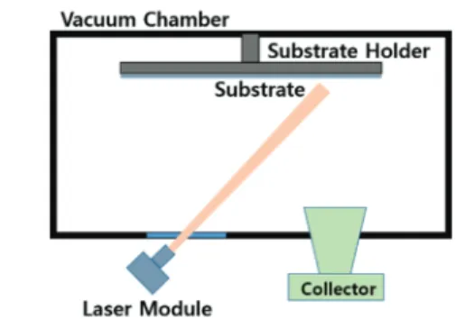
2.2 Electrical Contact Method using Laser Fig. 1 is a systematic diagram of high vacuum system for making electrical contacts between anode auxiliary electrode and thin cathode after eliminating EL layers by laser module. When the substrate for forming electrical contact between the thin cathode and the anode auxiliary electrode is transferred to the vacuum chamber, the substrate is fixed on top of the vacuum chamber. The bottom of the vacuum chamber is equipped with a laser module to remove the deposited EL layer on the anode auxiliary electrode. The
laser beam irradiated from the laser module is incident into the vacuum chamber through a transparent window installed under the vacuum chamber and is precisely aligned on the anode auxiliary electrode. After aligning exactly like this, it starts to selectively etch EL materials in a desired area, and then makes contacts with the anode auxiliary electrode according to the cathode deposition in a subsequent process, thereby enabling Voltage Drop compensation.
Fig. 1. The system diagram of high vacuum system for contacting anode auxiliary electrode and thin cathode after eliminating EL layers by laser module.
In addition, a particle collector is installed under the vacuum chamber to remove fine hume-like particles that may occur during the process. Also, another important point could be a process pressure of laser removal. In order to minimize the characteristic change of the multi-layered EL, which is a self-luminous current driving method, the process of removing the EL layer on the anode auxiliary electrode using this laser has a high vacuum of 10
-5Pa or more similar to the deposition conditions of EL materials. This series of systems can be fully optimized for the elimination of EL materials on the anode auxiliary electrode via laser and for the Voltage Drop compensation through these electrical contact with the cathode to the anode auxiliary electrode.
2.3 Absorption Coefficient of EL materials according to Laser Wavelength
In order to effectively and clearly remove the EL layers
on the anode auxiliary electrode by the laser module
mentioned in Fig. 1, the absorption coefficient according to
the laser wavelength of the EL material, which is an organic
material, should be investigated first to find the wavelength
range where the laser can absorb the EL material best. This
Recent Progress on Voltage Drop Compensation in Top Emission Organic Light Emitting Diodes (OLED) 51
allows the EL layer deposited on the anode auxiliary electrode to be completely removed and a stable electrical contact with the cathode material deposited in subsequent process.
Fig. 2 shows the absorption spectra of the organic materials according to the wavelength [15]. It can be seen that the absorption coefficient increases most significantly below 355nm of wavelength of laser. Based on these results, various laser wavelength bands, such as 355nm and 266nm, were selected and the removal ability of the deposited EL multiple layers was evaluated.
In the condition of 355nm of laser wavelength, the selectivity for the anode auxiliary electrode was the best.
Excimer lasers with less than 300nm were excluded from this study due to damage to the underlying metal film. (not shown in this paper)
Fig. 2. The absorption spectra of the organic materials according to the wavelength [15].
3. Result & Discussion 3.1 Anode Auxiliary Electrode Design for
Voltage Drop Compensation
In order to optimally compensate for the Voltage Drop at the center and the edge of the panel due to the thin cathode in the large-area top-emission OLED and to maximize the aperture ratio in the substrate, it is necessary to minimize and efficiently arrange the size of the anode auxiliary electrode contacted with the thin cathode. Therefore, anode auxiliary electrode was designed for every pixel in the position adjacent to R, G, and B pixels, as shown in Fig. 3.
Auxiliary electrodes were placed directly adjacent to every pixel and the anode auxiliary electrode is patterned at the
same time when the anode pixel electrode is formed. After that, a PDL (pixel define layer) is formed on the anode auxiliary electrode, and then multi-layered EL layers such as PHIL, HTL, EML, and ETL are deposited in order.
However, the gap between anode auxiliary electrodes contacting cathode was optimized to minimize the process time in consideration of the simulation results and the luminance non-uniformity of the panel, based on the circuit diagram as shown in Fig. 4. In other words, it is not necessary to form an electrical contact on the anode auxiliary electrode existing for every pixel to secure a mass production process time, and the electrical contact on the auxiliary electrode is formed by laser at pixel intervals optimized for the resolution of each substrate.
Fig. 3. The systematic drawing of in-panel array of anode auxiliary electrode in top emission OLED panel.
Fig. 4. The circuit diagram showing electrical contacts between thin cathode and an anode auxiliary electrode.
3.2 The Sequential Process of Electrical Contact
Fig. 5 is a process sequence detailing the electrical contact
between the anode auxiliary electrode and the thin cathode
using a laser. When the entire EL multi-layer is removed
Byoung-Seong Jeong 52
using a 355nm laser and the cathode is deposited in a subsequent process, the anode auxiliary electrode and the cathode layer are electrically connected to each other, and the Voltage Drop through the thin cathode can be compensated. If the multiple EL layers are not completely removed, residues of the EL films exist between the anode auxiliary electrode and the thin cathode. These residues do not provide good electrical contact between the cathode and anode auxiliary electrodes, so they need to be overetched sufficiently to remove them completely.
Fig. 5. The multi-layered EL removal process sequence using laser.
3.3 The Applied Result of 355nm Laser
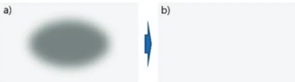
Fig. 6 is an optical micrograph of the contact hole by 355nm laser after removing the multi-layered EL layer formed on the anode auxiliary electrode [16]. As shown in the Fig. 6, when the organic material was irradiated with laser, a circular contact hole was formed. In the area outside the contact point, blur-like phenomena are observed. This blur occurs when the high-temperature laser is incident, due to the volume expansion caused by rapid temperature rise and shrinkage by rapid temperature down. However, since the blur hill is formed smoothly in cross-section analysis, disconnection is not generated by the metal-based cathode which is subsequently deposited. Thus, there is no problem in the voltage supply through the electrical connection to the anode auxiliary electrode with thin cathode.
Fig. 6. The top-view micro-structure of contact hole after EL layer removal using 355nm laser [16].
3.4 The Consideration of Contact Hole Size The contact hole size applied in this study is 25 5m in diameter. Generally, it can be applied to lower than 25m.
However, the contact size was not reduced to the minimum size in order to improve the process completion. In addition, in order to reduce the process time, as shown in Fig. 7, the number of laser heads was increased to construct a multi- laser head system. The system allows the substrate to move and simultaneously remove EL material on the anode auxiliary electrode on a large substrate with just one scan.
Therefore, there is no additional process time loss due to the formation of numerous laser contacts.
Fig. 7. The schematic diagram of laser contact process with multi-laser head.
3.5 Improvement of Luminance Uniformity through Laser Contact Method
Fig. 8 compares luminance uniformity before and after Voltage Drop compensation through laser contact. For accurate measurement of uniformity, 9 points per panel was measured and calculated as Luminance Uniformity (%) = (max.- min) / (max. + min.), where max. stands for maximum luminance and min. stands for minimum luminance. Before applying the laser contact method, as shown in 8(a), the voltage lead-in part outside the panel has high brightness while the brightness gets lower toward the center of the panel. The long range uniformity (LRU) of 9 points in the panel is about 15%.
However, it was found that the luminance uniformity,
which compensated the Voltage Drop for the thin cathode
through the anode auxiliary electrode, was improved by
more than 80% using the laser contact method. In addition,
there was no dark spot or dark pixel due to the electrical
Recent Progress on Voltage Drop Compensation in Top Emission Organic Light Emitting Diodes (OLED) 53
short between the anode and the cathode at the top of the pixel located near the anode auxiliary electrode due to particles that could occur during the laser process, which was considered as a risk of the laser contact method.
Therefore, a new method of compensating for Voltage Drop by contacting the anode auxiliary electrode and the thin cathode by using such a laser is expected to become a necessary process in the future in the large size top emission OLED panels.
Fig. 8. The improvement of luminance uniformity through laser contact method. a) before Voltage Drop compensation. b) after Voltage Drop compensation through laser contact.
4. Conclusion
The Voltage Drop due to the thin cathode in the top emission method that can maximize the aperture ratio in large size OLED was successfully compensated by removing the EL layer deposited on the anode auxiliary electrode using 355nm laser and then making electrical contacts with depositing thin cathode to the anode auxiliary electrode in the subsequent process. It was found that the luminance uniformity dramatically increased through this electrical compensation. The EL removal method using laser in such a large size top emission OLED is considered to be a useful process for high resolution top emission OLED panels requiring long life.
References
1. Tsujimura, T., OLED Display Fundamentals and Applications, New Jersey: John Wiley & Sons, 2017.
2. Oh, C.-H., Shin, H.-J., Nam, W.-J., Ahn, B.-C., Cha, S.- Y., Yeo, S.-D., “Technological Progress and Com- mercialization of OLED TV,” SID Digest, pp. 239-242, 2013.
3. Lee, W.J., “Study on the Electrical Conduction Me- chanism of Organic Light-Emitting Diodes (OLEDs),”
Journal of the Semiconductor & Display Technology,
17(4), pp.6-11, 2018.
4. Sekitani, T., Nakajima, H., Maeda, H., Fukushima, T., Aida, T., Hata, K., Someya, T., “Stretchable Active- Matrix Organic Light-Emitting Diode Display using Printable Elastic Conductors,” Nature Materials 8, pp.
494-499, 2009.
5. Yin, D., Feng, J., Ma, R., Liu, Y.-F., Zhang, Y.-L., Zhang, X.-L., Bi, Y.-G., Chen, Q.-D., Sun, H.-B, “Efficient and Mechanically Robust Stretchable Organic Light- Emitting Devices by a Laser-programmable Buckling Process,” Nature Communications, pp. 1-7, 2016.
6. Han, C.-W., Han, M.-Y., Joung, S.-R., Park, J.-S., Jung, Y.-K., Lee, J.-M., Choi, H.-S., Cho, G.-J., Kim, D.-H., Yee, M.-K., Kim, H.-G., Choi, H.-C., Oh, C.-H., Kang, I.-B., “3 Stack-3 Color White OLEDs for 4K Premium OLED TV,” SID Digest, pp. 1-4, 2017.
7. Tani, R., Yoon, J.-S., Yun, S.-I., Nam, W.-J., Takasugi, S., Kim, J.-M., Park, J.-K., Kwon, S.-Y., Kim, P.-Y., Oh, C.- H., Ahn, B.-C., “Panel and Circuit Designs for the World’s First 65-inch UHD OLED TV,” SID Digest, pp.
950-953, 2015.
8. Chen., S., Deng, L., Xie, J., Peng, L., Xie, L., Fan, Q., Huang, W., “Recent Developments in Top-Emitting Organic Light-Emitting Diodes,” Advanced Materials, pp. 5227-5239, 2010.
9. Moon, J.I., Cho, S.J., Cho, E.S., Nam, C., Kwon, S.J.,
“Bandgap Voltage Reference Circuit Design Technology Suitable for Driving Large OLED Display Panel,”
Journal of the Semiconductor & Display Technology, 17(2), pp.53-56, 2018.
10. Han, S., Feng, X., Lu, Z.H., Johnson, D., Wood, R.,
“Transparent-Cathode for Top-Emission Organic Light- Emitting Diodes,” Applied Physics Letters, pp. 2715- 2717, 2003.
11. Mertens, R., Sony’s Super Top Emission technology explained, https://www.oled-info.com/sonys-super-top- emission-technology-explained, 2013.
12. Wei, M.-K., Lin, C.-W., Yang, C.-C., Kiang, Y.-W., Lee, J.-H., Lin, H.-Y., “Emission Characteristics of Organic Light-Emitting Diodes and Organic Thin-Films with Planar and Corrugated Structures,” Int. J. of Molecular Sciences, pp. 1527-1545, 2010.
13. Hwang, C.H, Kim, S.S., Bang, S.W., Choi, S.H., Chin, B.D., Jo, S.M., Lee, J.Y., “Review of Vacuum Thermal Evaporation for Future AMOLED,” The World of Physics and Advanced Technology, pp. 29-37, 2018.
14. Lee, S.Y, Koo, H., Cho, S.H., “Mask-less Patterning of
Organic Light Emitting Diodes using Electrospray and
Byoung-Seong Jeong 54
![Fig. 6. The top-view micro-structure of contact hole after EL layer removal using 355nm laser [16]](https://thumb-ap.123doks.com/thumbv2/123dokinfo/4722905.510055/4.825.166.329.778.947/fig-micro-structure-contact-layer-removal-using-laser.webp)