P1-69 / C. W. Joo
• IMID 2009 DIGEST Abstract
High efficiency white organic light emitting diodes were fabricated by using an alignment free mask patterning method. Only red/green emission without any blue emission was observed in the red/green patterned region and blue emission was emitted in other area. A combination of the red/green and blue emission gave a high efficiency white emission. A maximum current efficiency of 30.7 cd/A and a current efficiency of 25.9 cd/A at
1000 cd/m2 were obtained with a color coordinate
of (0.38, 0.45).
1. Introduction
White organic light-emitting diodes (WOLEDs) have been developed for applications as a display and general lighting and there have been much progress in device performances. They have many advantages over other displays or light sources such as flexibility, design freedom, thin and light, distributed light emission, and low cost manufacturing.
The most important performance of WOLEDs is light-emitting efficiency, and most researches were focused on improving the quantum efficiency of WOLEDs [1]. WOLEDs can be fabricated by using a stacked emitting layer structure, a single layer emitting structure. The stacked emitting layer structure can be realized by using red/green/blue(RGB) or red/blue(RB) stacked emitting layers. The stacked emitting layer structure has a merit of high efficiency in spite of poor color stability. Compared with the stacked WOLED structure, the single layer structure has only one emitting layer doped with red/green/blue or red/blue dopant materials. Even though the emitting structure
is simple, it is difficult to get high efficiency and good color stability. The color converting structure is simple to realize, but the efficiency of the blue emitting layer should be high to gethigh efficiency from the device[2]. Other than the stacked and single layer mixed structure, a color converting structure has also been developed to get white emission using single emitting layer and color converting materials [3].
In this work, we developed a new simple device fabrication for method for white organic light-emitting diodes which can achieve high efficiency and color stability. The blue emitting layer was stacked on fine metal mask patterned red/green emitting layer in some area and it will exist as a blue single layer in the area without red/green layer. The blue layer can play a role of hole blocking layer of the red/green emitting layer. It was demonstrated that the alignment free mask patterning method is effective to fabricate high efficiency WOLEDs.
2. Experimental
Three different devices were fabricated to study effect of patterning on device performances of WOLEDs. Red emitting layer had a stack structure indium tin oxide(ITO, 150 nm)/poly-3,4-ethylene-dioxy-thiophene:polystyrenesulfonate (PEDOT:PSS, 60 nm)/ N, N'-di(1-naphthyl)-N,N'-diphenylbenzidine-(NPB, 10 nm)/ 4,4',4"-tris(N-carbazolyl)tripheny-lamine(TCTA, 10 nm)/N, N'-dicarbazolyl-3,5-benzene(mCP,10 nm)/TCTA:3-phenyl-4-(1'-naphthyl)-5-phenyl-1,2,4-triazole(TAZ): iridium(III) tris(2-phenylpyridine)(Ir(ppy)3):iridium(III) bis(1-phenylquinoline) acetylacetonate(Ir(pq)2-acac)(20 nm, 10%, 1%)/2-diphenylphosphorylspirofluorene-(SPPO1): iridium(III) bis(4,6-(di-fluorophenyl)-Development of an alignment free mask patterning as a new
fabrication method for high efficiency white organic light-emitting diodes
Chul Woong Joo, Soon Ok Jeon, Kyoung Soo Yook, Jun Yeob Lee* Dept. of Polymer Science and Engineering, Dankook University Jukjeon-dong, Suji-gu, Yongin-si, Gyounggi-do, 448-701, Korea
P1-69 / C. W. Joo
IMID 2009 DIGEST •
pyridinato-N,C2') picolinate (FIrpic) (30 nm, 15%)/4,7-diphenyl-1,10-phenanthroline(Bphen, 5 nm)/tris(8-hydroxy-quinoline)aluminum(Alq3, 20 nm)/LiF(1 nm)/Al(200 nm). Blue emitting layer had a stack structure of (ITO, 150 nm)/(PEDOT:PSS, 60 nm)/ (NPB, 10 nm)/(TCTA, 10 nm)/(mCP,10 nm)/ SPPO1: FIrpic(30 nm, 15%)/ Bphen(5 nm)/ Alq3(20 nm)/LiF(1 nm)/Al(200 nm). Pixel size was 2 mm by 2 mm and the open width of stripe type metal mask was controlled to investigate the effect of the emitting area of red/green and blue colors on the device performances of pixel divided white devices. Current density–voltage–luminance characteristics and electroluminescence (EL) spectra of PHOLEDs were measured with Keithley 2400 source measurement unit and CS 1000 spectrophotometer.
3. Results and discussion
It is required to use hole blocking type blue phosphorescent emitting layer to get high efficiency and pure red/green emission in red/green emitting layer. Therefore, a new electron transport type blue phosphorescent host material based on spirofluorene and phosphine oxide was synthesized. The 2-(diphenylphosphoryl)spirofluorene(SPPO1) had a triplet bandgap of 2.8eV and the highest occupied molecular orbital(HOMO) level of 6.5eV. Therefore, SPPO1 layer can play a role of hole blocking layer on red/green emitting layer.
Figure 1. Schematic diagram of the white organic light-emitting diodes with divided pixel area for red/green and blue emission.
The device structure of the patterned WOLEDs and schematic diagram of the pixel structure is shown in Fig. 1. The relative area of the red/green emitting region was 50% in patterned WOLEDs
Figure 2. Current density-voltage curves of Red/Green, Blue and White device Luminance-voltage curves (inset : Luminance-Luminance-voltage curve)
Fig. 2. shows the current density-voltage curves of red/green, blue and white devices. The current density was high in the blue device, while red/green device showed the lowest current density because of the thickness of the emitting layer as shown in Fig. 2. Total thickness of the emitting layer in the red/green device was 50 nm compared with 30 nm of the blue device, resulting in low current density in the red/green device. Luminance of the three devices followed the same trend as the current density because the luminance is mostly affected by charge density in the emitting layer.
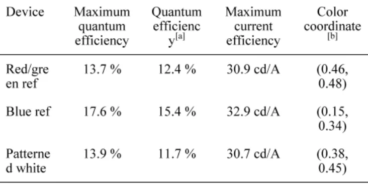
Table 1. Device performances of the red/green, blue
and white devices
Device Maximum quantum efficiency Quantum efficienc y[a] Maximum current efficiency Color coordinate[b] Red/gre en ref 13.7 % 12.4 % 30.9 cd/A (0.46, 0.48)
Blue ref 17.6 % 15.4 % 32.9 cd/A (0.15,
0.34) Patterne
d white 13.9 % 11.7 % 30.7 cd/A (0.38, 0.45)
[a] Quantum efficiency was measured at 1000 cd/m2
[b] Color coordinate was measured at 1000 cd/m2
Quantum efficiency of the red/green, blue and white devices are shown in Fig. 3. The red/green device with blue emitting layer stacked on red/green emitting layer showed a quantum efficiency of 11.7% and a current efficiency of 25.9 cd/A at 1000 cd/m2 And
P1-69 / C. W. Joo
• IMID 2009 DIGEST
The blue standard device showed a quantum efficiency of 13% and a current efficiency of 29 cd/A at 1000 cd/m2. The white device showed a little lower quantum efficiency value than red/ green and blue devices. A maximum current efficiency of 30.7 cd/A and a current efficiency of 26.6 cd/A at 1000 cd/m2 were achieved in the white device.
Figure 3. Electroluminescence spectra of red/green, blue and White devices.
To confirm the separate emission of the red/green and blue colors, the EL spectra of the red, blue and WOLED were measured.Fig.3 Compares EL spectra of red/green, blue and white devices. The red/green device showed a red/green emission with little blue emission from the blue emitting layer stacked on the red/green emitting layer. This indicates that most excitons are generated inside the red/green emitting layer and the blue emitting layer does not contribute to the red/green light emission. The white device showed emissions from the red/green emitting region and blue region. Therefore, the area divided pixel structure was effective to get white emission.
4. Summary
High efficiency WOLEDs could be easily fabricated by a new alignment free mask pattering method. The new patterning method is advantageous because red/green and blue emission could be controlled separately. A maximum current efficiency of 30.7 cd/A was obtained and there was no charge leakage between emitting layers. Highly efficient and color stable in WOLEDs could be simply realized
using our new fabricated method. The alignment free mask patterning method is expected to be useful as a new fabrication method of WOLEDs.
Acknowledgement
This work partially supported by the GRRC program of Gyeonggi province [GRRC Dankook 2009-B01, Materials development for high efficiency organic solid state lighting], grant No. RTI04-01-02 from the Regional Technology Innovation Program of the Ministry of Knowledge Economy (MKE), MKE/ITEP [10028439-2008-21], and a grant (M2009010025) from the Fundamental R&D Program for Core Technology of Materials funded by the MKE.
5. References
1. Y. Sun, N.C. Giebink, H. Kanno, B.W. Ma, M.E. Thompson, S.R. Forrest, Nature 440 (2006) 908. 2. G. Tu, Q. Zhou, Y. Cheng, L.X. Wang, D.G. Ma, F.S.
Wang, Appl. Phys. Lett. 85 (2004) 2172.
3. J.Y. Lee, J.H. Kwon, H.K. Chung, Org. Electron. 4 (2003) 14.