1. 서 론
전력 반도체 소자는 1 W 이상의 전력을 제어할 수 있는 능력을 가진 반도체이다. 전력용 반도체는 크게 MOSFET (metal oxide semiconductor field effect transistor)과 IGBT (insulated gate bipolar transistor) 로 나뉘는데 MOSFET은 캐리어라 부르는 electron 또 는 hole을 이용하여 빠른 스위칭 속도를 보여주지만
✉ Ey Goo Kang; [email protected]
Copyright ©2019 KIEEME. All rights reserved.
This is an Open-Access article distributed under the terms of the Creative Commons Attribution Non-Commercial License (http://creativecommons.org/licenses/by-nc/3.0) which permits unrestricted non-commercial use, distribution, and reproduction in any medium, provided the original work is properly cited.
항복전압을 높이거나 전류량을 높이는 데 한계가 있다.
하지만 IGBT는 주로 600 V 이상의 전압 영역에서 널 리 사용되고 있으며, 고효율, 고속의 전력 시스템에 특 히 많이 사용되고 있다 [1-4].
본 논문에서는 trench gate 밑에 존재하고 있는 전 계 집중에 따라 항복전압 특성의 변화를 확인하기 위 하여 실험(simulation)을 진행하였으며, gate 밑에 P- 영역의 크기에 따른 실험과 trench gate와 trench gate 사이에 영역(이하 N+ Drift)에 변화에 따른 실험 후 전기적 특성인 문턱 전압, 온-상태 전압 강하 및 항복전압 등의 특성을 분석하였다 [5,6].
실험은 Synopsys사에 T-CAD 툴을 활용하여 해당 소자의 시뮬레이션을 통해 검증하였다.
Trench Gate 하단 P-영역을 갖는 IGBT의 전기적 특성에 관한 연구
안병섭1, 육진경2, 강이구1,2
1 극동대학교 에너지IT공학과
2 극동대학교 교양학과
Study on Electric Characteristics of IGBT Having P Region Under Trench Gate
Byoung Sub Ann
1, Jinkeoung Yuek
2, and Ey Goo Kang
1,21 Department of Energy IT Engineering, Far East University, Uem-sung 27601, Korea
2 Department of General Education, Far East University, Uem-sung 27601, Korea
(Received March 22, 2019; Revised April 25, 2019; Accepted May 7, 2019)
Abstract: Although there is no strict definition of a power semiconductor device, a general description is a semiconductor that has capability to control more than 1 W of electricity. Integrated gate bipolar transistors (IGBTs), which are power semiconductors, are widely used in voltage ranges above 300 V and are especially popular in high-efficiency, high-speed power systems. In this paper, the size of the gate was adjusted to test the variation in the yield voltage characteristics by measuring the electric field concentration under the trench gate. After the experiment Synopsys’ TCAD was used to analyze the efficiency of threshold voltage, on-state voltage drop, and breakdown voltage by measuring the P- region and its size under the gate.
Keywords: Trench gate, IGBT, Vth, BV, Vce-sat
ISSN 1226-7945(Print), 2288-3258(Online)
2. 실험 방법
2.1 Trench gate IGBT 기본구조
이번 실험에서 사용할 trench gate type field stop IGBT의 구조는 그림 1과 같으며 1,200 V급의 파라미 터는 표 1에 표기했다.
Fig. 1. Trench gate type field stop IGBT.
Classification Unit Value
Cell pitch ㎛ 3
Gate pitch ㎛ 1
P-base pitch ㎛ 2
N+emitter pitch ㎛ 0.3
N+emitter dose cm3 4.5E19
P+emitter dose cm3 1.7E19
P-base emitter dose cm3 2.0E13
Total cell depth ㎛ 130
P+emitter depth ㎛ 0.3
P-base depth ㎛ 1
P+collector depth ㎛ 0.5
F-S layer depth ㎛ 5
F-S layer dose cm3 1.0e16
N-drift (resistivity) Ω/cm 70
Table 1. Trench gate type SUP field stop IGBT paramater.
2.2 트렌치 게이트 하단 P 영역의 깊이에 따른 실험 이 실험은 trench gate의 depth를 6 ㎛까지 boron 을 주입하고 1 ㎛를 더 식각하여 gate 수직 부분에 boron implant된 영역까지 제거하여 P-layer를 형성 하였고, P-layer의 크기에 따라 Vth, BV, VCE-SAT 의 값을 확인하였다.
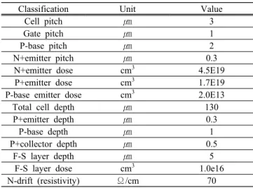
2.2.1 P-layer distance에 따른 electric field 실험은 그림 2에서 보는 것과 같이 P-layer depth 가 0~1 ㎛까지 변화에 따라 electric field 분포에 대 해 분석하였다.
측정 부분은 그림 3에서 보는 것과 같이 trench gate 아래 P-layer (a) 부분(이하 P-layer) (line A)과 gate를 지나지 않는 collector와 emitter 직선상 P-base (b)와 N-drift (c) 부분(이하 P-base layer) (line B)의 electric field를 측정하였다.
Fig. 2. The variation of the depth P-layer distance.
Fig. 3. Electric field measurements.
2.2.2 P-영역의 및 N+ 드리프트 영역의 dose에 따른 실험
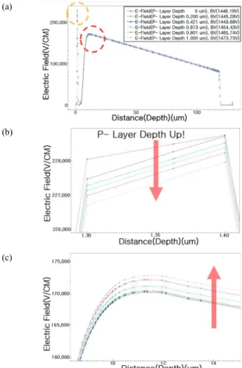
다음 실험은 그림 4에서 보는 것과 같이 P-layer의 크기를 1 ㎛로 고정한 후에 P-layer의 implant dose 를 1e10~1e14 cm-2, N+ Drift Dose를 4e13~7e13 cm-2까지 변화를 주어 실험을 진행하였고, 그 결과를 3장에 나타냈다.
3. 결과 및 고찰
3.1 P-영역 깊이에 따른 실험 결과
표 2와 그림 5는 실험 2.2.1에서 실험한 것을 나타 내였다. P-영역의 깊이의 변화에 따라 온-상태 전압강 하 특성은 오차범위 안에서 큰 영향이 없었지만, 깊이 가 0.4 ㎛ 이상부터 항복전압 특성이 상승하는 것을 확인할 수 있었다.
이에 따른 실험 결과로 그림 6, 7은 전계 특성을 보
Fig. 5. According to P-layer distance BV (V), VCE-SAT (V).
P layer depth (㎛) Vth (V) BV (V) VCE-SAT (V)
0.000 4.57676 1446.19 1.00678
0.200 4.14894 1445.28 1.01290
0.313 4.14894 1444.25 1.01120
0.421 4.14894 1443.68 1.01303
0.506 4.14894 1448.08 1.01156
0.613 4.14894 1454.44 1.00728
0.717 4.14894 1461.62 1.00697
0.801 4.14894 1465.74 1.00557
0.903 4.14894 1470.29 1.00916
1.000 4.14894 1473.73 1.00601
Table 2. The experiment according to P-layer distance under the gate bottom.
Fig. 4. N+ drift and P-layer dose the doping concentration (cm-3).
(a)
(b)
Fig. 6. Line A of electric field according to P-layer.
(a)
(b)
(c)
Fig. 7. Line B of electric field according to P-layer.
여주고 있다. 그림 6(a)는 그림 3의 line A에 전계 특 성이며 그림 6(b)는 그림 6(a)의 점선 원을 확대한 그 림으로 P-layer depth (um)가 증가할수록 전계집중이 줄어들었다.
또한 그림 7(a)는 그림 3의 line B에 전계 특성이며 그림 7(b)는 그림 7(a)의 P-Base영역을 확대한 전계특 성이고, 그림 7(c)는 그림 7(a)의 N-Drift를 확대한 전 계특성으로 P-layer depth (um)가 증가할수록 높았던 영역(P-Base) 은 낮아지고, 낮았던 영역(N-Drift)은 높 아져 전체적인 전계특성이 고르게 향상되었다.
3.2 P-영역 및 N+ 드리프트 영역의 dose에 따른 실험 결과
실험 2.2.2에 결과는 그림 8과 같이 N+ drift dose 는 농도가 높아질수록 항복전압은 낮아지지만, 온-상
태 전압강하 특성은 좋아지는 것을 확인할 수 있다.
그림 8(c)에서 보는 것과 같이 P-layer의 implant dose가 5e11~2.25e12 cm-2까지 점차 항복전압이 상 승하는 것을 확인할 수 있었지만 그 이상이 되면 항복 전압이 급격하게 떨어지는 것을 확인할 수 있다.
문턱전압 특성(그림 8(b))에서 보는 것과 같이 N+
drift의 농도에 따라서 문턱전압은 내려가고 이와 반대 로 P-layer의 농도가 1e13 cm-2 이상이 되면 문턱전 압 특성이 다시 상승하는 것을 확인할 수 있다.
4. 결 론
본 실험을 통하여 게이트 하단 부분에 P-layer에 유 무에 전계 특성에 변화를 확인하였고, 전기적인 특성이 변화하는 것을 확인할 수 있었다. P-layer에 크기 및 농도에 따라 전기적인 특성이 좋아지는 것을 확인되었 으며, trench gate 사이에 영역에 변화에 따라 전기적 특성을 분석하였다. 본 구조에 의해 다양한 항복전압을 갖는 IGBT를 구현할 것으로 판단되며, 향후, 신재생에 너지 및 전기자동차에 응용 가능할 것으로 사료된다.
ORCID
Ey Goo Kang https://orcid.org/0000-0001-7600-7303
감사의 글
본 연구는 한국에너지평가기술원의 2019년 선정 2단 계 에너지인력양성사업(20194010201810)과 한국전력공 사의 2017년 선정 기초연구개발 과제 연구비에 의해 지원되었음(과제번호: R17XA05-59).
REFERENCES
[1] E. G. Kang, B. S. Ahn, and T. J. Nam, J. Korean Inst. Electr.
Electron. Mater. Eng., 23, 273 (2010). [DOI: https://doi.org/
10.4313/JKEM.2010.23.4.273]
[2] Y. S. Cho, E. S. Jung, K. M. Oh, and M. Y. Sung, J. Korean Inst.
Electr. Electron. Mater. Eng., 25, 247 (2012). [DOI:
https://doi.org/10.4313/JKEM.2012.25.4.247]
[3] J. S. Lee, E. G. Kang, and M. Y. Sung, J. Korean Inst. Electr.
Electron. Mater. Eng., 19, 912 (2006). [DOI: https://doi.org/
(a)
(b)
(c)
Fig. 8. The characteristic of P-layer and N+ driver area dose according to Vth (V), BV (V), VCE-SAT (V).
10.4313/JKEM.2006.19.10.912]
[4] E. G. Kang, J. Korean Inst. Electr. Electron. Mater. Eng., 29, 681 (2016). [DOI:https://doi.org/10.4313/JKEM.2016.29.11.681]
[5] B. S. Ann and E. G. Kang, Journal of IKEEE, 22, 339 (2018).
[DOI: https://doi.org/10.7471/ikeee.2018.22.2.339]
[6] J. M. Geum, E. S. Jung, E. G. Kang, and M. Y. Sung, J. Korean Inst. Electr. Electron. Mater. Eng., 25, 253 (2012). [DOI:
https://doi.org/10.4313/JKEM.2012.25.4.253]