Voltage Island Partitioning Based Floorplanning Algorithm
Jaehwan Kim*, Jong-Wha Chong*★
Abstract
As more and more cores are integrated on a single chip, power consumption has become an important problem in system-on-a-chip (SoC) design. Multiple supply voltage (MSV) design is one of popular solutions to reduce power consumption. We propose a new method that determines voltage level of cores before floorplanning stage.
Besides, our algorithm includes a new approach to optimize wire length and the number of level shifters without any significant decrease of power saving. In simulation, we achieved 40-52% power saving and a considerable improvement in runtime, whereas an increase in wire length and area is less than 8%.
Keywords: Floorplan, low power, voltage island, VLSI
* Dept. of Electronics and Computer Engineering, Hanyang University
★Corresponding author
※ Acknowledgement
This work was sponsored by ETRI SW-SoC R&BD Center, Human Resource Development Project. This research was also supported by the MKE (The Ministry of Knowledge Economy), Korea, under the ITRC(Information Technology Research Center) support program supervised by the NIPA(National IT Industry Promotion Agency) (NIPA-2012-H0301-12-1011). The IDEC provide research facilities for this study.
Manuscript received Aug.8.2012,; revised Aug.20.2012 I. Introduction
In recent years, reduction of power consumption is an important issue in system-on-a-chip (SoC) design because more and more IP cores are integrated on a single chip and the power density is increased. Power consumption is mostly divided into static power and dynamic power, and the dynamic power is proportional to the square of the supply voltage. Therefore, multiple supply voltage (MSV) designs lowering the supply voltage of each core are widely used to reduce power consumption.
In MSV floorplanning step, each core is assigned to a specific voltage level, and contiguous cores
with same voltage level are partitioned into same group called voltage islands. These voltage islands enable different voltages to be supplied to different areas on a chip, whereas it makes design complexity more complicated. For example, a level shifter which causes additional power consumption and area has to be inserted to interconnect from a low voltage core to a high voltage core. Moreover, power network complexity also has to be considered.
There are several previous papers addressing MSV floorplanning. A common goal of these papers is to optimize area, wire length and power consumption simultaneously. Mak and Chen in [1] generated a few candidate floorplan solutions based on area and wire length. Then voltage island partitioning that determines the voltage level of cores was implemented to find the best solution between them using ILP. Ma and Young in [2] proposed voltage island partitioning algorithm performed during floorplaning. Whenever cores are moved, voltage island partitioning is performed. However, there is a weakness in previous works. The rest voltage island partitioning steps except for the best case are not used and eventually waste a lot of time [3].
In our work, we propose a new voltage assignment
Core name C1 … Cm Voltage level
(V) 1.1 1.3 1.8 … 1.5 1.8
Power consumption
(W)
10.89 15.21 29.16 … 15.75 22.68 algorithm for short runtime. In order to avoid repeating voltage assignment to cores in floorplan stage, it is implemented only once before floorplanning. Besides, previous papers minimize power consumption without any significant increase in area and wire length. On the other hand, we suggest a new approach which tries to minimize wire length and the number of level shifters while total power consumption stays in a proper range.
The rest of this paper is organized as follows. In section 2, we formulate our problem. In section 3, we propose our methodology for MSV floorplanning.
Simulation results are discussed in section 4, and conclusion is provided in section 5.
II. Problem Formulation
Our MSV floorplanning consists of 2 steps, voltage assignment and power network-aware floorplanning.
In the first step, voltage assignment problem, we are given a set of cores and a netlist of cores. Each core has a power table that includes the legal voltage levels of the core and the corresponding power consumption as shown in table 1. We assume that the legal voltage levels of each core are determined independently regardless of other cores like [1], [2], [3] and [4]. Our goal of this step is to decide the proper voltage level for each core.
Table 1. POWER TABLE OF CORE
Second step is power network-aware floorplanning.
In this step, given the voltage level of each core, the position of the cores are determined such that area, wire length and power network complexity are considered at the same time. A lot of voltage islands make design complicated during floorplanning. Therefore, we assume that the number of voltage islands equals to the number of legal voltage level for all cores.
Ⅲ. MSV Floorplanning Algorithm
A. Voltage Assignment
In voltage assignment problem, our goal is to decide the voltage level of cores such that total power saving, total wire length and the number of level shifters are optimized at the same time. Power consumption is determined by the voltage level of cores, and the number of level shifters is calculated by the number of interconnects from the low voltage core to the high voltage core. However, it’s difficult to compute total wire length precisely because the position of cores is not determined before floorplanning. Therefore, we predict wire length through the number of interconnects. If a core had a lot of interconnects with other cores in the same voltage island, wire length would be small, because cores are contiguous when they are in the same voltage island. On the other hand, if a core had a lot of nets with other cores in the other voltage islands, wire length would be long.
We define notations used in this problem below.
Ø c represents core, we suppose that the total number of cores is m (1 ≤ c ≤ m).
Ø NVc indicates the number of legal voltage levels of core c (1 ≤ c ≤ m).
Ø Core c has a set of legal voltages {Vc(1), Vc(2), . . . , Vc(NVc)} where Vc(k) is the voltage of core c when it operates at voltage level k (1 ≤ c ≤ m, 1 ≤ k ≤ NVc).
Ø Core c has a set of power consumption {Pc(1), Pc(2), . . . , Pc(NVc)} where Pc(k) is the power consumption of core c when it operates at voltage level k (1 ≤ c ≤ m, 1 ≤ k ≤ NVc).
Ø Core c has a set c.setN { Nc(1), Nc(2), . . . , Nc(NVc)} where Nc(k) is the number of interconnect between core c and other cores operated at voltage levelk (1 ≤c ≤m, 1 ≤k ≤NVc).
Ø c.CVI represents the current voltage level of core c, and c.NVI represents the next voltage level of core c when its voltage level is
changed.
Ø c.cost represents the cost value of core c.
Ø MIN_PC denotes the minimum total power consumption. In other words, MIN_PC is the power consumption when all cores are assigned to their lowest possible voltage level.
Ø MAX_PC denotes the maximum total power consumption. It’s the upper bound of CUR_PC and a constant which is defined by user.
Besides, MAX_PC is similar power consumption that we want to get in a final solution.
Ø CUR_PC denotes the current total power consumption.
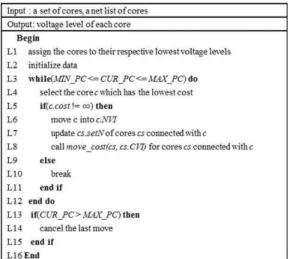
An outline of voltage assignment step is presented in Fig. 1. In this step, the voltage level of cores is changed to improve wire length and the number of level shifters while CUR_PC is increased from MIN_PC to MAX_PC. However, increase of power consumption is not a problem because MAX_PC still causes significant power saving. In other words, our power consumption without any significant increase in wire length.
Fig. 1. Outline of Voltage Assignment
Voltage assignment algorithm is implemented as follows. First, cores are assigned to their respective lowest voltage levels such that total power
consumption is minimized because there isn’t a big difference between the lowest possible total power consumption and the final total power consumption in recent papers. Moreover, small scope of possible power consumption makes runtime short [L1]. Next, data like MIN_PC and c.setN are initialized. For instance, MIN_PC is assigned by initial value of CUR_PC [L2]. Then, the process that changes voltage level of each core is repeated until CUR_PC is larger than MAX_PC. Only one core is moved into its other voltage island at one repetition, and the core with the lowest cost is chosen to move.
The cost value of the core means variation of power consumption when the voltage level of the core is changed with consideration for wire length, the number of level shifters and power saving, and the cost value ∞ of the core means that the core does not need to change its voltage level. In L5-L8, because the cost of core c that is picked up to move is not ∞, c is moved into its other legal voltage island, and function move_cost() is called to update values of cost and NVI modified by a change of setN of cores connected with c. In L9-L11, iteration is terminated because there are not any cores to move into other voltage islands any more. In L13-L15, it prevents CUR_PC from being larger than MAX_PC since it is difficult to predict the final value of CUR_PC.
Fig. 2. Flow Chart of cost_move(c, c.CVI).
Fig. 2 shows a flow chart of function move_cost(c, c.CVI). The goal of this function is to find the cost c.cost and the next voltage island c.NVI for core c.
c.NVI is determined to reduce total wire length and the number of level shifters incrementally while power consumption is increased.
In the flow chart, candidate cost means variation of power consumption when core c changes its voltage level, and it is computed by function COSTc(c.CIV,j).
(1) Where j denotes the next voltage level, △ PLS(c.CVI,j) denotes variation of power consumption of level shifters.
When c.CVI is less than j, △PLS(c.CVI,j) is computed by
(2) When c.CVI is more than j, △PLS(c.CVI,j) is computed by
(3) Where pLS is power consumption of a level shifter.
In other words, power consumption of the level shifter as well as core is taken into account.
There are 3 cases in function COSTc(c.CIV,j). In case 1, the voltage level of core c is changed to minimize wire length regardless of variation of Table 2. COMPARISON BETWEEN NORMAL B*-TREE FLOORPLAN RESULTS AND OUR RESULTS
Table 3. COMPARISON BETWEEN [1] AND OURS
are improved, but the number of level shifters is power consumption. When the value of candidate cost is negative, wire length and power consumption increased. On the other hand, when the value of candidate cost is positive, wire length and the number of level shifters are reduced, but power consumption is increased. Since most of candidate costs are positive, the number of level shifters and wire length are decreased and CUR_PC is changed from MIN_PC to MAX_PC during voltage assignment stage. In second step of case 1, the voltage level with the lowest candidate cost is picked up as the voltage level of next voltage island such that solutions are searched as many as possible. In other words, Negative or small variation of power consumption increases the number of changes in voltage level of cores.
The first step of case 2 is started when there are not any voltage levels that could improve wire length. If there were a voltage level u that could reduce power consumption without a change of wire length, u would be next voltage level of core c.
In case 3, core c does not need to change its voltage level because there is not any improvement in wire length, the number of level shifters and power saving. Therefore, ∞ is assigned to c.cost.
B. Power Network-aware Floorplanning
After voltage level of core is determined in voltage assignment step, floorplanning stage is implemented.
The objective of this step is to decide the position
( . , ) ( ) ( . ) ( . , )
c c c LS
COST c CVI j =P j -P c CVI + DP c CVI j
. 1
( . , ) ( )
j
LS c LS
k c CVI
P c CVI j N k p
= +
D = - å ×
.
1
( . , ) ( )
c CVI
LS c LS
k j
P c CVI j N k p
= +
D = å ×
A WL PN f=a× +b× + ×g
of cores considering area, wire length and power network. Our floorplanner uses simulated annealing engine, and cost function of floorplanning computed by
(4) Where A denotes total area, WL denotes total wire length, and PN denotes power network routing resource (0 ≤ α, β, γ ≤ 1, α+β+γ=1). PN is computed by HPWL of bounding boxes containing same voltage cores like [5].
Ⅳ. Simulation Results
We did simulations on the linux with 1.6GHz processor and 2GB memory using MCNC benchmarks.
Our algorithm is implemented in C++ and based on B*-tree floorplanner [6].
Table 4. COMPARISON BETWEEN [2] AND OURS
Legal voltage levels of each core are randomly picked up in a set {1.1V, 1.3V, 1.5V, 1.8V} like [1], and 1.8V is chip-level voltage. We set α, β and γ of floorplan cost function to same value. MAX_PC that determines final total power consumption has a similar value to final power consumption of [2].
Lastly, we suppose power consumption of level shifter is 1, when its switching activity is 1 like [1].
Table 2 shows a comparison between our results and normal B*-tree floorplan results [6]. We obtained 40-52% Power saving. On the other hand, our method increased wire length by 7.294%, area by 2.314% and runtime by 11.874% on average.
The results show our algorithm could minimize power consumption without any significant in area, area is less than 4% on average. Moreover, runtime is reduced considerably because voltage assignment wire length and runtime.
Table 3 shows a comparison between our results and [1]. Power saving is improved by 8.63% on average, whereas the difference of wire length and to cores is implemented only once unlike other papers. In other words, our algorithm makes a considerable improvement in power saving and runtime.
Table 4 shows another comparison. We compared ours and [2] in only power saving and runtime because we could know only power saving and runtime for MCNC benchmarks in [2]. Power saving is almost same, but our method is much faster than [2] especially when the number of cores is large.
Ⅴ. Conclusion
In this paper, we proposed a new method that determines voltage level of cores before floorplanning stage for short runtime. Besides, our algorithm includes a new approach to optimize wire length and the number of level shifters without any significant decrease of power saving. The simulation results show that we obtained a considerable improvement in power saving (40-52%) and runtime. On the other hand, an increase in wire length and area is less than 8%.
References
[1] W. Mak, and J. Chen, "Voltage island generation under performance requirement for SoC designs," in Proc. Asia and South Pacific Design Automat. Conf., Jan. 2007, pp.798-803.
[2] Q. Ma, and E. Young, "Voltage island-driven floorplanning," in Proc. IEEE/ACM Int. Conf.
Comput.-Aided Des., Nov. 2007, pp.644-649.
[3] D. Sengupta, and R. Saleh, “Application-driven floorplan-aware voltage island design," in Proc.
Design Automat. Conf., June. 2008, pp.155-160.
[4] J. Hu, Y. Shin, N. Dhanwada, and R. Marculescu,
"Architecting voltage islands in core-based system-on-a-chip designs," in Proc. Int. Symp. Low Power Electron. Desin, Aug. 2004, pp. 180- 185 [5] W. -P. Lee, H. –Y. Liu, and Y. –W. Chang,
“Voltage island aware floorplanning for power and
timing optimization,” in Proc. IEEE/ACM Int. Conf.
Comput.-Aided Des., Nov. 2006, pp.389-394.
[6] Y. -C. Chang, Y. -W. Shin, G. –M. Wu, and S.
–W Wu, “B*-trees: a new representation for non-slicing floorplans," in Proc. Design Automat.
Conf., June. 2000, pp.458-463.
BIOGRAPHY
Jaehwan Kim (Nom-member)
2006 : BS degree in computer science, Hanyang University.
2006 ~ Present : unified MS and PhD course in electronics and computer engineering, Hanyang University.
<VLSI & CAD, SoC design, 3D-IC physical design methodology>
Jong-Wha Chong (Member)
1975 : BS degree in Electronics Engineering, Hanyang University.
1979 : MS degree in Electronics Engineering, Hanyang University.
1981 : PhD degree in Electronics and Communication Engineering, Waseda University.
1979 ~ 1980 : Researcher in the C&C research center of Nippon Electronic Company (NEC).
1981 ~ Present: Professor, Electronics Engineering, Hanyang University.