논문번호 04-01-03
1
I. Introduction
Finite or Galois field has many important and practical applications in digital system. Finite fields can be applied in switching theory, error control coding, digital signal processing, image processing and an encryption block of telecommunication. In particular, the field GF(2m) is not only adopted to
the special calculation in digital image processing, digital signal processing but also used in the
A Study on the Parallel Multiplier over GF(3m) Using AOTP
AOTP를 적용한 GF(3m) 상의 병렬승산기 설계에 관한 연구
Sung-il Han*, Jong-hak Hwang**
韓 聖 一*, 黃 鐘 學**
Abstract
In this paper, a parallel Input/Output modulo multiplier, which is applied to AOTP(All One or Two Polynomials) multiplicative algorithm over GF(3m), has been proposed using neuron-MOS Down-literal circuit on voltage mode. The three-valued input of the proposed multiplier is modulated by using neuron-MOS Down-literal circuit and the multiplication and Addition gates are implemented by the selecting of the three-valued input signals transformed by the module. The proposed circuits are simulated with the electrical parameter of a standard 0.35㎛ CMOS N-well doubly-poly four-metal technology and a single +3V supply voltage. In the simulation result, the multiplier shows 4 uW power consumption and 3 MHzsampling rate and maintains output voltage level in ±0.1V.
요 약
본 논문에서는 다치 논리회로를 구현하는 방식 중 전압 모드 방식에서 neuron(ν)MOS Down-literal circuit(DLC)의 다중 문턱전압 성질을 이용하여 유한체 GF(3m)상에서 모든 항의 계수가 존재하는 기약 다항식에 대한 승산 알고리즘(AOTP)을 적용한 병렬 입-출력 모듈 구조의 승산기의 회로를 제안하였다. 3치 입력 신호가 인 가되는 승산기는 뉴런모스 DLC를 이용하여 모듈화되고, 모듈에서 변환된 3치 입력 신호를 Pass 게이트를 통해서 선택하는 방식으로 승산 및 가산 게이트를 구현하였다. 설계된 승산기의 회로들은 +3V의 단일 공급 전원에서 0.35㎛ N-well double-poly four-metal CMOS 공정의 모델 파라미터를 사용하여 모의실험이 수행되었다. 모의실 험 결과를 통하여 승산기는 샘플링 레이트가 3㎒, 소비전력은 4㎼, 출력은 ±0.1V이내의 전압레벨을 유지하는 것을 알 수 있다.
Key words : Parallel Multiplier, Multiple-Valued Logic, Neuron MOS, Down Literal Circuit
* 인덕대학 정보통신전공 전임강사
** 체육과학연구원 책임연구원
(Korea Institute of Sports Science)
接受日:2004年 2月 24日, 修正完了日:2004年 12月 7日
construction of computer architecture with high performance. And it has the property that is easily realized in a VLSI circuit [1].
In 1984, the parallel input/output systolic-array structure multiplier that can calculate AB+C over GF(2m) was proposed by Yeh [2] and it has additional one AND gate and Ex-OR gate to extract the irreducible polynomial in each one-dimensional multiplier cell or two dimensional multiplier cell.
The delay time for additional two gates is the disadvantage of such multiplier structure. The multiplier, proposed by Scott [3], has the bit-slice structure of serial input/output and it has the time delay according to the use of one AND gate and one Ex-OR gate to extract the irreducible polynomial in each multiplier cell.
Besides, Mastrovito [4-5] proposed the multiplication algorithm for the irreducible trinomial, such as xm+x+1, but it has the limitation to select the range because the irreducible polynomial is restricted to the order-three polynomial. Sunar[6]
also proposed the multiplier using the irreducible trinomial, such as xm+xn+1, but it needs the definition of n and the process of the equation arrangement by matrix and the trinomial for the irreducible polynomials.
On the other hand, Lee [7] proposed a effective alg orithm for multiplication over GF(2m) with irreducibl e all-one polynomials(AOP). With that algorithm, th ey presented two low complexity bit-parallel systol ic multipliers. Two architectures of multiplier which have low propagation delay are proposed by the AO P algorithm.
In MVL case, Muranaka [8] proposed a ternary systolic product-sum circuit over GF(3m) using neuron-MOS. They compared the ternary circuit for GF(32) with the binary circuit for GF(23) in terms of the priority of the number of transistors and inter-connections.
In this paper, we expanded the Lee's AOP multiplication algorithm to GF(3m) and applied the irreducible all one or two polynomials(AOTP) to the AOP algorithm. AOTP has non-zero coefficients over GF(3m), so all coefficients are one or two. On
condition that all multipliers calculates the same amount of information data, a multiplier over GF(3m) has the 1.5 times better data processing ability than a multiplier GF(2m). And if a multiplier over GF(2m) uses n-bit in the system, a multiplier over GF(3m) uses only n(log2/log3) digits. So, a multiplier over GF(3m) has its originated benefits on the reduced digits. And we focused on designing of the expanded multiplier circuit over GF(3m) using neuron-MOS Down-Literal Circuit.
II. Multiplication over GF(3)
2.1 Addition and Multiplication over GF(3)
Important operations in finite fields are addition, multiplication, exponentiation, division, and computing multiplicative inverse. In those operations, multiplication is the key operation because computing exponentiation, division, and computing multiplicative inverse can be performed by computing multiplication iteratively. To implement the multiplier over GF(3m), we define the addition and multiplication over GF(3). The elements of the GF(3) are { 0, 1, 2 } and the set is closed to addition and multiplication and the operations are performed by modular 3 operation.
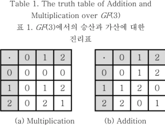
Table 1 shows the truth table of addition and multiplication over GF(3).
Table 1. The truth table of Addition and Multiplication over GF(3)
표 1. GF(3)에서의 승산과 가산에 대한 진리표
․ 0 1 2
0 0 0 0
1 0 1 2
2 0 2 1
․ 0 1 2
0 0 1 2
1 1 2 0
2 2 0 1
(a) Multiplication (b) Addition
2.2 Multiplication algorithm for AOTPover GF(3) A polynomial of the form (1) over GF(3) is called an all one or two polynomial (AOTP) of degree m if
A Study on the Parallel Multiplier over GF(3m) Using AOTP 3
2 1 or
ai= for i= 0,1,2,....,m.
m
am
a a
a
A= 0 + 1α + 2α2+"+ α (1)
Suppose that α is a root of an irreducible AOTP of degree m. Two elements, multiplier A and multiplicand B in the Galois field GF(3m) can be represented as (2).
m
am
a a
a
A = 0 + 1α + 2α2+ " + α
m
bm
b b
b
B = 0 + 1α + 2α2 + " + α (2)
where, the coordinates a ,i bi ∈ GF(3) for m
i≤
≤
0 and {1,α,α2,...,αm} are the extended basis of GF(3m).
Then the inner product of A and B is defined as (3)
) (
) (
) (
) (
0 0
2 2 1 0
2 2 1 0
∑
∑= • =
=
+ + + +
•
+ + +
+
=
•
m i
i i m
i i i
m m
m m
b a
b b
b b
a a
a a B A
α α
α α
α
α α
α
"
"
(3)
(3) is represented as (4) by replacing the product term with R.
∑
∑
∑= = = +
+
=
=
+ + + +
=
m m i
i i m
i i i m
i i i
m m
r r
r
r r
r r R
2 1 0
2 0
2 2 2
2 1 0
α α
α
α α
α "
(4) The second term of (4) can be represented as (5) b y the multiplication property of finite field.
m m i i m m
i i
m i
i i m m m m
i i i
m i
i i m m
i i i
r r
r
r r
r
r r
R
α α
α α
α
α α
+ +
=
+ +
=
+
=
+ +
−
=
−
= ++
−
=
−
= ++
=
∑
∑
∑
∑
∑
)
( 1
1 0
1
0 1
1 0
1
0 1
0
(5)
In (5), let ri+rm+i+1=Ri,rm=Rm, (5) is represented as (6).
∑− ∑
= + = =
= 1
0 0
m i
m i
i i m
m i
i R R
R
R α α α
(6)
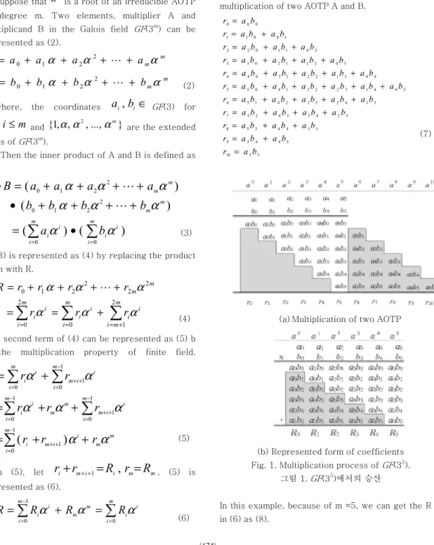
For example, the inner product of two polynomials of GF(35) is represented as (7) by the definition and Fig. 1 shows the process of the multiplication of two AOTP A and B.
5 5 10
5 4 4 5 9
5 3 4 4 3 5 8
5 2 4 3 3 4 2 5 7
5 1 4 2 3 3 2 4 1 5 6
5 0 4 1 3 2 2 3 1 4 0 5 5
4 0 3 1 2 2 1 3 0 4 4
3 0 2 1 1 2 0 3 3
2 0 1 1 0 2 2
1 0 0 1 1
0 0 0
b a r
b a b a r
b a b a b a r
b a b a b a b a r
b a b a b a b a b a r
b a b a b a b a b a b a r
b a b a b a b a b a r
b a b a b a b a r
b a b a b a r
b a b a r
b a r
= +
=
+ +
=
+ + +
=
+ + + +
=
+ + + + +
=
+ + + +
=
+ + +
=
+ +
= +
=
=
(7)
(a) Multiplication of two AOTP
(b) Represented form of coefficients Fig. 1. Multiplication process of GF(35).
그림 1. GF(35)에서의 승산
In this example, because of m =5, we can get the R in (6) as (8).
5 5 4 4 3 3
2 2 1 1 0 0
α α α
α α α
α
R R R
R R R
R
R i i
+ +
+
+ +
=
=∑
(8)
Riare given by (5) and (6) as (9).
5 5 10
4 4
9 3 3 8
2 2
7 1 1 6
0 0
, , ,
r R r
r R
r r R r
r R
r r R r
r R
= +
=
+
= +
=
+
= +
=
(9) with (7), (9) is represented as (10).
5 0 4 1 3 2
2 3 1 4 0 5 5
5 5 4 0 3 1
2 2 1 3 0 4 4
5 4 4 5 3 0
2 1 1 2 0 3 3
5 3 4 4 3 5
2 0 1 1 0 2 2
5 2 4 3 3 4
2 5 1 0 0 1 1
5 1 4 2 3 3
2 4 1 5 0 0 0
b a b a b a
b a b a b a R
b a b a b a
b a b a b a R
b a b a b a
b a b a b a R
b a b a b a
b a b a b a R
b a b a b a
b a b a b a R
b a b a b a
b a b a b a R
+ + +
+ +
=
+ + +
+ +
=
+ + +
+ +
=
+ + +
+ +
=
+ + +
+ +
=
+ + +
+ +
=
(10)
III. AOTP based Multiplier
This section presents the multiplication and addition gate which is the two main elements of the basic cell in the multiplier over GF(3m). The Down-Literal Circuit(DLC) [9] is mainly used to design the ternary gates. The multi-threshold property of DLC is applied with pass transistor logic.
3.1 The structure of multiplication gate
A multiplication gate follows the modular 3 multiplication operation over GF(3m), and the result value is obtained as Table 2 according to
multiplication truth table shown in Table 1. Fig. 2 shows the block diagram of the proposed multiplication gate.
Vx and Vy are the input voltage signals of the gate and the bias voltages are passed according to the condition of input signals. If input signals are 0 and 0, the pass transistor P33, P34, P35 and P36are ON because each output signal of DLC is high. Vout is the output voltage signal of the gate which represents the ternary output value as 0 with 0 [V], 1 with 1.5 [V] and 2 with 3 [V], respectively.
To represent the symbol of ternarymultiplication gate, we use the shape of AND gate in the binary logic because the output signals of the gate are similar to modular 3 multiplication results. To show the difference of the two gates, we added the character TMUL in the symbol. Fig. 3 shows the symbol of the multiplication gate.
D0 D1 D2 D3
VDD GND VDD GND
Vx Vy
1.5V 1.5V
Vout
P1 1.5V
VDD GND VDD 1.5V GND GND GND GND
P2 P3 P4
P5 P6 P7 P8
P9 P10 P11 P12
P13 P14 P15 P16
P17 P18 P19 P20
P21 P22 P23 P24
P25 P26 P27 P28
P29 P30 P31 P32
P33 P34 P35 P36
I0 I1 I2 I3
Fig. 2. The block diagram of ternary multiplication gate.
그림 2. 3치 승산 게이트의 블록도
A Study on the Parallel Multiplier over GF(3m) Using AOTP 5
Table 2. Output signal value of ternary multiplication gate
표 2. 3치 승산 게이트의 출력 신호표
Vout Vx Vy D0 D1 D2 D3
1 2 2 L L L L
2 1 2 L H L L
0 0 2 H H L L
2 2 1 L L L H
1 1 1 L H L H
0 0 1 H H L H
0 2 0 L L H H
0 1 0 L H H H
0 0 0 H H H H
Fig. 3. The symbol of ternary addition gate.
그림 3. 3치 승산 게이트의 심벌
3.2 The structure of multiplication gate
In the same manner as the multiplication gate, addition gate mainly consists of DLC and pass transistors. Addition gate follows the modular 3 addition operation over GF(3m), and the result value is obtained as Table 3 according to addition truth table shown in Table 1. Fig. 4 shows the block diagram of the proposed addition gate. And Fig. 5 shows the symbol of addition gate. We use the shape of Ex-OR gate in the binary logic because the output signals of the gate are similar to modular 3 addition results. To show the difference of the two gates, we added the character TADD in the symbol.
D0 D1 D2 D3
VDD GND VDD GND
Vx Vy
1.5V 1.5V
Vout
1.5V VDD
GND VDD 1.5V
GND GND
VDD 1.5V
P1 P2 P3 P4
P5 P6 P7 P8
P9 P10 P11 P12
P13 P14 P15 P16
P17 P18 P19 P20
P21 P22 P23 P24
P25 P26 P27 P28
P29 P30 P31 P32
P33 P34 P35 P36
I0 I1 I2 I3
Fig. 4. The block diagram of ternary addition gate.
그림 4. 3치 가산 게이트의 블록도
3.3 Multiplier basic cell
In order to implement the AOTP multiplier over
Fig. 5. The symbol of ternary addition gate.
그림 5. 3치 가산 게이트의 심벌
Table 3. Output signal value of ternary addition gate 표 3. 3치 가산 게이트의 출력 신호표
Vout Vx Vy D0 D1 D2 D3
1 2 2 L L L L
0 1 2 L H L L
2 0 2 H H L L
0 2 1 L L L H
2 1 1 L H L H
1 0 1 H H L H
2 2 0 L L H H
1 1 0 L H H H
0 0 0 H H H H
GF(3m), we applied a multiplication algorithm over finite field GF(3m), and constructed the multiplier basic cell using addition and multiplication gate described in a previous section.
Fig. 6 shows the block diagram of basic cell in the multiplier over GF(3m). The cell input signals ai
and birepresent the coefficients of the multiplier polynomial A and the multiplicand polynomial B, respectively. X is the other input signal which stems from the previous cell, and Y is the output signal of the cell.
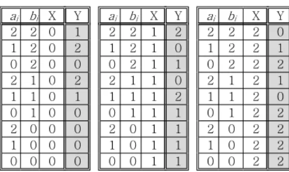
Table 4 shows all 27 cases of the basic cell in the ternary multiplier. Signal flows are like this, first, the cell input ternary signals ( ai and bi) are
multiplied by ternary multiplication gate, and then the previous cell's output X and the output signal of multiplication gate are added by ternary addition gate. The output signal Y is not only the output of this stage but also the input signal of the next stage. In the multiplier, the cell's operation is processed iteratively.
ai
bi bi
ai
TMUL X
Y TADD
Fig. 6. Basic cell of multiplier over GF(3m).
그림 6. GF(3m)상에서의 승산기 기본 셀
Table 4. Output signal value of basic cell in the ternary multiplier
표 4. 3치 승산기내 기본 셀의 촐력 신호표 ai bi X Y
2 2 0 1
1 2 0 2
0 2 0 0
2 1 0 2
1 1 0 1
0 1 0 0
2 0 0 0
1 0 0 0
0 0 0 0
ai bi X Y
2 2 1 2
1 2 1 0
0 2 1 1
2 1 1 0
1 1 1 2
0 1 1 1
2 0 1 1
1 0 1 1
0 0 1 1
ai bi X Y
2 2 2 0
1 2 2 1
0 2 2 2
2 1 2 1
1 1 2 0
0 1 2 2
2 0 2 2
1 0 2 2
0 0 2 2
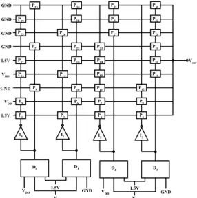
3.4 The structure of ternary multiplier over GF(3m)
This section presents the parallel-in parallel-out systolic architecture for computing ternary multiplication over GF(3m) in which the elements are represented with a root of an irreducible AOTP of degree m. For simplicity, the GF(35) is used as example to illustrate the operation.
Fig. 7 shows the structure of ternary multiplier over GF(35). ai, biand Rirepresent the coefficients of the multiplier polynomial A and the multiplicand polynomial B and multiplication result polynomial, respectively. The input 0 of the first stage represent that no input signals exist before the first stage.
IV.SimulationresultsandComparision
The proposed ternary multiplier circuit has been simulated by HSPICE with model parameter for Hynix 0.35umCMOS process. Logical levels of the ternary input voltage(0,1,2)areassigned as 0, 1.5, 3 [V] and the reference voltages of the DLC block are 0 [V], 1/2Vdd = 1.5 [V], and Vdd = 3V, respectively.
A Study on the Parallel Multiplier over GF(3m) Using AOTP 7
b0
b1
b3
b5
a3
a0 0 0 0 0 0 0
b2
b4
a1 a2 a3
a4
a5
a5
a4
a2
a1
R0 R1 R2 R3 R4 R5
TCELL TCELL TCELL TCELL TCELL TCELL
TCELL TCELL TCELL TCELL TCELL TCELL
TCELL TCELL TCELL TCELL TCELL TCELL
TCELL TCELL TCELL TCELL TCELL TCELL
TCELL TCELL TCELL TCELL TCELL TCELL
TCELL TCELL TCELL TCELL TCELL TCELL
Fig. 7. The structure of AOTP multiplier over GF(35).
그림 7. GF(35)상에서의 AOTP 승산기 구조
4. 1. Simulation results of gates
The input signals of the gate, Vx and Vy, are shown in Fig. 8(a) and (b), respectively. The cycle of the input signal is assigned as 300 [ns] and rising time as 10 [ns].
(a) Input signal Vx in the gate
(b) Input signal Vy in the gate Fig. 8. Input signals of the ternary gates
그림 8. 3치 게이트의 입력신호
Fig. 9 (a) and (b) show the output of the multiplication gate and addition gate. Simulation results represent the Vout of the table 3 and table 4, respectively. The output signals show 9 different stages in the table.
(a) The output signal of the multiplication gate
(b) The output signal of the addition gate Fig. 9. Output results of the ternary gates
그림 9. 3치 게이트의 출력신호
4. 2. Simulation results of the basic cell
The input signals of the basic cell, Vx and Vy, are shown in Fig. 10 (a), (b), and (c), respectively. The cycle of the input signal is assigned as 300 [ns] and rising time as 10 [ns]. Fig. 10(d) shows the output of the basic cell. Simulation result represents the Y of the Fig. 6 and table 4. The output signals show 27 different stages in the table 4.
(a) Input signal Vx in the basic cell
(b) Input signal Vy in the basic cell
(c) Input signal X in the basic cell
(d) Output signal Y in the basic cell Fig. 10. Simulation results of the basic cell in
ternary multiplier.
그림 10. 3치 승산기의 기본셀 출력 결과
4. 3. Multiplication over GF(3m)
Assume that the coefficients of the AOTP A and B are a0=2, a1=2, a2=1, a3=2, a4=1, a5=2 and b0=1, b1=1, b2=2, b3=1, b4=2, b5=1. According to (3)-(8), the product of the multiplication A and B over GF(3m) can be obtained by (11).
5 4 3 2
5 5 4 4 3 3
2 2 1 1 0 0
2 2
2α α α α α
α α
α
α α
α
+ + + +
=
+ +
+
+ +
=
•
R R
R
R R
R B A
(11) In this case, the coefficient outputs of the product result are static values, so we abbreviate the simulation results in this paper.
4. 4. Comparison
This section presents the compared data processing ability between the previous studies and this study.
We assumed that gates are same in all multipliers and focused on the number of gate in the multipliers. On condition that all multipliers calculates the same amount of information data, a multiplier over GF(3m) has the 1.5 times better data processing ability than a multiplier GF(2m).
Though the proposed multiplier shows the similar number of gate with Lee's, the amount of processed data will be larger than that with the same propagation delay time.
Table 5 shows the structure comparison between this work and the previous works.
Table 5. Structure comparison table of multipliers 표 5. 승산기 구조 비교표
V. Conclusions
In this paper, we have defined a ternary multiplication algorithm with AOTP over GF(3m) and designed the parallel-in parallel-out systolic multiplier circuit with using DLC and pass transistor logic.
Proposed multiplier has been constructed with lower number of gates and performs 1.5 times more information processing with comparing it with multipliers over GF(2m).
Simulations of the proposed ternary multiplier circuit were done by using HSPICE with model parameter for the Hynix 0.35m CMOS process. With the 3 [MHz] sampling rate, multiplier shows 4 [uW]
power dissipation.
The layout of the proposed circuit is one of our further studies and extension of field over GF(pm) is expected.
Multipliers Items
Yeh[2]
GF(2m) Lee[7]
GF(2m)
This paper GF(3m) Gates per cell
AND, 2 input EX-or, 2 input Ex-OR, 2 input 1 bit latch
2 2 0 7
1 1 0 3
1 1 0 0 Total Gates
AND, 2 input EX-or, 2 input Ex-OR, 2 input 1 bit latch
2m2 2m2 0 7m2
(m+1)2 (m+1)2
0 (m+1)2
(m+1)2 (m+1)2
0 0 Gates with m = 5
AND, 2 input EX-or, 2 input Ex-OR, 2 input 1 bit latch
50 50 0 175
36 36 0 144
36 36 0 0
A Study on the Parallel Multiplier over GF(3m) Using AOTP 9
VI. References
[1] S. L. Hurst, "Multiple-valued logic-its future,"
IEEE Trans. Computers, vol 30, pp. 1161-1179, Dec. 1984.
[2] C. S. Yeh, I. S. Reed, and T.K. Truong, "Systolic Multipliers for Finite Fields GF(2m )," IEEE Trans. Computers, vol. 33, no. 4, pp.
357-360, Apr. 1984.
[3] P. A. Scott, S. E. Tarvares, and L. E. Peppard,
"A fast multiplier for GF(2m )," IEEE J.Select.
Areas Commun., vol. SAC-4, Jan. 1986.
[4] E.D. Mastrovito, "VLSI Architectures for Multiplication Over Finite Field GF(2m ) ," Applied Algebraic Algorithms, and Error-Correcting Code, Proc. Sixth
Int'l Conf., AAECC-6, T.Mora,ed., pp.297-309,Rome, July 1988.
[5] E.D. Mastrovito, "VLSI Architectures for Computation in Galois Fields," PhD thesis, Linkoping Univ., Dept. of Electrical Eng., Linkoping, Sweden, 1991.
[6] B. Sunar, and C.K. Koc, "Mastrovito Multiplier for All Trinomials," IEEE Trans. Comput., vol.
c-48, No. 5, pp.522-527, May 1999.
[7] C. Y. Lee, E. Lu, and J. Y. Lee, "Bit-Parallel Systolic Multiplier for GF(2m) Fields Defined by All-One and Equally Spaced Polynomials," IEEE Trans. Comput., vol. 50, No. 5, pp.385-393, May 2001.
[8] N. Muranaka, S. Arai, S. Imanishi, and D. M.
Miller,"A Ternary Systolic Product-Sum Circuit for GF(3m) using Neuron MOSFETs,"
Proc. 29th ISMVLpp. 180-185, Freiburg Germany, May 1999.
[9] J. shen and K. Tanno and O. Ishizuka,"Down Literal circuit with Neuron-MOS Transistors and Its Applications," Proc. 29th ISMVL pp. 180-185, Freiburg Germany, May 1999.
저 자 소 개
한 성 일 (韓 聖 一)
제 7권 2호 논문 03-01-13 참조 2004년 3월 - 현재 : 인덕대학 정보통신전공 전임강사
주관심분야 : 전자통신, 회로설계, VLSI 설계, 통신 알고리즘
황 종 학 (黃 鍾 學)
1988년 : 인하대학교 전자공학과 학사.
1990년 : 인하대학원 전자공학과 석사.
2001년 : 인하대학원 전자공학과 공학박사.
1990 - 1992년 : (주)필코 부설 연구소 연구원.
1992년 - 1995년 : 나우정밀 중앙연구소 전임연구원.
1996년 - 현재 : 체육과학연구원 책임연구원.
주관심분야 : 이동통신, 스포츠용 기구, VLSI 설계, 모 터 자동제어