한국표면공학회지 J. Korean Inst. Surf. Eng.
Vol. 51, No. 4, 2018.
https://doi.org/10.5695/JKISE.2018.51.4.197
<연구논문>
ISSN 1225-8024(Print) ISSN 2288-8403(Online)
동적 나노압침법을 이용한 Ni-P 도막의 특성 연구
정무영a, 백열a, 강보경a, 최용a,*, 권혁주b
a단국대학교 신소재공학과, b한스코 연구개발부
(Received 7 June, 2018 ; revised 1 August, 2018 ; accepted 9 August, 2018)
Characterization of Electro-deposited Ni-P Layer by Using Dynamic Nano-Indentation Method
Moo Young Junga, Youl Baika, Bo Kyeong Kanga, Yong Choia,*, and Hyuk Joo Kwonb
aDepartment of Materials Science and Engineering, Dankook University, Dandae-ro 119, Dongnam-gu, Cheonan, Chungnam 31116, Republic of Korea
bR&D Center, HANSCO, 35 Munpyeongseo-ro 17 gil, Daedeok-gu, Daejeon, 34303
Abstract
Dynamic nano-indentation method was applied to characterize thin electroformed Ni-P layers. The Ni-P layers were produced in a sulphamic acid bath at 50oC in 0.02 A/cm2 for 10-60 minutes. The chemical analyses by XRD and EDX showed that the Ni-P layers were very fine grains with mainly Ni3P with Ni. The surface roughness determined by atomic force microscopy increased with thickness, which was relative to the surface morphology. The nano-hardness and the stiffness of the thin Ni-P layers with thickness of 1.9, 6.2 and 7.5µm were 5.52, 6.52 and 6.77 [GPa] and 56.7, 76.2 and 108.0 [µN/nm], respectively. The elastic modulus of the Ni-P layer increased with thickness such as 37.29, 54.50 and 78.76 [GPa], respectively. The surface rough- ness of the electroplated Ni-P layers with diverse thickness was 8.66, 18.56 and 35.22 [nm], respectively.
The enhanced nano-mechanical properties were related to mainly residual stress of the Ni-P layers.
Keywords : Ni-P deposit, Dynamic nano-indentation method
1. Introduction
Nanocrystalline nickel-phosphorus (Ni-P) alloys deposits are used in electronic and automobile components for their good corrosion and wear property[1-2]. For the preparation of the Ni-P deposits, the electrolyte and the electro-less deposition methods are generally used [3]. Since the electro-less deposition takes more deposition time and more precise controlled process, the electrolytic deposition
method to make Ni-P nanocrystalline layer is preferred for more efficiency in a filed [4].
One of problems to prepare the Ni-P deposit by the electrolytic deposition is a high residual stress in the deposit so that it tends to make surface cracks and becomes a problem of electroforming for the production of the very thin layers because of its brittleness [5-6]. Although the high residual stress of the electro-deposits can be controlled by electroplating conditions like current density and additives [7-10], little information is available about the fabrication of the thin Ni-P layers by electroforming. Recently, dynamic indentation method has been attractive attention to characterize the thin layers because it can evaluate not only surface
*Corresponding Author: Yong Choi
Department of Materials Science and Engineering, Dankook University
Tel: +82-41-529-6187 ; Fax: +82-41-559-7866 E-mail: [email protected]
hardness but also friction force and surface stiffness.
Accordingly, various nano-mechanical properties of the electroformed Ni-P thin layers like surface stiffness and friction force can give more precise strengthening mechanism to control residual stress of the thin layers. Hence, the objectives of this study are to make thin Ni-P layers by electroforming with adding surfactants and characterize the Ni-P layer by dynamic nano-indentation method to give the strength mechanism of the electroformed layers.
2. Experimental method
The 304 stainless steel pale was used for the electroforming substrate. The 304 stainless steel substrates was electrolytic polished in 0.2N sulfuric acid (H
2SO
4) to eliminate the resident debris and get a lowest surface roughness before the electroforming of the Ni-P deposit [10]. The Ni-P electroforming was carried out at 50
oC and 0.02 A/cm
2in a modified sulphamic acid solution. Table 2-1 is the chemical components of the bath which contains nickel sulfamate and phosphorous acid at the pH values of 2.0.
The phase identification and chemical analysis were performed by XRD (Iedx-150T, Isp co., Korea) and EDX (Noran, Thermo, USA), respectively. Phase identification was carried out at the condition of the diffraction angle from 30
oto 100
o, step rate of 0.02
o/ sec, and Cu·K α line at room temperature. Rietveld refinement of the XRD data was carried out by the analysis software, Fullprof 2014 (ILL, France).
Surface morphology are observed by SEM (CX- 200TA, Coxem, Korea) and AFM (Pafm nx II, Em4sys C. Ltd, Korea), respectively. Nano- mechanical property of the electroformed Ni-P layers was determined by scanning probe micoscopy (TI- 750, Hysitron, USA).
3. Results and discussions
3.1. Chemical analysis
Table 3-1-1 is the chemical composition of the electroformed Ni-P layers with different plating time.
The ratio of the Ni and P content is about 87 and 13 [wt.%], which is almost equal to the Ni-P layers in error range.
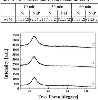
Fig. 3-1-1 is XRD spectra of the electroformed Ni- P deposit with plating time. As shown in Fig. 3-1-1, the peak broadening is present from the diffraction angles of 30
oto 60
odegrees. It means that the Ni-P deposits contain very fine crystalline. The highest
diffraction peak at 44.3
odegree stands for the Ni phase, whereas, the diffraction peaks at 50.72
oand 66.86
ocorrespond to the Ni
3P phase. Accordingly, the electroformed Ni-P deposit has Ni and Ni
3P phases. In order to quantitatively analysis of the compositions, Rietveld refinement of the XRD spectra was conducted for Ni and Ni
3P phases because the solubility of P in Ni is little in Ni-P binary phase diagram. Table 3-1-2 is the composition of the electroformed Ni-P deposit with plating time.
As shown in Table 3-1-2, the ratio of the Ni to Ni
3P phases is almost equal to various thickness of the Ni- P layers, which composition is mainly Ni
3P with small amount of Ni phases. The amount of Ni and Ni
3P are 17 and 83 [%], respectively.
Table 2-1. The conditions and the major components of the bath for electrolyte deposition of Ni-P layer.
Parameter Amount
Nickel Sulfamate Solution [mL] 300 Phosphorous acid [g/L] 27
pH 2
Temperature [oC] 50
Table 3-1-1. The compositions of the electroformed Ni-P deposits with plating time
10 min 30 min 60 min
Ni [wt.%] 84.16(2) 85.67(2) 84.36(2) P [wt.%] 13.79(2) 12.34(2) 13.28(2)
Table 3-1-2. Rietveld analysis of electroformed Ni-P
10 min 30 min 60 min
Ni Ni3P Ni Ni3P Ni Ni3P wt % 17.76(2) 82.24(2) 17.77(2) 82.23(2)17.77(2)82.23(2)
Fig 3-1-1. The XRD spectra of the electroplated Ni-P deposits with plating time: (a) 10 (b) 30 (c) 60 [min]
3.2. Microstructure
Fig. 3-2-1 is the surface morphologies of the electroformed Ni-P deposits with different plating time. Fig. 3-2-1 (a), (b), (c) are the surfaces with 10 min, 30 min, 60 min plating time, respectively. As shown in Fig. 3-2-1-(a), it is difficult to observe nodules on the surface of the plate formed for
10 min, whereas, lots of nodules are present on the surface of the thick layers. It means that the thicker the deposit is, the more nodules are, as shown in Fig.
3-2-1-(b) and (c).
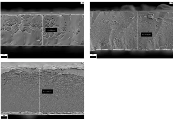
Fig. 3-2-2 is the cross section image of the electroformed Ni-P deposits with varied plating time by SEM. As shown in Fig. 3-2-2, the thickness of
Fig 3-2-1. The surface morphologies of the electroformed Ni-P deposits with varied plating time: (a) 10 (b) 30 (c) 60 [min]Fig 3-2-2. The cross section image of the electroformed Ni-P deposits with plating time: (a) 10 (b) 30 (c) 60 [min]
the electroformed Ni-P deposits was about 1.9, 6.2 and 7.5 mm, respectively. Although the average growth rate of the Ni-P deposit is almost 3 ×10
-3μm/
sec, it tends to be decreased with thickness. As shown in Fig. 3-2-2-(a) to the Fig. 3-2-2-(b), a rapid increase of thickness was observed at the initial stage of growth such as the plating time from 10 to 30 minutes, which is related to electrical field on the deposit [11]. In this study, the relation between thickness and plating time was determined as following equation(1), which x and y are thickness [ μm] and plating time [sec] of Ni-P films, respectively.
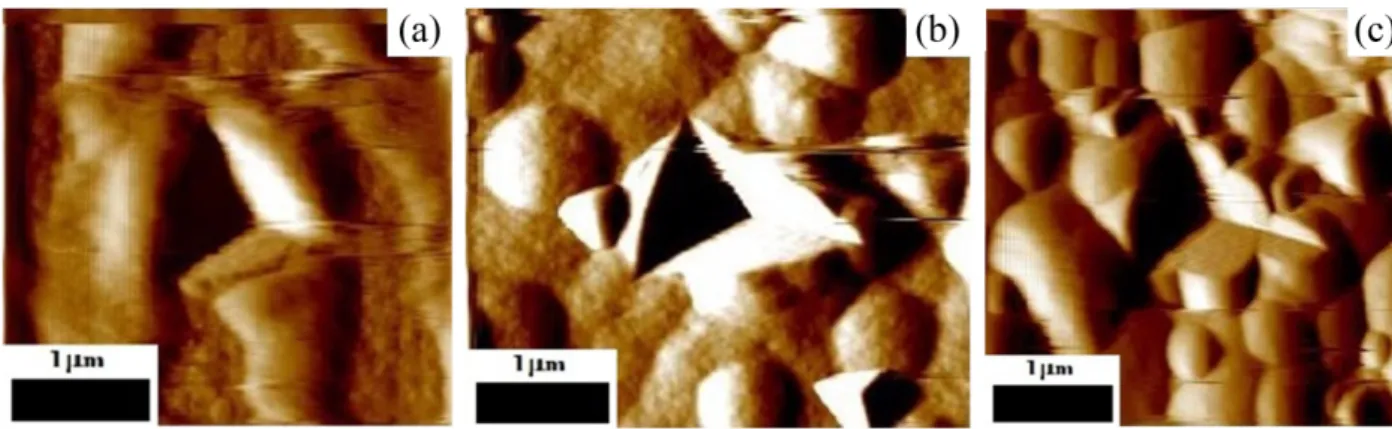
(1) Fig. 3-2-3 shows the surface morphologies of the different thickness of the Ni-P layers with indented mark. As shown in Fig. 3-2-3, the indented mark has a symmetry, which means the indent tip is vertically dented on the surface of the Ni-P layers. As shown in Fig. 3-2-3 and Table 3-3-1, the surface roughness of the electroplated Ni-P with thickness is 8.66, 18.56 and 35.22 [nm]. The surface roughness of the electroplated Ni-P layer increases with thickness because of increasing nodules with it.
3.3 Nano-mechanical property
In order to obtain the nano-mechanical properties of electroplated Ni-P films with different thickness, the dyanamic nano-indentation test was performed.
Fig. 3-3-1 is the load-displacement curves of electroplated Ni-P films with thickness. Table 3-3-1 is the results of the hardness, stiffness and elastic modulus of the different thickness of the Ni-P layers.
The hardness of electroplated Ni-P films with increasing thickness is 5.52, 6.52 and 6.77 [GPa]. In
accordance with thickness, the elastic modulus of electroplated Ni-P is 37.29, 54.50 and 78.76 [GPa].
In compliance with thickness, the stiffnesses of the electroformed Ni-P layers was calculated by the initial slopes of the unloading section in the load- displacement curves in Fig 3-3-1, are 56.7, 76.2 and 108.0 [μN/nm], respectively. Table 3-3-1 is summarized of the nano-mechanical properties. As shown in Table 3-3-1, the mechanical hardness, the stiffness and the elastic modulus of the electroformed NI-P layers increased with thickness. The hardening on the Ni-P deposits may be induced with the solid solution hardening, and residual stress [12]. Since the y = 5.21ln x ( ) 2.08 +
Fig 3-2-3. Surface morphologies of the electroplated Ni-P films with thickness: (a) 1.9 (b) 6.2 (c) 7.5 [µm]
Fig 3-3-1. the load-depth curves of the Ni-P deposited electrically by nano-indentor with plating time: (a) 10 (b) 30 (c) 60 [min]
Table 3-3-1. The mechanical properties of the electroplated Ni-P films with plating time.
Hardness [GPa]
Stiffness
[µN/nm] Er [GPa]
Rq [nm]
10 min 5.52(2) 56.7(2) 37.29(2) 8.66(2) 30 min 6.52(2) 76.2(2) 54.50(2) 18.56(2) 60 min 6.77(2) 108.0(1) 78.76(2) 35.22(2)
P content in Ni matrix is almost equal to 13 wt.%, the solid-solution hardening effect is equal to the different thickness of the Ni-P layer. In case of residual stress, it is dependent upon the elastic stiffness and modulus. Since both the elastic stiffness and the modulus increase with the thickness of the Ni-P deposit, it supports that their hardness increase is related to the residual stress of the electroformed Ni-P layers.
4. Conclusions
(1) The electroformed Ni-P layers prepared in a modified sulphamic acid bath are very fine crystalline. Their composition are about 87 wt.% Ni and 13 wt.% P, which is almost equal to the different thickness of the layers. The final phase of the electroformed Ni-P layers are mainly Ni
3P and small minorly Ni.
(2) The thickness of the electroformed Ni-P layers with 10, 30 and 60 minute are 1.9, 6.2 and 7.5 [ μm].
The average deposit rate is almost 3 ×10
-3μm/sec.
Their surface roughness of the electroplated Ni-P with thickness is 8.66, 18.56 and 35.22 [nm], respectively.
(3) The nano-hardness, the elastic modulus and the stiffness of the electroformed Ni-P layers with 1.9, 6.2 and 7.5 [ μm] thick are 5.52, 6.52, 6.77 [GPa] and 37.29, 54.50, 78.76 [GPa] and 56.7, 76.2, 108.0 [ μN/
nm], respectively.
Acknowledgement
This study was financially supported by the Industrial Cooperation Technical Development Project of the Ministry of Small and Medium Enterprises and Startups (MSS) (Grant # C0530921).
One of authors thanks for the Nuclear Power Core Technology Program of the Korea Institute of Energy Technology Evaluation and Planning (KETEP), which is being funded by the Ministry of Trade, Industry & Energy, Republic of Korea (No.
20141710201690).
References
[1] H.B. Lee, D.S. Wuu, C.Y. Lee, C.S. Lin, Wear and Immersion Corrosion of Ni-P Electrodeposit
in NaCl Solution, Tribology International, 43 (2010) 235-244.
[2] Myung-Hee Choi, Young Bae Park, Byong ho Rhee, Eungsun Byon, Kyu Hwan Lee, Effect of Heat Treatment on Interface Behavior in Ni-P/Cr Double Layer, Journal of the Korean Institute of Surface Engineering, 48 (2015) 260-264.
[3] Amir Ahmadi Ashtiani, Soheila Faraji, Sepideh Amjad Iranagh, Amir Hossein Faraji, The Study of Electroless Ni-P with Different Complexing Agents on Ck45 Steel Substrate, Arabian Journal of Chemistry, 10 (2017) 1541-1545.
[4] P. Peeters, G.v.d. Hoorn, T. Daenen, A. Kurowski, G. Staikov, Properties of Electroless and Electroplated Ni-P and its Application in Microgalvanics, Electrochimica Acta, 47 (2001) 161-169.
[5] Kazimierz Czapczyk, Piotr Siwak, Piotr Jablonski, Luksz Furmanski, Pawel Grobelny, Stanislaw Legutko, Influence of the Thickness of Ni-P Coating Applied on 7075 Aluminum Alloy on its Hardness, Advances in Science and Technology, 10 (2016) 53-58.
[6] Cheng-Hsun Hsu, Sheng-Chien Chiu, Yih-Hsun Shih, Effects of Thickness of Electroless Ni-P Deposit on Corrosion Fatigue Damage of 7075- T6 under Salt Spray Atmosphere, 45 (2004) 3201- 3208.
[7] Moo Hong Seo, Dong Jin Kim, Joung Soo Kim, The Study on Residual Stresses of Ni Alloy Electrodeposits for Steam Generator Tube Repair, Proceedings of the Korean Nuclear Society Autumn Meeting, 35 (2003).
[8] G. Mcmahon, U. Erb, Structural Transitions in Electroplated Ni-P alloys, Journal of Materials Science Letters, 8 (1989) 865-868.
[9] Raj Narayan, M.N. Mungole, Electrodeposition of Ni-P Alloy Coatings, Surface Technology, 24 (1985) 233-239.
[10] A.P. Ordine, S.L. Diaz, I.C.P. Margarit, O.E. Barcia, O.R. Mattos, Electrochemical Study on Ni-P Electrodeposition, Electrochimica Acta, 51 (2006) 1480-1486.
[11] R. Rofagha, U.Erb, D.Ostrander, G. Palumbo, K.T.
Aust, The Effects of Grain Size and Phosphorus on the Corrosion of Nanocrystalline Ni-P Alloys, Nanostructured Materials, 2 (1993) 1-10.
[12] N. Du M. Pritzker, Investigation of electroless plating of Ni–W–P alloy films, Journal of Applied Electrochemistry, 33 (2003) 1001-1009.