I. INTRODUCTION
In recent year, the research on multiple-valued logic(MVL) has attracted attention of logic designers because it can increase the information density of circuits, and thus leading to the reduction of the
number of connections and pins, and the saving of on-chip area of IC[1,2]. However, it also leads to the complexity in designing and analyzing circuits along with the increase of the number of signal levels. Among the various types of MVL, the ternary logic is one of the most popular logic because of the simpler circuit implementations and lower interconnections cost estimations[1].
Several static and dynamic ternary logic circuits have been proposed. The circuit realization of MVL gates using I2L, charge-coupled devices, voltage-mode CMOS, current-mode CMOS
* 인하대학교 전자공학과
(Dept. of Electronics Eng., Inha University)
** 카톨릭대학교 정보통신전자공학부
接受日:2004年 2月 24日, 修正完了日:2004年 6月 28日
A Design of a Ternary Storage Elements Using CMOS Ternary Logic Gates
CMOS 3치 논리 게이트를 이용한 3치 저장 소자 설계
Byoung-Hee Yoon*, Gi-Young Byun**, Heung-Soo Kim* 尹 炳 熙*, 卞 基 寧**, 金 興 壽*
Abstract
We present the design of ternary flip-flop which is based on ternary logic so as to process ternary data.
These flip-flops arecomposed with ternary voltage mode NMAX, NMIN, INVERTER gates. These logic gate circuits are designed using CMOS and obtained the characteristics of a lower voltage, lower power consumption as compared to other gates. These circuits have been simulated with the electrical parameters of a standard 0.35um CMOS technology and 3.3Volts supply voltage. The architecture of proposed ternary flip-flop is highly modular and well suited for VLSI implementation, only using ternary gates.
key word : ternary logic gates, ternary flip-flop, power consumption
요 약
본 논문에서는 3치 논리 게이트를 바탕으로 하는 3치 데이터 처리를 위한 3치 flip-flop을 설계하였다. 제안한 flip-flop들은 3치 전압 모드 NMAX, NMIN, INVERTER 게이트를 사용하여 설계하였다. 또한 CMOS 기술을 사 용하였고 다른 게이트들 보다 낮은 공급 전압과 낮은 전력소모 특성을 포함하고 있다. 제안한 회로는 0.35um 표 준 CMOS 공정에서 설계되었고 3.3v의 공급 전압원을 사용하였다. 제안된 3치 flip-flop 구조는 3치 논리 게이트를 사용하여 VLSI 구현에 적합하고 높은 모듈성의 장점을 갖고 있다.
technologies was reported in the literature[3]-[9].
These circuits are generally multiple-powered circuits and they require complex processing to fabricate both depletion and enhancement CMOS transistors [10] or multi-threshold transistor.
Complex multiphase clocking scheme may also be required in the case of dynamic circuits .
In this paper, a new voltage-mode CMOS ternary logic circuit and a ternary flip-flop design method using these are presented. It thus minimizes spikes and offers low power supply noise advantages over other implementations. The circuit may be useful in mixed-mode integrated circuits whose performance accuracy is limited by the effects of the digital switching noise generated by the digital circuits. In addition, the proposed circuits require a single power supply.
The circuit descriptions of the basic gates are presented and their static and dynamic performance characteristics have been investigated using HSPICE simulations.
There are three logic values (0,1,2) for signals in these circuits. So, when analyzing ternary circuits, we must consider the response to six transitions of input signals between three voltage levels as well as the response of circuits to three values of input signals.
II. Design of ternary flip-flop
2.1 Basic operation of MVL function
The operations of conjunction and disjunction are used for implementation of MVL function[11]. We define the conjunction and disjunction for two variables, x, y {0,1,2,, P-1}
MIN operation x∧y = MIN(x,y) MAX operation x∨y = MAX(x,y) Inverter operation x'= (N-1) - x
Where, conjunction MIN(x,y) is the minimum value of variables, x,y and disjunction MAX(x,y) is the maximum value of variables, x, y. x' is the complement of x, N means the radix of this circuit.
2.2 Ternary basic flip-flop (TFF)
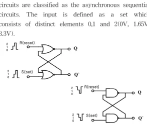
TFF circuit can be constructed from two ternary NMIN(Negation-MIN) gates or two ternary NMAX (Negation-MAX) gates. These constructions are shown in the logic diagramsof Fig. 1 and characteristic table for the basic TFF is in Table1.
It defines the logical property of the flip-flop. The circuit forms a basic flip-flop upon which other gate constitutes a feedback path. For this reason, the circuits are classified as the asynchronous sequential circuits. The input is defined as a set which consists of distinct elements 0,1 and 2(0V, 1.65V, 3.3V).
그림 1. 기본 TFF 논리 다이어그램 Fig.1. Logic Diagram of basic TFF circuit.
표 1. 특성표 Table 1. Characteristic Table
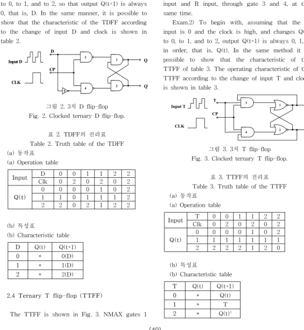
2.3 Ternary D flip-flop (TDFF)
The TDFF shown in Fig. 2 is the modification of the ternary basic flip-flop. NMIN gates 1 and 2 form a basic flip-flop and gates 3, 4 and 5 connected with that, form the TDFF of Fig. 2, we must remember that the output of a ternary NMIN gate is always 2 if any input is 0, and the output is 0 when both of two inputs are 2. When each of
R 0 0 0 1 1 1 2 2 2
S 0 1 2 0 1 2 0 1 2
Q(t+1) Q(t) 2, if Q(t)=2
1, otherwise 2 0, if Q(t)=0
1, otherwise 1 1 0 0 0 Q
Q`
0 1 2
0 1 2
R(reset)
S(set)
Q
Q`
0 1 2
0 1 2
R(reset)
S(set)
inputs is 1 and 1, 1 and 2, 2 and 1, the output is 1.
We define that when the clock is a high-level signal, the logical value of the clock is 2, and if the clock is a low-level signal, that of the clock is 0.
The value of input D goes directly to the S input, and its complement, through inverter, is applied to the R input.
Exam. 1) As a starting point, assume that the D input is 0 and the clock is high, and changes Q(t) to 0, to 1, and to 2, so that output Q(t+1) is always 0, that is, D. In the same manner, it is possible to show that the characteristic of the TDFF according to the change of input D and clock is shown in table 2.
1
2 3
5 4
Q
Q`
D
CP Input D
CLK
그림 2. 3치 D flip-flop Fig. 2. Clocked ternary D flip-flop.
표 2. TDFF의 진리표 Table 2. Truth table of the TDFF (a) 동작표
(a) Operation table
Input D 0 0 1 1 2 2
Clk 0 2 0 2 0 2
Q(t)
0 0 0 0 1 0 2
1 1 0 1 1 1 2
2 2 0 2 1 2 2
(b) 특성표
(b) Characteristic table
D Q(t) Q(t+1)
0 * 0(D)
1 * 1(D)
2 * 2(D)
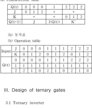
2.4 Ternary T flip-flop (TTFF)
The TTFF is shown in Fig. 3. NMAX gates 1
and 2 form a basic flip-flop and gates 3 and 4 connected with that, form the TTFF.In order to analyze the operating characteristic of the TTFF of Fig. 3, we must know that the output of a ternary NMAX gate is always 0 if any input is 2, and the output is 0 when both of two inputs are 0. In case of the values of two inputs are 01, 11, and 10, that is the output is 1.
The value of input T goes directly to the S input and R input, through gate 3 and 4, at the same time.
Exam.2) To begin with, assuming that the T input is 0 and the clock is high, and changes Q(t) to 0, to 1, and to 2, output Q(t+1) is always 0, 1, 2 in order, that is, Q(t). In the same method it is possible to show that the characteristic of the TTFF of table 3. The operating characteristic of the TTFF according to the change of input T and clock is shown in table 3.
1
2 3
4
Q
Q`
T CP Input T
CLK
그림 3. 3치 T flip-flop Fig. 3. Clocked ternary T flip-flop.
표 3. TTFF의 진리표 Table 3. Truth table of the TTFF (a) 동작표
(a) Operation table
(b) 특성표
(b) Characteristic table
T Q(t) Q(t+1)
0 * Q(t)
1 * T
2 * Q(t)`
Input T 0 0 1 1 2 2
Clk 0 2 0 2 0 2
Q(t)
0 0 0 0 1 0 2
1 1 1 1 1 1 1
2 2 2 2 1 2 0
2.5 Ternary of JK flip-flop (TJKFF)
The TJKFF is shown in Fig. 4, it is the extension of the ternary basic flip-flop. NMAX gates 1 and 2 form a basic flip-flop and gates 3 and 4 connected with that, form the TJKFF. To analyze the operating characteristic of the TJKFF of Fig. 4, the output of a ternary MIN gate is always 0 if any input is 0, and the output is 2 when both of two inputs are 2. When each of inputs is 11, 12 and 21, the output is 1, that is to say, that of a ternary MIN gate is obtained by the operation of conjunction, MIN(x,y)
The input J and K behave like inputs S and R to set and clear the flip-flop(note that in a JK flip-flop, the letter J is for set and the letter K is for clear).
For example, in the first place, assuming that the present output Q(t) is 0 and the clock is high, and changes each of the input J and K to 0, to 1, and to 2, the next output Q(t+1) depends entirely on the input J, having no connection with the input K.
In the same method, if the Q(t) is 1, it depends on the Q(t), unconcerned with the input J and the input K. When Q(t) is 2, the output Q(t+1) counts on the complement of the input K, except the input J.
In this method, the operating characteristic of the TJKFF according to the change of the input J, the input K and the clock is shown in table 4.
1
2 3
4
Q
Q`
K CP Input J
and K
CLK
J
그림 4. 3치 JK flip-flop Fig. 4. Clocked ternary JK flip-flop.
표 4. TJKFF의 진리표 Table 4 Truth table of the TJKFF (a) 특성표
(a) Characteristic table
Q(t) 0 0 0 1 2 2 2
J 0 1 2 * *
K * * 0 1 2
Q(t+1) J 1(Q(t)) K`
(b) 동작표 (b) Operation table
Input J 0 0 0 1 1 1 2 2 2
K 0 1 2 0 1 2 0 1 2
Q(t)
0 0 0 0 1 1 1 2 2 2
1 1 1 1 1 1 1 1 1 1
2 2 1 0 2 1 0 2 1 0
III. Design of ternary gates
3.1 Ternary inverter
The circuit of the ternary inverter gate using voltage mode CMOS logic circuits is shown in Fig.
5. It is designed by NMOS and PMOS, like as binary inverter. The output inverting each input is obtained by using the complement operation.
The power supply voltage is 3.3V, each of the input signals(or output signals) is 0V, 1.65V and 3.3V. And the logical values 0, 1 and 2 correspond to 0V, 1.65V and 3.3V. The operating characteristic of the ternary inverter circuit is shown in table 5 and its HSPICE simulation results are shown in Fig.
6.
VIN VOUT
VDD
그림 5. 3치 인버터 회로 Fig. 5. The ternary inverter circuit.
표 5. 3치 인버터의 진리표
Table 5. Truth table of the ternary inverter gate
IN OUT
0 2
1 1
2 0
그림 6. 3치 인버터의 모의실험 Fig. 6. Simulation result of ternary inverter.
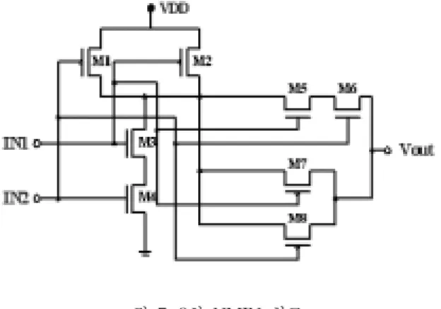
3.2 Ternary NMIN gate
The circuit of the ternary NMIN gate using voltage mode CMOS logic circuits is shown in Fig.
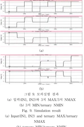
7. Note that the M1~M4 form an ordinary NAND and M5~M8 form switching circuit. When IN1 and IN2 have the logical value of 1 or 2, higher than threshold voltage, M5 and M6 operate normally. And M5, M6 generate 1.65V by the regulation of transistor size properly. Therefore, in case that IN1 and IN2 have the logical values of 11, 12 and 21, the output voltage is 2(3.3V). The operating characteristic of the ternary NMIN circuit is shown in table 6 and its simulation results are shown in Fig. 9.
표 6. 3치 NMIN 게이트의 진리표 Table 6. Truth table of ternary NMIN gate
그림 7. 3치 NMIN 회로 Fig. 7. The ternary NMIN circuit
3.3 Ternary NMAX gate
The circuit of the ternary NMAX gate is shown in Fig. 9. Where, the M1~M4 form an ordinary NOR and M5~M8 form switching circuit. When the inputs IN1 and IN2 have the value of 0 or 1, lower than threshold voltage, PMOS transistor M5 and M6 operate normally. PMOS transistor M1 and M2 operate in the logical value of 1 like doing in that of 0 with increasing the size of transistor.
Therefore, when each of input IN1 and IN2 is 00, 01, 10 and 11, the circuit formed with M1~M4 generate output, 2(3.3V). On the other hand, when IN1 and IN2 are only the logical values 0 and 0, the M5 and M6 operate and generate output voltage 3.3V. M7 and M8 operate if the value of any input is a logical value 1(1.65V), M7 and M8 on.
The truth table of the ternary NMAX circuit is shown in table 7 and its simulation results are shown in Fig. 9.
표 7. 3치 NMAX 게이트의 진리표 Table 7. Truth table of ternary NMAX gate 0
0 2 2 2
2 2
1 1
1 1
1 0
2
2
IN2 IN1
0
0 2 1 0
1 0
1 1
1 0
0 0
2
2 IN2 IN1
M1 M2
M3 M4
M5 M6
M7
M8
Vout IN1
IN2
VDD
그림 8. 3치 NMAX 회로 Fig. 8. The ternary NMAX circuit.
(a)
(b)
그림 9. 모의실험 결과
(a) 입력(IN1, IN2)와 3치 MAX/3치 NMAX (b) 3치 MIN/ternary NMIN
Fig. 9. Simulation result
(a) Input(IN1, IN2) and ternary MAX/ternary NMAX
(b) ternary MIN/ternary NMIN
IV. Comparison and conclusion
In this paper, the switched voltage CMOS ternary
logic gates and the ternary flip-flop using that logic gates have been described. The performance characteristics of the logic gates are investigated by using HSPICE simulations. The obtained results indicate that the proposed circuits exhibit good noise margin of about 15% of the power supply voltage and propagation delay times of less than 1ns in most case. The propagation delay can be improved by increasing the supply voltage and the aspect ratios of the transistors used, at the expense of increased power consumption. A detailed comparison, among the proposed circuit, the circuit reported by Nagata[3], Shousha[4], is shown in Table 8.
표 8. 제안된 논문과 [3], [4]의 비교표 Table 8. Comparison among the proposed,
[3] and [4]
This circuits have advantages in the point of view : ← Less interconnections, ↑Operate at the lower supply voltage, →Less power consumption(about 1uW).
Results for deep sub-micron technologies(0.35um) show the effects of the method for future multiple-valued processes. Also, the proposed ternary flip-flops were presented by a new and an efficient circuit design methodology. Namely, these flip-flops can be more easily implemented in the gate level than in the MOSFET level. The performance of the proposed ternary logic gates is shown in Table 9.
Comparison Shousha[4] Nagata[3] Proposed Operation
method
MIN, MAX Complement
MIN, MAX Complement
MIN, MAX Complement CMOS tech. CM 1.0um VM 2.0um VM 0.35um
No. CS 1 0 0
No. VS 1(5V) 2(4V, 2V) 1(3.3V)
No. Tr.
TINV : 7 TNMAX: 10 TNMIN : 10
TINV 3 + SOI 1 TNMAX 6 + SOI 1 TNMIN 10 + SOI 1
TINV :2 TNMAX : 8
TNMIN:8
표 9. 제안된 3치 기본 논리게이트의 성능 Table 9. The performances of the proposed ternary
basic logic gates
The implementation of the flip-flop circuits and the remove of the glitch in the gate circuits will be the next theme of this paper.
References
[1] S.L. Hurst, "Multiple-valued logic Its status and its future,"IEEE Trans. on Computer, vol. C-22, pp. 1160-1179, 1984.
[2] M. Davio, "Synthesis of discrete functions using I2L technology,"IEEE Trans. on Computer, vol. C-30, pp. 653-661, sept. 1981.
[3] Yasunori Nagata, "Design of an Asynchronous Digital System with B-ternary Logic," Proc. 27th ISMVL, pp.
256-271, May 1997.
[4] A.H. Shousha, "Switched current CMOS ternary logic circuits,"Int. J. Electronics, vol . 79, No. 5, pp. 617-625, 1995.
[5] A. Jain, "CMOS multiple valued logic design part I : Circuit implementation," IEEE Trans. Circuit system, vol. 40, pp. 503-514, Aug. 1993.
[6] A. Jain, "CMOS multiple valued logic design part II : Function realization,"IEEE Trans.
Circuit system, vol. 40, pp. 515-522, Aug.
1993.
[7] Y.J. Chang, "Synthesis of multi-variable
MVL functions using hybrid mode CMOS logic," Proc. 24th ISMVL, pp. 35-41, May.
1994.
[8] K.W. Current, "Multiple valued logic : Current-mode CMOS circuits," Proc. 23th ISMVL, pp. 176-181, May. 1993.
[9] C.Y. Wu, "Design and application pipe lined dynamic CMOS ternary logic and sample ternary differential logic," IEEE J.
Solid-state circuit, vol. 28, pp. 895-906, Aug.
1993.
[10] P.C. Ballar, "Low power dissipation MOS ternary logic family," IEEE J. of Solid-state circuit, vol.19, pp. 739-749, 1984.
[11] X.W. Wu, "CMOS ternary logic circuits,"Proc. of the Institution of Electrical Engineers, PtG. 137, pp. 21-27, 1990.
저 자 소 개
윤 병 희 (尹 炳 熙, Byoung-Hee Yoon) 제 7권 제 1호 논문 03-01-05 참조 인하대학교 전자공학과 박사수료
변 기 영 (卞 基 寧, Gi-Young Byun) 제 6권 제 1호 논문 02-01-04 참조
카톨릭대학교 정보통신전자공학부 강의전담교수
김 흥 수(金 興 壽, Heung-Soo Kim) 제7권 1호 논문 03-01-05 참조 인하대학교 전자공학과 교수 MIN/NMIN MAX/NMAX Inverter
Technology CMOS n-well 0.35m
CMOS n-well 0.35m
CMOS n-well 0.35m
Power supply 3.3V 3.3V 3.3V
Time delay
(worst case) 1.2ns/1.4ns 1.0ns/1.2ns 1.0ns Power
dissipation 1uW 1.2uW 0.6uW