Design Optimization of Ball Grid Array Packaging by the Taguchi Method
Yeong K. Kim†, Jae-chang Kim and Joo Ho Choi
School of Aerospace and Mechanical Engineering, Korea Aerospace University, 100 Hanggongdae-gil, Hwajeon-dong, Deogyang-gu Goyang-city, Gyeonggi-do 412-791, Korea
(Received December 6, 2010: Accepted December 20, 2010)
Abstract: In this paper, a design optimization of ball grid array packaging geometry is studied based on the Taguchi method, which allowed robust design by considering the variance of the input parameters during the optimization process.
Molding compound and substrate were modeled as viscoelastic, and finite element analyses were performed to calculate the strain energy densities of the eutectic solder balls. Six quality factors of the dimensions of the packaging geometry were chosen as control factors. After performing noise experiments to determine the dominant factors, main experiments were conducted to find the optimum packaging geometry. Then the strain energy densities between the original and optimized geometries were compared. It was found that the effects of the packaging geometry on the solder ball reliability were significant, and more than 40% of the strain energy density was reduced by the geometry optimization.
Keywords: Reliability, Optimization, Viscoelasticity, Taguchi method
1. Introduction
The progress toward the compactness of modern microelectronics devices faces numerous challenges in various engineering areas. Among these, thermal and mechanical reliability has been a primary issue over the last decades. As well known, the mechanical stresses develop due to the heterogeneous nature of the component materials in the packaging structure, which results in behaviors mismatch under environmental changes. For the evaluation of the packaging reliability, experimental methods such as accelerated testing are widely adopted.1, 2) Although the methods are relatively simple and robust, the time and cost for the prototype manufacturing are substantial. In addition, it is not easy to obtain the stress development mechanism, which is essential to improve the packaging structure reliability. To overcome this drawback, numerical simulation has been widely employed to analyze, understand and predict the mechanical failure. However, the prediction of the simulation results are occasionally different from the experimental data, mainly due to inappropriate modeling of mechanical material properties such as elastic assumptions for viscoelastic materials.
Comprehensive analyses and discussions on this subject were reported by Kim et al..3) They showed that, in addition to the better results, the viscoelastic calculations provided in-depth insights in understanding the stress development mechanism. They also demonstrated that the elastic calculations
could lead to inappropriate prediction in ‘what-if’ study.
Recently, efforts to enhance the mechanical reliability of solder joints have been extended to optimal geometry design through statistical methods such as design of experiments (DOE) and the Taguchi method.4-10) The studies calculated the strain energy densities of the solder balls as quality characteristics, and changed the geometry dimensions of the component material structures. However, all the previous results were based on the elastic approaches where the viscoelastic material properties of the molding compound and the substrate were modeled as elastic.
The objective of this study was to explore a design optimization of the ball grid array packaging structure based on the viscoelastic calculations. The material properties of the molding compound and the substrate were measured and modeled as viscoelastic. Using the data, simulations based on viscoelastic finite element method were performed under accelerated thermal cycles to yield the strain energy densities of the solder balls. The Taguchi method11) was employed for the geometry optimization, and six different dimensions such as the thickness of the materials and solder pitches were considered as quality factors. Strain energy density of the solder ball was employed as objective function. After the optimization, the energy densities of the original packaging and optimized packaging were compared for the evaluation.
†Corresponding author E-mail: [email protected]
2. Modeling
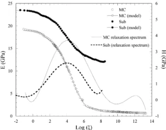
For the simulation, a typical PBGA packaging structure was modeled as a three dimensional strip. Fig. 1 shows the packaging structure with relevant dimensions. The packaging structure involved molding compound to encapsulate the silicon chip, and thin FR-4 substrate of an epoxy/glass fabric composite material was considered. The viscoelastic material properties were readily measured in the previous work,3) and the results are presented in Fig. 2 and Fig. 3. As seen, the molding compound exhibited strong viscoelastic
behavior, and the substrate also showed viscoelastic characteristics, although it was not strong as the molding compound. The glass transition temperatures of the molding compound and the substrate were 105oC and 175oC, respectively. Mastercurves of the materials were also measured by a series of stress relaxation tests based on viscoelastic theory. The data are represented in Fig. 3, where the solid lines represent the moldeings by exponential function series (a.k.a. Prony series). And the corresponding shift functions are shown in Fig. 4. The parameters of the mastercurve modelings and the shift functions are listed in Ref. 3. Other mechanical properties such as coefficients of thermal expansion and Poisson’s ratios of the molding compound and the substrate, and the elastic properties of the silicon and copper are listed in Table 1. Due to the lack of data, the printed circuit board (PCB) was assumed as elastic for this preliminary study, and also listed in Table 1. To examine the relaxation behavior, relaxation time spectra were calculated using the Alfrey approximation12) as
(1)
Equation (1) indicates that the relaxation spectrum can be obtained from the slope of the mastercurve without complex calculations. The results are also plotted in Fig. 3. The peak relation times of the molding compound and the substrate are 104.5 minutes and 103.9 minutes, respectively, indicating that the two materials have similar relaxation behaviors.
In the simulation, ANSYS (v. 12.1) was used for the strain energy density calculations using solid 185 elements for the entire modeling. The solder balls were assumed as Sn40Pb solder alloy, and Anand’s model parameters were
H t( ) d E t( ( )) d(log( )ξ ) ---
ξ t=
= Fig. 1. The geometry and element distribution of the ball grid array
package (3D geometric modeling). The solder balls are numbered for their identities. (Unit: mm)
Fig. 2. Dynamic mechanical analysis results of the molding compound and the substrate.
Fig. 3. Mastercurves and relaxation spectrum of the molding compound and substrate.
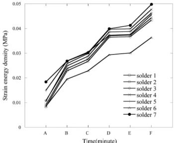
employed for the constitutive equation.13) To evaluate the fatigue process, the individual strain energy densities accumulated in the solder balls illustrated in Fig. 1 were calculated. The thermal cycles used for the simulations are shown in Fig. 5. The temperature cooled down from 170oC to room temperature to simulate the molding compound cure, and one more cycle was added after the cooldown.
The cooling and heating rates were about –5oC/min and 5oC/min, respectively. The strain energy densities were calculated during the thermal cycle, and recorded at six different times to trace the energy density accumulations.
Fig. 6 shows the strain energy density accumulation profiles for the solder balls. As seen, the energy density increased as the thermal cycle proceeded, and the highest value was found in the solder ball no. 4.
2.1. Optimization
The Taguchi optimization process employed in this study was similar to the work by Lai and Wang.6) Six quality control factors and their levels were chosen, as listed in Table 2. All the factors had three levels: Level 2 is the original dimensions, and Level 1 and Level 3 were reduced and increased thicknesses. The Taguchi method was employed to reduce the number of experiments, and L27 (36) orthogonal array was obtained for the main experiments.
The smaller-the-better signal to noise (S/N) was defined as
(2)
where yi is the ith measurement data and r is the number of measurements. In this study, the objective function was the accumulated strain energy density of the solder ball at the point F in Fig. 5. In the actual calculations, the numerical results do not contain experimental errors.
Therefore, artificial data errors were generated by intentional deviations in the noise experiments by imposing
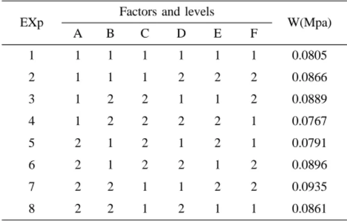
±4% noise on the control factors. In Table 3, two-level noise factors were implemented in an L8 (26) orthogonal array in which level 1 and level 2 stood for the corresponding noise factor with -4% and +4% noises, respectively.
Table 4 and Fig. 7 show the responses calculated from the results presented in Table 3. In Table 4, level i of factor j is
S N⁄ –10log Σi=1
r yi
2
---r
=
y≡W Table 1. Elastic mechanical properties of the component materials
of the PBGA packaging structure. MC and Sub represent the molding compound and the substrate, respectively.
E (GPa) Poisson’s Ratio CTE (ppm/oC) Tg
MC 0.26 α1: 14.5
α2:56.6 105oC
Sub 0.27 11e-6 175oC
Silicon 160 0.23 2.6e-6
PCB 22 0.28 12.7e-6
Cu 130 0.34 17.8e-6
Fig. 4. Shift functions of the molding compound and substrate.
Fig. 5. Temperature cycle profile for strain density calculations.
defined as the average of W of factor j at level i. Table 4 and Fig.7 show that solder joint pitch was the most effective noise factor. Therefore, we defined three sets of artificial
experimental errors to be implemented on the solder ball pitch in the main experiments. For this, same errors of ±4%
were applied for each level of the solder joint pitch, which formed the L27 (36) orthogonal array for the main experiments.
The calculation results based on these errors are listed in Table 2. Control factors and levels (unit: mm).
Factor Type Level 1 Level 2 Level 3
A Molding compound thickness 0.25 0.4 0.55
B PCB thickness 1 1.2 1.4
C Substrate thickness 0.1 0.2 0.3
D Solder ball height 0.35 0.4 0.45
E UBM diameter 0.35 0.45 0.55
F Solder joint pitch 0.85 1 1.15
Table 3. Noise experiments.
EXp Factors and levels
W(Mpa)
A B C D E F
1 1 1 1 1 1 1 0.0805
2 1 1 1 2 2 2 0.0866
3 1 2 2 1 1 2 0.0889
4 1 2 2 2 2 1 0.0767
5 2 1 2 1 2 1 0.0791
6 2 1 2 2 1 2 0.0896
7 2 2 1 1 2 2 0.0935
8 2 2 1 2 1 1 0.0861
Table 4. Results of the noise experiments
Level A B C D E F
1 0.08318 0.08395 0.08668 0.0855 0.08628 0.0806 2 0.08708 0.0863 0.08358 0.08475 0.08398 0.08965 Effect 0.0039 0.00235 0.0031 0.00075 0.0023 0.00905
Rank 2 4 3 6 5 1
Fig. 6. Strain energy density accumulations of the original packaging structure under the thermal cycles.
Table 5. Results of main experiments.
S/N Factors and levels
A B C D E F N1 N2 N3 S/N
1 1 1 1 1 1 1 0.0982 0.103 0.108 19.7311 2 1 1 1 1 2 2 0.0915 0.095 0.0985 20.4416 3 1 1 1 1 3 3 0.117 0.12 0.124 18.3898 4 1 2 2 2 1 1 0.0702 0.0737 0.0773 22.64 5 1 2 2 2 2 2 0.0684 0.0709 0.0735 22.9793 6 1 2 2 2 3 3 0.084 0.0864 0.0887 21.2709 7 1 3 3 3 1 1 0.0641 0.0676 0.0712 23.3888 8 1 3 3 3 2 2 0.0563 0.0586 0.0609 24.6376 9 1 3 3 3 3 3 0.0616 0.0632 0.0649 23.9791 10 2 1 2 3 1 2 0.101 0.108 0.115 19.3194 11 2 1 2 3 2 3 0.0891 0.0938 0.0986 20.5454 12 2 1 2 3 3 1 0.056 0.0938 0.0593 22.8817 13 2 2 3 1 1 2 0.107 0.114 0.121 18.851 14 2 2 3 1 2 3 0.102 0.107 0.111 19.4343 15 2 2 3 1 3 1 0.0922 0.0927 0.0933 20.6552 16 2 3 1 2 1 2 0.156 0.166 0.177 15.5689 17 2 3 1 2 2 3 0.134 0.142 0.15 16.9451 18 2 3 1 2 3 1 0.0893 0.0913 0.0933 20.7892 19 3 1 3 2 1 3 0.162 0.174 0.187 15.1575 20 3 1 3 2 2 1 0.068 0.0712 0.0746 22.9361 21 3 1 3 2 3 2 0.0834 0.0864 0.0894 21.2662 22 3 2 1 3 1 3 0.232 0.25 0.269 12.0138 23 3 2 1 3 2 1 0.0982 0.104 0.11 19.6445 24 3 2 1 3 3 2 0.094 0.0989 0.104 20.0828 25 3 3 2 1 1 3 0.191 0.206 0.222 13.6923 26 3 3 2 1 2 1 0.0933 0.0965 0.0998 20.3032 27 3 3 2 1 3 2 0.125 0.129 0.134 17.7623
Table 5 as N1, N2 and N3. N1 is the accumulated strain energy densities calculated by decreasing the joint pitch by 4%, and N3 by increasing joint pitch by 4 %. N2 is for the energy densities that are based on no error. The corresponding S/N values are also listed in Table 5, and plotted in Fig. 8.
Through ANOVA, the dominant factors for the optimal design were found to be A (molding compound thickness), C (substrate thickness), E (UBM diameter) and F (solder joint pitch).
Using the results, the optimum packaging structure was constructed and the maximum strain energy density accumulation was calculated again. The calculation results
are shown in Table 6, and compared with the value based on the original packaging structure. It was found that the maximum strain energy density accumulated at the thermal point F (see Fig. 5) based on the optimized dimensions was 0.0497 MPa, which is 41.5% less than the value before the optimization. The S/N ratio was also increased about 26.5%.
Fig. 9 represents the strain energy density accumulations of the individual solder balls using the optimized structure.
Unlike the original results in Fig. 6, the absolute values of the strain energy densities and their differences among the individual solder balls are noticeably smaller, and the maximum value was found in the no. 7 solder ball which was at the outmost location from the geometric center line (x=0).
3. Conclusions
In this study, the Taguchi method was successfully applied to obtain the optimized geometry for the BGA packaging structure. In this level of the structural modeling, the solder ball pitch was found to be the most effective noise factor. By applying the artificial noise to the factors, the main experiments were performed to achieve the minimum strain energy density accumulation. It was found that the maximum strain energy density based on the optimized geometry was about 40% less than that of the original packaging configuration. It was also found that the solder location of the maximum strain energy density was changed from the no. 4 solder ball to the no. 7 solder ball. Actual attempts to change the packaging dimensions such as solder ball pitches, the thicknesses of the molding compound and the substrate may Fig. 7. Responses of noise experiments diagram.
Fig. 8. Responses of main experiments diagram.
Table 6. Comparison of the strain energy densities of the original and optimized packaging structures.
Design Factors and levels
W(Mpa) S/N
A B C D E F
Original 2 2 2 2 2 2 0.0849 21.12
Optimal 1 2 3 3 2 1 0.0497 26.72
41.5% 26.5%
Fig. 9. Strain energy density accumulations of the optimized packaging structure under the thermal cycles.
need careful consideration in the industrial process application. However, this study clearly demonstrates that the effects of the packaging geometry variations on the solder ball reliability are remarkable. The analyses of the differences between the elastic and viscoelastic approaches to account for the viscoelastic behaviors of the materials as control factors are in progress.
References
1. H. Son, I. Kim, S. Lee, K. Jung, B. Park and K. Baik, “Reli- ability Studies on Cu/SnAg Double-Bump Flip Chip Assem- blies for Fine Pitch Applications”, J. Microelectron. Packag.
Soc., 15(2), 37 (2008).
2. S. Han, I. Cho and Y. Shin, “Reliability of Sn-8Zn-3Bi Solder Paste Applied to Lead and Lead-free Plating on Lead-frame under Thermal Shock Test”, J. Microelectron. Packag. Soc., 14(2), 35 (2007).
3. Y. K. Kim, I. S. Park and J. Choi, “Strip type panel warpage analyses for PBGA chip packaging”, Microelectronics Reli- ability, 50, 398 (2010).
4. C. Mao and R. Chen, “Packaging parameter analysis and opti- mization design on solder joint reliability for twin die stacked packages by variance in strain energy density (SED) of each solder joint”, Microelectronics Reliability, 48, 119 (2008).
5. T. Tee and Z. Zhong, “Board level solder joint reliability anal- ysis and optimization of pyramidal stacked die BGA pack- ages”, Microelectronics Reliability, 44, 1957 (2004).
6. Y. Lai and T. H. Wang, “Optimal design towards enhance- ment of board-level thermomechanical reliability of wafer-
level chip-scale packages”, Microelectronics Reliability, 47, 104 (2007).
7. Y. Lai, T. H. Wang and C. Wang, “Optimization of Thermo- mechanical Reliability of Board-level Package-on-Package Stacking Assembly”, IEEE TRANSACTIONS ON COMPO- NENTS AND PACKAGING TECHNOLOGIES, 29, 864 (2006).
8. T. Wang and Y. Lai, “Optimization of Thermomechanical Reliability of Board-Level Flip-Chip Packages Implemented With Organic or Silicon Substrates”, IEEE TRANSACTIONS ON ELECTRONICS PACKAGING MANUFACTURING, 31(2), 174 (2008).
9. T. Wang, Y. Lai, C. Lee, and Y. Lin, “Coupled Power and Thermal Cycling Reliability of Board-Level Package-on- Package Stacking Assembly”, IEEE TRANSACTIONS ON ELECTRONICS PACKAGING MANUFACTURING, 32(1), 14 (2009).
10. T. Wang, C. Wang, Y. Lai, K. Chang and C. Lee, “Optimi- zation of board-level thermomechanical reliability of high performance flip-chip package assembly”, Microelectronic Engineering., 85(4), 659 (2008).
11. G. Taguchi, “Quality engineering (Taguchi methods) for the development of electronic circuit technology”, IEEE Trans Reliab., 44(2), 225 (1995).
12. I. Ward and D. Hardley, An Introduction to the Mechanical Properties of Solid Polymers, John Wiley & Sons Ltd., United Kingdom (1993).
13. G. Wang, Z. Cheng, K. Becker and J. Wilde, “Applying Anand Model to Represent the Viscoplastic Deformation Behavior of Solder Alloys,” Journal of Electronics Packaging, 123, 247 (2001).