Simple LCD CCFL-backlight Resonant Inverter
Gang-Youl Jeong
1*1Department of Electronic Information Engineering, Soonchunhyang University
간단한 LCD CCFL백라이트 공진형 인버터
정강률
1*1순천향대학교 전자정보공학과
Abstract This paper presents a simple LCD CCFL-backlight resonant inverter. First, in introduction various conventional inverter topologies for the CCFL are reviewed, briefly, and then, in each main subject the proposed inverter is explained, in detail. The proposed inverter utilizes a new class-E resonant circuit with a single-switch and is controlled by a single-chip microcontroller, which is very simple. Moreover, the proposed inverter can ensure resonant zero voltage switching (ZVS) under most operating conditions and performs simply the digital dimming control. It is shown through experimental results that the proposed inverter has good performance for the LCD CCFL-backlight.
요 약 본 논문에서는 간단한 LCD CCFL백라이트 공진형 인버터를 제안한다. 먼저 서론에서 다양한 전통적 CCFL 인버터의 토폴로지들을 간략하게 살펴보고, 그 다음 각 본론에서 제안한 인버터에 대하여 구체적으로 설명한다. 제안 한 인버터는 단일스위치를 가진 새로운 E-계열 공진회로를 이용하며 단일칩 마이크로컨트롤러에 의해 제어된다. 그
리하여 제안한 컨버터는 매우 간단하다. 더욱이 제안한 컨버터는 대부분의 동작조건에서 공진 영전압스위칭을 확보
할 수 있으며 디지털 디밍제어를 간단하게 수행한다. 제안한 인버터가 LCD CCFL백라이트 인버터로 좋은 성능을 가 지고 있음을 실험결과를 통하여 보인다.
Key Words : LCD CCFL-backlight, Resonant inverter, Single-chip microcontroller, ZVS, Digital dimming control.
*Corresponding Author : Jeong, Gang-Youl([email protected])
Received August 4, 2010 Revised January 3, 2011 Accepted January 13, 2011
1. Introduction
The proliferation of liquid crystal display (LCD) monitors and notebook computers places an ever increasing demand on display technology. The LCD with cold cathode fluorescent lamp (CCFL) best satisfies display performance, size, efficiency and cost.
The best method of driving a load with a characteristic such as the CCFL is a current source type. When the CCFL is in compliance (open-circuit) state, the voltage can rise to the avalanche onset level. Then, as soon as ionization occurs, the voltage will collapse and the desired operating point will be reached immediately and unambiguously. Single frequency component sinusoidal
drive is preferred to maximize efficiency and minimize electromagnetic interference (EMI) [1].
The inverter that drives the CCFL is powered by 8~20 Vdc from batteries or an adaptor. The CCFL requires 1~2 kV to fire, and its inverter efficiency and size are extremely critical. The CCFL typically operates with sinusoidal voltage of 700~800 Vrms and current of 7~10 mArms. The operation frequency is normally recommended between 25~85 kHz, and a sinusoidal lamp voltage waveform is preferable. Also, the dimming control capability is another very desirable feature for such applications. These formidable requirements demand a highly efficient conversion topology and maximum circuit integration [2-5].
The most frequently used conventional CCFL-backlight inverter circuit topology is the push-pull current-source parallel-resonant inverter (CSPRI) with a buck converter added for power regulation. In CSPRI circuits used for powering CCFL, the output voltage is sine wave, and the timing is usually based on the resonance of the transformer’s magnetizing inductance and a capacitance in parallel with the primary winding [6]. The CSPRI/
buck-preregulator combination has several disadvantages such as 1) low efficiency due to two power switches in series, 2) reduced efficiency due to distorted lamp voltage and current, 3) large EMI due to hard-switching buck preregulator and unrelated switching frequencies of the preregulator and the inverter, and 4) high cost due to complex circuit topology and expensive control IC.
The current synchronous zero voltage switching (CS-ZVS) half-bridge inverter [7] is more efficient than CSPRI/buck preregulator combination, but it has also a rather complex topology, with two controlled switches, two magnetics, and three capacitors in the power train.
Other drawbacks of the circuit are that 1) the leakage inductance of the transformer is not absorbed in the load network, leading to significant lamp voltage distortion and reduced efficacy, 2) the topology is claimed to be proper and can be used only with an expensive single-source dedicated control IC, and 3) when used a dedicated control IC, the inverter requires complementary metal- oxide semiconductor field effect transistors (MOSFETs), or alternatively it would require a floating driver.
The class-E single-switch inverter is based on the conventional class-E circuit topology [8,9]. The circuit has many advantages compared with the CSPRI/buck- preregulator combination and CS-ZVS half-bridge inverter circuits. The advantages are that 1) only one switch is required, 2) the leakage inductance of the transformer is absorbed in the load network, 3) the inverter is fed with an inductance, therefore the interference current reflected back to the source is small, 4) the switch voltage waveform is smooth with a low dv/dt, so the capacitive interference is reduced, and 5) the topology is public domain.
In this paper, a simple LCD CCFL-backlight resonant inverter is proposed. First, this paper has reviewed the various inverter topologies for the CCFL in this section and then, explains the proposed inverter in the following
sections, in detail. Because the proposed inverter utilizes a new E-class inverter circuit and its control technique using a single-chip microcontroller, its circuit configuration is very simple. The proposed inverter is able to ensure ZVS operation under most operating conditions and performs simply the digital dimming control. It is also shown through experimental results that the proposed inverter has good performance for the LCD CCFL- backlight.
2. Proposed converter
The resonant inductor in the conventional class-E single-switch inverter is in series with the primary winding of the output transformer. This allows the absorption of the leakage inductance of the transformer in the resonant network, which leads to the reduction of the overall cost. Based on this, the resulting new class-E inverter variation of the proposed inverter is induced.
vin
S
Cr
T
Dr
RL
1 : n vr
iload iin
(a) The real circuit of the proposed inverter.
vin
S
Cr
ideal T Llk2
Dr
RL
1 : n Llk1
Lm
iload iin
vr
(b) The analytic model of the inverter with integrated magnetic structure.
[Fig. 1] The circuit topology used in the proposed inverter.
As shown in Fig. 1(a), the topology used in the proposed inverter is to modify the conventional class-E single-switch inverter circuit. It consists of a switch S with a built-in anti-parallel diode Dr, a resonant capacitor
Cr and a transformer T that feeds the load RL, where RL
denotes an equivalent resistor of the CCFL. To make the inverter as simple as possible, the transformer and inductor as one element is considered, which are that the combined magnetic device is viewed as two loosely coupled inductors wound on one core. This integrated magnetic structure can be represented by the analytic model shown in Fig. 1(b), which is widely used in power electronics. In this model, the transformer T in Fig. 1(a) comprises the ideal transformer ideal T, the magnetizing inductance Lm, and the primary and secondary leakage inductance Llk1 and Llk2, respectively.
The basic operation of the inverter is analyzed by considering the simplified equivalent model of Fig. 2, where the secondary leakage inductance Llk2 and load RL
are reflected to the primary, and the magnetizing inductance Lm is replaced by a current source Im. The latter is justified under the assumption that the impedance of Lm is much larger than the total reflected impedance of the secondary.
Llk2 n2 vin
RL Llk1
n2 Im
iin
niload S
CDrr vr
[Fig. 2] The simplified model of the inverter for the analysis.
Llk2 n2 vin
RL Llk1
n2 Im
vr iin
niload iin
(a) The boost mode.
Llk2 n2 vin
Cr RL
Llk1
n2 Im
vr iin
niload iCr
(b) The resonance mode.
[Fig. 3] The operational modes of the inverter.
As shown in Fig. 3, the inverter has two operational modes: the boost mode and the resonance mode, and Fig.
4 shows its theoretical operation waveform.
During the boost mode in Fig. 3(a), either the switch or the diode is conducting. In this time interval, the capacitor is shorted to ground and the reflected load current niload at the reflected branch increases exponentially. During the resonance mode in Fig. 3(b), the switch is turned off, and the inductive branch and the capacitor form a resonant network, which forces the voltage across the switch vr to follow a sinusoidal waveform. In a properly designed inverter, the sinusoidal waveform eventually returns to zero level after the anti-parallel diode catches. Then the gate drive voltage vgs
can then be applied to turn on the switch under the ZVS condition. The resonant capacitor Cr reduces the dv/dt across the switch at turn-off, which reduces switching losses and thereby allows its high frequency operation.
The theoretical analysis of the inverter is developed under the assumptions that 1) the switch, diode, capacitor, and inductor are ideal, 2) the magnetizing inductance Lm
is much larger than the leakage inductances Llk1 and Llk2, and 3) the parasitic inductances and capacitors are negligible small.
The capacitor or switch voltage vr during the resonant period Tλ can be derived from the following set of differential equations:
(1)
where Llk1 is the primary inductance, Llk2/n2 is the reflected secondary leakage inductance, Cr is the resonant capacitance, n is the turn ratio, Rr=RL/n2 is the reflected load resistor, RL is the lamp resistance, niload is the reflected load current or secondary current, and Im is the amplitude of the current source. The general solution of the set of differential equations (1) has the following form:
(2)
where Lr=Llk1+Llk2/n2, ,
, and
.The integration constants A1 and A2 are found by the boundary conditions that vr=0 at t=0 and t=Tλ. Using these conditions, the capacitor or switch voltage vr is obtained as follows:
⋅
(3)where
, θλ=ωrTλ, x=t/Tλ, and the normalized load resistance Rn=1/Q.vgs
vr
iin
iload
Ts
vin
Im
To /2
t
t
t
t = 0 t
t =Tλ t = Ts
Tλ
[Fig. 4] The theoretical operation waveform of the inverter.
At steady state, the average voltage of vr is nearly equal to Vin as follows:
(4)Using vr=0 during the Tλ<t<Ts period,
(5)where fo=ωo/2π and fs is the switching frequency.
From (5), assuming that the inverter is lossless and equating input to output power, the normalized load
current
is given by
(6)
where Iload,rms is the rms load current, and
is the characteristic impedance of the Lr-Cr resonant circuit. The theoretical results clearly point out that the inverter operates as a current source and that the output current magnitude is controlled by the switching frequency fs.3. Implementation of the proposed inverter
vin
S Cr
PWM pulse generator
Llk2
Dr RL
1 : n Llk1
Lm
OV/OC Check : vin, vr, iin, iload
- On-time calculation - Psuedo-logic 'AND'
A/D converter iload PWM OUT
iload vin
PIC16C73 Timer1 (16bit)
Iref vr iin iin
vr
Dimming Controller
[Fig. 5] The overall control block diagram of the inverter.
In the microcontroller-based control system, software flexibility facilitates the development and updating of the control technique and makes the introduction of modern control theory to obtain high performance. Moreover, the single-chip microcontroller can implement the controller with lower cost and smaller size than the general-purpose microprocessor accompanying environmental circuits.
Therefore, as shown in the Fig. 5, a low-cost 8-bit microcontroller PIC16C73 is utilized as the main controller of the proposed inverter. The measured voltage/current values at each point are inputted to the A/D converter and converted to digital values.
Main
A/D conversion : Iref, vin, vr, iin, iload
MOSFET S turn-off : PWM on-duty=0, interrupt disable Lamp dimming controller :Y
Calculation of lamp on/off duration
Min. 55kHz PWM on-duty Over current or
over voltage? Y Fault generated (fault=1)
Lamp ON?
ON OFF N
Load next Lamp OFF time
Fault:
100Hz PWM:
Load next Lamp ON time
55kHz PWM:
Timer1 interrupt Fault (fault=1) ?
N Y
Nominal 55kHz PWM on-duty
Load on-duty into the PWM pulse generator
Return
Load on-duty into the PWM pulse generator
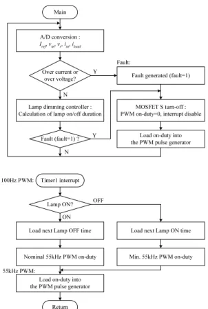
[Fig. 6] A simple flow-chart of the proposed inverter software program.
The overall inverter is divided into two parts: the controller and power circuits. The controller part includes the CPU circuit of the microcontroller PIC16C73 running the proposed control algorithms and driver circuits for driving a MOSFET. The power circuit part includes a power semiconductor switch MOSFET, a capacitor, and a transformer. The transformer turn ratio is 1:100 and its magnetizing inductance seen from the secondary winding is about 500 mH. The power semiconductor switch uses a MOSFET IRF540, whose maximum blocking voltage and drain current are 100 V and 30 A, respectively. The inverter switch is switched with high frequency, fs=55 kHz. DC input voltage is 12 Vdc and the rating lamp specification (about 6 W) is that the lamp voltage is 800 Vrms and the lamp current is 8 mArms.
100Hz
55kHz 100Hz
Lamp OFF (min. on-duty)
Lamp ON (nominnal on-duty)
Fault (logic "0", PWM OFF) 55kHz
PWM OUT
Iref
pseudo
Lamp OFF Lamp ON
[Fig. 7] The conceptual diagram of pseudo-logic ‘AND’
by the microcontroller operation.
Fig. 6 shows a simple flow-chart of the proposed inverter software program. The control software program divides into two parts: main routine and timer1 (16 bit timer) interrupt service routine. The main routine includes the A/D conversion of each voltage/current, the check of over current and over voltage, the lamp dimming controller, and the fault routine that is an infinite routine and is performed, when the controller detects over current or over voltage. The timer1 interrupt service routine is performed at each lamp turn-on/turn-off starting time, where each pulse width modulation (PWM) on-duty for the lamp turn-on/turn-off is loaded into the PWM pulse generator. The summation of the both turn-on and turn-off time durations is the lamp dimming control period Tdim=10 msec (fdim=100 Hz).
In order to control lamp brightness, two PWM pulses are modulated using the pseudo-logic ‘AND’ operation.
Fig. 7 shows the conceptual diagram of pseudo-logic
‘AND’ by the microcontroller operation. One PWM pulse frequency is 55 kHz and the other is 100 Hz. The lamp brightness is controlled by the nominal on-duty pulse area of the ‘PWM OUT’ period, which is called the digital dimming control. When the on-duty of ‘PWM OUT’ is nominal, the lamp is turned on, and when its on-duty is minimum, the lamp is turned off. This is only the conception of the pseudo-logic ‘AND’ operation.
However, when the lamp is turned off, ‘PWM OUT’
generates the minimum on-duty pulse of 55 kHz PWM for maintaining the minimum lamp current. If the minimum lamp current is maintained during the lamp turn-off period, the lamp is turned off but has the preheated effect, and thus the next initial lamp turn-on current becomes reduced. Reduction of the initial lamp turn-on current increases the CCFL’s life span [10].
Lamp ON
Timer1 interrupt
generates Next Lamp OFF time
Timer1 interrupt generates
Next Lamp ON time
t PWM
OUT
Lamp ON (nominal on-duty) Lamp OFF
Lamp OFF (min. on-duty)
t iload
[Fig. 8] The conceptual resultant waveform of ‘PWM OUT’.
The pseudo-logic ‘AND’ operation is realized by the PWM pulse generator and the timer1 interrupt. 55 kHz PWM pulse is generated through the PWM pulse generator of the microcontroller, and 100 Hz PWM is realized using the timer1 interrupt service routine. The dimming control reference signal Iref is generated by a 5 V variable resistor and is converted to digital value by the A/D converter of the microcontroller. After timer1 interrupt period calculation, the calculated digital reference value is loaded into timer1 count register. Fig.
8 shows the conceptual resultant waveform of the ‘PWM OUT’ by the pseudo-logic ‘AND’ operation, where iload is the theoretical lamp current.
4. Experimental results
In order to verify the validity of the proposed inverter, its prototype inverter has been implemented based on Section 3, and thus the following experimental results have been obtained.
(a) 25 % dimming
(b) 80 % dimming
[Fig. 9] Lamp current waveforms at each dimming state.
Fig. 9 shows the lamp current waveforms of 25 % dimming (a) and 80 % dimming (b), respectively, where the dimming means resultantly the lamp brightness. It can be seen that the initial lamp turn-on current is nearly half reduced compared with that of the conventional inverters.
[Fig. 10] Experimental waveforms of the gate drive voltage vgs and the switch voltage vr.
[Fig. 11] Experimental waveforms of the lamp voltage vlamp and the lamp current iload.
Fig. 10 shows experimental waveforms of the gate drive vgs and the switch voltage vr. These waveforms show that ZVS of the proposed inverter is achieved and the inverter well generates PWM pulses and operates stably.
Fig. 11 shows waveforms of the voltage across the lamp vlamp and the lamp current iload. These waveforms also show that the system operates well and stably.
In the experimental results of an actual 15-inch LCD monitor with the proposed inverter, the brightness was about 250 [cd/m2], and the contrast ratio was about 250:1.
These results are very similar to the CCFL BLU (Backlight Unit) performance of 15-inch class LCD monitors that are sold at a market.
5. Conclusion
In this paper, a simple LCD CCFL-backlight resonant inverter has been presented. First, this paper has reviewed the various inverter topologies for the CCFL and then has explained a modified and new E-class inverter circuit of the proposed inverter and its control technique using a single-chip micrcontroller. Because the proposed inverter utilizes a simple E-class inverter circuit with a control circuit using a single-chip microcontroller, the inverter has a very simple circuit configuration. The proposed inverter can ensure ZVS operation under most operating conditions and performs simply the digital dimming control. It has also shown through experimental results that the proposed inverter has good performance for the LCD CCFL-backlight.
참고문헌
[1] J. A. Donahue and M. M. Jovanovic, "The LCC inverter as a cold cathode fluorescent lamp driver,"
APEC 1994, Orlando, USA, pp. 427-433, 2001.
[2] G. H. Kweon, Y. C. Lim, and S. H. Yang, "An analysis of the backlight inverter by topologies,"
ISIE 2001, Pusan, Korea, pp. 896-900, 2001.
[3] S. W. Lee, D. Y. Ko, D. Y. Huh, and Y. I. Yoo,
"Simplified control technique for LCD backlight inverter system using the mixed dimming method,"
APEC 2001, Anaheim, USA., pp. 447-453, 2001.
[4] M. S. Lin, W. J. Ho, F. Y. Shih, D. Y. Chen, an Y.
P. Wu, "A cold-cathode fluorescent lamp driver circuit with synchronous primary-side dimming control," IEEE Trans. on Ind. elec., vol. 45, no. 2, pp. 249-255, 1998.
[5] R. Redl and K. Arakawa, "A low-cost control IC for sing-transistor ZVS cold-cathode fluorescent lamp inverters and DC/DC converters," APEC 1997, Atlanta, USA, pp. 1042-1049, 1997.
[6] R. L. Bright, G. F. Pittman, and G. H. Royer,
"Transistors as on-off switches in saturable-core circuits," Electrical Manufacturing, vol. 54, pp. 79-82, 1954.
[7] M. K. Nalbant, "A new and improved control technique greatly simplifies the design of ZVS resonant inverters and dc/dc converters," APEC1995, Dallas, USA, pp. 694-701, 1995.
[8] N. O. Sokal and A. D. Sokal, "Class E-a new class of high-efficiency tuned single-ended switching amplifiers," IEEE J. Solid-State Circuits, vol. SC-10, pp. 168-176, 1975.
[9] R. Redl and N. O. Sokal, "A new class-E dc/dc converter family with reduced parts count: derivation, topologies, and design considerations," HFPC 1989, San Jose, USA, pp. 395-415, 1989.
[10] G. Y. Jeong, "Simple Digital LCD Backlight Inverter using a Single-chip Microcontroller," Journal of the Korea Academia-Industrial Cooperation Society, vol. 11, no. 2, pp. 461-468, Feb. 2010.
Gang-Youl Jeong
[Regular member]• Feb. 1999 : POSTECH, Elec. &
Elec. Eng., MS
• Aug. 2002 : POSTECH, Elec. &
Elec. Eng., PhD
• Mar. 2003 ∼ current :
Soonchunhyang Univ., Dept. of Elec. Info. Eng., Associate Professor
<Research Interests>
High performance power supply, Renewable energy power supply, Motor Control