P2-100 / Z.-H. Li
• IMID 2009 DIGEST
Abstract
Cu(In,Ga)Se2 (CIGS) thin films were formed using CIGS bulk by electron-beam evaporation method with an evaporation current from 20 mA to 90 mA. The experimental results showed that the chemical compositions and the properties of CIGS films varied with the different evaporation current. The Cu-rich CIGS film was deposited successfully with a band gap of 1.20 eV when the evaporation current was 90 mA.
1. Introduction
Chalcopyrite Cu(In,Ga)Se2 (CIGS) is a potential
absorber material for high-efficiency thin-film solar cells due to its favorable band gap (1.04 eV~1.68 eV) and high-absorption coefficient (α > 104 cm-1) for
solar radiation. CIGS-based thin film solar cells with efficiencies exceeding 20% have been reported by several groups over the past few years.
A variety of processes have been proposed for the depositions of CIGS films. As a promising method for the manufacture of CIGS solar cells, two general approaches which have been used to demonstrate high device efficiencies and also in pilot scale manufacturing are discussed. One approach is the co-evaporation of the four elements such as Cu, In, Ga and Se and the other is a selenization (or two-step) for the pre-formed Cu-In-Ga film [1,2]. However, they have still several problems, such as the difficulty in controlling of the content of the evaporation sources, poor adhesion to a substrate, and the usage of harmful hydrogen selenide. In this study, we suggest the electron beam evaporation method using a Cu(In,Ga)Se2 bulk compound as another promising
candidate which offers significant advantages in terms of high directionality, stoichiometry and purity of the film.
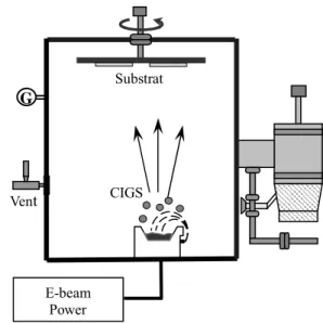
Fig. 1. Schematic of E-beam evaporation system.
2. Experimental
Cu(In,Ga)Se2 was deposited on the well-cleaned
Mo/soda-lime glass (SLG) substrates by electron beam evaporation method in a base vacuum of 1×10⁻⁵
torr. Figure 1 shows the schematic of electron-beam evaporation system. At first, Mo layer was sputtered on SLG substrate using an in-line DC magnetron sputter system with a thickness of 500 nm as a back electrode of the CIGS solar cell. The bulk alloy, Cu-In-Ga-Se compound, was evaporated from a crucible line. The thickness of the deposited film was about 1.5 µm. The energy of the incident electron beam was varied by controlling the beam current of power supply. In this experiment, the beam current to the electron gun was varied from 20 mA to 90 mA at a
Cu(In,Ga)Se
2Absorber Layer Prepared by Electron Beam
Evaporation Method for Thin Film Solar Cell
Zhao-hui Li
1, Eou Sik Cho
1, Gap Seong Noh
2, Jae Eok Lim
2,
Heui Jae Pahk
3, Kyung Bin Bae
3, and Sang Jik Kwon
1*
1
Depart. of Electronics Engineering, Kyungwon University, Seongnam, 461-701, Korea TeL: 82-31-750-5319, e-mail: [email protected]
2
Telio Solar Technoligies, Inc. , Seongnam, Kyunggi-do, Korea
3
SNU Precision Co., Ltd, Seoul, Korea
Keywords : Cu(In,Ga)Se2(CIGS), E-beam evaporation, thin film solar cell
E-beam Power G Vent Substrat CIGS
P2-100 / Z.-H. Li
IMID 2009 DIGEST • fixed voltage of 4.6 kV. In order to obtain a
well-crystallized chalcopyrite-phase Cu(In1-xGax)Se2 film,
as-deposited CIGS films were subsequently annealed at 550 °C for 1 hour in a vacuum chamber with a base pressure of 3.0×10⁻⁶ torr.
The thickness of the deposited thin films was measured using a surface profiler (Tencor Alpha-step 500). The chemical compositions of the deposited thin films were analyzed by energy dispersive X-ray analysis (EDX). The surfaces of these films were observed in a scanning electron microscope (SEM, Hitachi S-4700) and an atomic force microscope (AFM, Park Systems XE-150). The phases and crystal structure were analyzed by an X-ray diffractormeter (XRD, Rigaku D/MAX-2200) operated at 40 kV and 30 mA using Cu-kα radiation.
3. Results and discussion
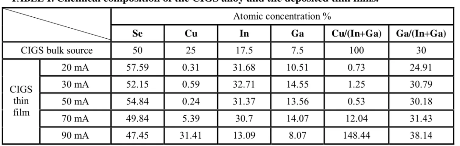
The chemical constituents of the evaporated CIGS films with various electron beam currents were analyzed using an EDX system. The compositions of the as-deposited films were shown in Table I including the constituents of the bulk compound. We found that the composition, especially copper element of thin films have a great change with the different electron beam current. When the beam current was lower than 70 mA, the copper element was hardly evaporated onto thin films. However, as the beam current increased up to 90 mA, the deposited thin film has almost the same composition as that of the bulk. We thought that it may be due to the differences in the melting point and/or the vapor pressures of four elements.
The properties of Cu(In,Ga)Se2 film are affected by
the chemical composition, especially the ratio of Cu/(In+Ga), Ga/(In+Ga). For high efficiency CIGS solar cell, the optimum ratio of Cu/(In+Ga) is about
0.85~0.95, that of Ga/(In+Ga) is about 0.2~0.3. From Table I, the ratio of Ga/(In+Ga) increases with the evaporation current increasing. However, the ratio of Cu/(In+Ga) have a larger fluctuation with the increase of evaporation current. As mentioned above, this is due to the difference of melting point and/or the vapor pressures of the four elements.
Fig. 2.
X-ray diffraction pattern of bulk
Cu(In,Ga)Se
2Figure 2 shows the XRD pattern of bulk CIGS. It shows that the bulk CIGS has chalcopyrite structure. However, the as-deposited CIGS thin films had no peak except Mo (110) peak, which was not shown here. It revealed that the as-deposited films have an amorphous structure in nature. M. Venkatachalam et al. reported that subsequent annealing could make the as-deposited amorphous phased CIGS films be crystallized [3,4]. In this experiment, the annealing processes of the evaporated CIGS films were carried out at the temperature of 550 °C for 1 hour in a Atomic concentration %
Se Cu In Ga Cu/(In+Ga) Ga/(In+Ga)
CIGS bulk source 50 25 17.5 7.5 100 30
20 mA 57.59 0.31 31.68 10.51 0.73 24.91 30 mA 52.15 0.59 32.71 14.55 1.25 30.79 50 mA 54.84 0.24 31.37 13.56 0.53 30.18 70 mA 49.84 5.39 30.7 14.07 12.04 31.43 CIGS thin film 90 mA 47.45 31.41 13.09 8.07 148.44 38.14
P2-100 / Z.-H. Li
• IMID 2009 DIGEST
vacuum of 3×10⁻⁶ torr. Figure 3 shows the XRD
patterns of the annealed films deposited with various evaporation currents. After the subsequent annealing, several peaks begin to appear with variances depending on the electron beam current, which indicates that some grains have been formed in the thin films during the annealing process. However, when the evaporation current was lower than 70 mA, no peaks according the Cu(In,Ga)Se2 crystalline phase
were found. On the other hand, both (InGa)2Se3 and
MoSe2 peaks were obtained. This means that there
was little or no copper element in the films deposited with an evaporation current lower than 70 mA and the copper-deficient or -free film reacted each other to form the (InGa)2Se3 films during the annealing
process [5]. At the same time, some selenium metal is reacted with the Mo layer with resulting in the MoSe2.
For the film deposited with a current of 90 mA, it was observed that the film is crystallized with several peaks of (112), (220)/(224), (312)/(116) which are corresponding to chalcopyrite phase.
Fig. 3. X-ray diffraction pattern of the annealed films at 550 °C
The cross-sectional views for the films annealed at 550 °C for 1 hr under the vacuum were shown in Fig. 4. by using the SEM system. From the Fig. 4, we found no clear crystallites when the evaporation current was lower than 50 mA. For the cases of the films evaporated with a beam current larger than 70 mA, some crystallites began to appear.
Fig. 4. The cross-sectional SEM images of the annealed thin film deposited with different evaporation current: (a) 20 mA, (b) 30 mA, (c) 50 mA, (d) 70 mA, and (e) 90 mA
.
The transmission spectra of the CIGS films, deposited under an evaporation current of 90 mA, were recorded in a range of wavelength of from 500 nm to 1500 nm. From these spectral data, the optical absorption coefficient, α, can be calculated using following formula: [6]
αd=−ln(T) (1)
where, d is the film thickness, T is the transmittance, and α is the absorption coefficient. We can calculate α form equation (1). The optical band gap of thin film,
Eg, can be determined from the absorption coefficient of the films using the following relation: [7]
αhv=[B(hv−Eg)1/2] (2)
where, B is a constant, and Eg is the band gap energy, h is the Plank’s constant, and v is the frequency of the
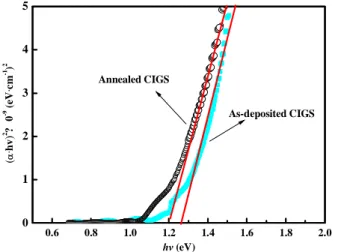
incident photon. Fig. 5 shows the plots of (αhv)2
versus the photon energy hv for the CIGS films deposited under an evaporation current of 90 mA. The
( a ) ( b )
( d )
P2-100 / Z.-H. Li
IMID 2009 DIGEST • band gap Eg is obtained by extrapolating the linear
absorption edge part. When (αhv)2 is zero, the photon
energy is defined as Eg. From Fig. 5, we can obtain
that the Eg of as-deposited CIGS film is 1.27 eV and
that of the CIGS films annealed at 550 °C for 1 hr is 1.20 eV. The difference in the energy band gap may be due to the reduced strains and the reduced dislocation densities in the annealed CIGS thin films [8].
0.6 0.8 1.0 1.2 1.4 1.6 1.8 2.0 0 1 2 3 4 5 ( α ·hv ) 2 ?0 -9 (e V ·cm -1 ) 2 hv (eV) Annealed CIGS As-deposited CIGS
Fig. 5. Plots of (αhv)2 versus hv for CIGS thin films deposited with the evaporation current of 90 mA.
It is known that the band gap of Cu(In,Ga)Se2 film
varies from 1.04 eV to 1.68 eV with different chemical compositions. The band gap versus the element composition, Eg(x), for Cu(In1-xGax)Se2 can
be described as: ) 1 ( ) ( ) ( ) 1 ( ) (x xE CIS xE CGS bx x Eg = − g + g − − (3) where, the Eg(CIS) and the Eg(CGS) are the band gap
of the CuInSe2 and CuGaSe2 respectively. And b is the
bowing coefficient. The value of b is 0.11~0.26 [9,10]. Previous experimental results showed that the solar cell device had the highest efficiency as the band gap of CIGS was 1.2 eV [11]. In this experiment, the band gap of 1.2 eV is obtained for the annealed CIGS film evaporated at a beam current of 90 mA.
4. Summary
Cu(In,Ga)Se2 thin films were formed on Mo coated
soda lime glass using electron-beam evaporation method. The results showed that little or no copper element exist on the deposited thin film when the evaporation current was lower than 70 mA. This may
be due to the lower vapor pressure of copper element. In order to obtain crystallized CIGS films, the as-deposited films were annealed at 550 °C for 1 hour in the vacuum of 3×10⁻⁶ torr. The (112), (220)/(204), and
(312)/(116) peaks corresponding to chalcopyrite structure were observed as the dominating peaks in the annealed film deposited with an evaporation current of 90 mA. The band gap Eg of the annealed
CIGS film was about 1.20 eV.
5. References
1. S. Jackson, B. Barson, R. Rocheleau, and T. Ressell,
Am. Inst. Chem. Eng. J., 33, 711 (1987).
2. T. L. Chu, S. S. Chu, S. C. Lin, and J. Yue, J.
Electrochem. Soc., 131, 2182 (1984).
3. M. Venkatachalam, M. D. Kannan, S. Jayakumar, R. Balasundaraprabhu, A. K. Nandakumar, and N. Muthukumarasamy, Sol. Energy Mater. Sol. Cells,
92, 571 (2008).
4. M. Venkatachalam, M. D. Kannan, S. Jayakumar, R. Balasundaraprabhu, and N. Muthukumarasamy,
Thin Solid Films, 516, 6848 (2008).
5. C. S. Barrett, Structure of Metals: Crystallographic methods, Principles and Data, McGraw-Hill, New York, p.156 (1956).
6. M. Di Giulio, G. Micocci, R. Rella, P. Siciliano, and A. Tepore, Thin Solid Films, 148, 273 (1987). 7. K. V. Madhuri, B. S. Naidu, O. M. Hussain, M.
Eddrief, and C. Julien, Mater. Sci. Eng. B, 86, 165 (2001).
8. N. M. Shah, C. J. Panchal, V. A. Kheraj, J. R. Ray, and M. S. Desai, Solar Energy, 83, 753 (2009). 9. M. I. Alonso, M. Garriga, C. A. Durante Rincón, E.
Hernández and M. León, Appl. Phys. A, 74, 659 (2002).
10. S. H. Wei and A. Zunger, Appl. Phys. Lett., 72, 2011 (1998).
11. L. Stolt, J. Hedstrom, J. Keessier, M. Ruckh, K. O. Velthaus, and H. W. Schock, Appl. Phys. Lett., 62, 597 (1993).