for quantum-dot photovoltaic
cells (
>10%) and their issues with
the measurement of photovoltaic
characteristics
Changsoon Cho
1, Jung Hoon Song
2, Changjo Kim
1, Sohee Jeong
2& Jung-Yong Lee
1 Bandgap tunability and broadband absorption make quantum-dot (QD) photovoltaic cells (PVs) a promising candidate for future solar energy conversion systems. Approaches to improving the electrical properties of the active layer increase efficiency in part. The present study focuses on optical room for enhancement in QD PVs over wide spectrum in the near-infrared (NIR) region. We find that ray-optical light trapping schemes rather than the nanophotonics approach may be the best solution for enhancing broadband QD PVs by suppressing the escape probability of internal photons without spectral dependency. Based on the theoretical study of diverse schemes for various bandgaps, we apply a V-groove structure and a V-groove textured compound parabolic trapper (VCPT) to PbS-based QD PVs along with the measurement issues for PVs with a light scattering layer. The efficiency of the best device is improved from 10.3% to 11.0% (certified to 10.8%) by a V-groove structure despite the possibility of underestimation caused by light scattering in small-area devices (aperture area: 0.0625 cm2). Byminimizing such underestimation, even greater enhancements of 13.6% and 15.6% in short circuit current are demonstrated for finger-type devices (0.167 cm2 without aperture) and large-area devices
(2.10 cm2 with an aperture of 0.350 cm2), respectively, using VCPT.
Low-cost thin-film photovoltaic cells (PVs) have recently shown a dramatic increase in power conversion effi-ciency (PCE). Securing light absorption has been a significant issue for thin-film PVs with a nanometer-scale optical path length limited by their poor charge carrier mobility. Along with the development of novel materials, recent cutting-edge organic and perovskite PVs show a high device absorption of >80% and >90%, respec-tively, for photons within their bandgaps (1.5–2 eV)1–5. For those PVs, nanophotonical approaches adopting metal
nanoparticles6–12 or nanopatterning the interfaces4,5,11–19 have been shown to induce surface plasmon resonance
(SPR) and effectively suppress optical loss at specific less-absorptive wavelength regions such as band-edge4,13,14.
In addition to high absorption, broadening the absorption spectrum is another issue for thin-film PVs to achieve ultrahigh efficiency, whereas IR photons below 1.5 eV account for ~40% of total solar energy20.
Accordingly, quantum-dot (QD) PVs are attracting great attention owing to their bandgap tunability and multiple exciton generation (MEG) effect, possibly breaking the Shockley–Queisser limit21,22 of PCEs23–26. Rapid
advance-ment of QD PVs in recent years has yielded high PCEs comparable to those of organic PVs (OPVs) (>10%)27–32;
PCEs of crystalline silicon (c-Si) PVs (>20%) and the Shockley–Queisser limit (>30%) are the next milestones. QDs used in QD PVs have relatively low bandgaps below 1.5 eV and thus a broad absorption spectrum around the near-IR (NIR) region. However, whereas c-Si PVs typically have a short-circuit current density (Jsc) greater
than 40 mA/cm2 by absorbing light below 1100 nm33,34, J
sc of QD PVs with a similar spectrum range is typically
near or below 30 mA/cm227–30 owing to the low extinction coefficient for NIR, causing broadband optical loss.
The optical properties of low-bandgap QD PVs with a broadband loss have been rarely discussed; a customized
1Graduate School of Energy, Environment, Water, and Sustainability (EEWS), Korea Advanced Institute of Science and Technology (KAIST), Daejeon, 34141, Republic of Korea. 2Korea Institute of Machinery & Materials (KIMM), Daejeon, 34103, Republic of Korea. Correspondence and requests for materials should be addressed to S.J. (email: sjeong@kimm.re.kr) or J.-Y.L. (email: jungyong.lee@kaist.ac.kr)
Received: 29 August 2017 Accepted: 27 November 2017 Published: xx xx xxxx
design rule is needed for light trapping schemes that outperform previous nanophotonical approaches8,35–37 that
target specific wavelengths.
Ray-optical approaches can resolve these optical issues, which have been ignored in thin-film PVs for a while. Previous studies for ray-optical light trapping can be classified into external attachment of textured surfaces12,38–46
or concentrator arrays4,12,47–50 and nonplanar configurations such as double parabolic trapper (DPT)49 or folded
configurations51–54. Although these schemes have been less spotlighted in thin-film PVs with high bandgaps, they
could provide broadband optical gains in QD PVs with low bandgaps if applied appropriately.
The present study aims at maximizing QD PV efficiencies by adopting ray-optical strategies as depicted in Fig. 1. Light trapping for QD PVs are investigated with both theoretical studies and experimental demonstration.
Results and Discussion
In Fig. 2a, a black line represents the PbS QD layer absorption, calculated with a transfer-matrix formalism (TMF)55,56, in the PV structure of indium tin oxide (ITO, 75 nm)/ZnO (50 nm)/PbS QD (270 nm)/Au. The
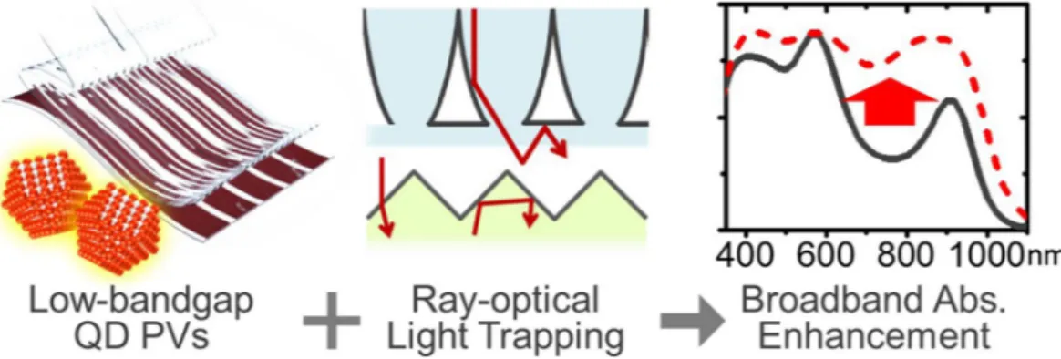
Figure 1. Illustration of ray-optical light trapping for enhancing QD PV absorption.
Figure 2. (a) Active absorption spectra of QD PV with various active layer thicknesses. (b) Active absorption
spectra of nanopatterned QD PV with various periods depicted in the inset. (c) Schematic expression of a PV system composed of an optical component, a spacer, PVs, and a back reflector. (d) Active and parasitic absorption spectra of QD PV according to Pesc at a normal propagation angle.
a height of 150 nm and various periods as shown in the inset. Periodic boundary condition was assumed and the TE-polarized and TM-polarized results were averaged. The absorption is shown to increase near the resonant wavelengths of SPR and the conditions can be simply changed by varying the period. However, there is no struc-ture that is beneficial for all the wavelengths since single SPR is not sufficient to cover the broadband absorption spectrum and even reduces absorption outside the resonant wavelengths. For this reason, we focus on investigat-ing ray-optical approaches with a broadband light trappinvestigat-ing effect rather than nanophotonics for QD PVs.
We generalize typical ray-optical schemes by dividing them into (i) optical components on the top surface; (ii) an optical spacer for ray propagation, usually a glass substrate; (iii) photovoltaic multilayers to absorb photons; and (iv) a back reflector, usually a metal electrode, as shown in Fig. 2c. Contrary to bulk-type PVs, which have a thick active layer as a spacer, the optical spacer and the photovoltaic layers are separated in thin-film PVs, which is why the oblique propagation of light does not necessarily increase the absorption49. Whereas the escape
prob-ability (Pesc)4,13,45 of the internal photons after the first bounce on the photovoltaic layer is almost one for planar
systems, it can be suppressed by proper optical components directing them toward the photovoltaic layers again, as expressed in Fig. 2c. The expected number of multiple bounces becomes Nbounce = 1/Pesc4,13,45.
Figure 2d shows the active absorption spectra of QD PVs for various Pesc values with an assumed fixed
propa-gation angle of zero. The active absorption increases as Pesc decreases and photons bounce more on the active
lay-ers (refer to SI for the calculation method). The maximum active absorption with perfect light trapping (Pesc = 0)
is limited by the ratio of active absorption to the amount of parasitic absorption of nonactive layers such as the metal electrode. If the optical components are made of microstructures, Pesc does not depend on the wavelength,
and a light trapping effect can be uniformly achieved for a broadband spectrum.
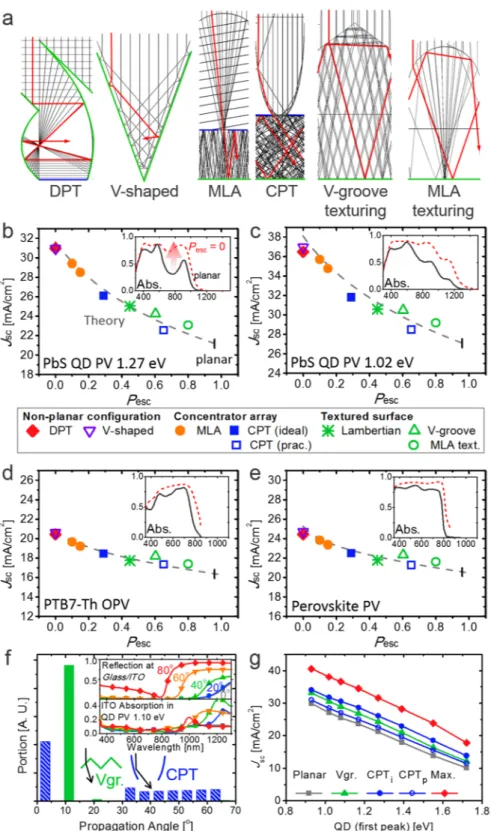
Figure 3a exhibits the ray-traced images for the representative ray-optical schemes that suppress Pesc. DPT,
consisting of two parabolas sharing one focal point, has been proposed as an ideal configuration to realize
Pesc = 049. Folded configurations such as V-shape can also induce high Nbounce by directing incident photons to
the next PV49,51,52,54. Concentrator arrays such as a micro lens array (MLA)47,49 or compound parabolic
trap-per (CPT)4 block the internal photons by implementing blocking mirrors between the entrances. The textured
surfaces with a V-groove39,44,45 or MLA shape38,43 can be considered as a practical scheme to reduce P
esc by total
internal reflection (TIR).
The performance of those schemes for diverse PVs is summarized in Fig. 3b–e. For the gray theoretical lines, short-circuit current densities (Jsc) were obtained by integrating the active absorption spectra for the normal
propagation angle according to Pesc, where the internal quantum efficiency (IQE) was calculated by comparing
the integrated active absorption and experimentally obtained Jsc values (IQE = 1 for QD and perovskite PVs and
0.95 for OPV), ignoring its spectral dependency and MEG for simplicity. The estimated Jsc values of the light
trapping schemes are plotted as a function of Pesc by employing a custom-made multiscale optical simulation4,45,49.
Whereas the DPT and V-shaped (vertex angle of 40°) structures mostly show the lowest Pesc (~0) and the highest Jsc enhancements, their utilization may be limited by their relatively complicated manufacturing processes (i.e.,
nonplanar structures)49. MLA47 and CPT4 with blocking mirrors also show low P
esc and excellent performance.
Whereas MLA suffers from limited angular performance49, CPT uses compound parabolic concentrators (CPCs)
to secure the sufficient acceptance angle with a reasonable Pesc of 0.292. On the other hand, the practically
mod-ified CPT with no blocking mirrors and a truncated CPC height, as described in the previous report4, shows
relatively low performance (Pesc = 0.653). Compared to these schemes, attaching textured films to the top surface
is simpler. A Lambertian scattering surface can realize, as theoretically dictated, Pesc equal to 1/n213,45,61,62. The
V-groove39,45 and MLA38 textured surfaces have relatively higher P
esc; however, their performance was above the
theoretical line because their geometries can also work as an antireflection (AR) structure, reducing the Fresnel reflection loss (~4%) on the substrate4,45.
Although the simulated results for those light trapping schemes are approximately matched with the the-oretical values for given Pesc values, the general tendency was shown to be different for each PV. The
maxi-mum Jsc enhancement for Pesc = 0 is 26.5% for PTB7-Th(poly[[4,8-bis[(2-ethylhexyl)oxy]benzo[1,2-b:4,5-b′]
dithiophene-2,6-diyl][3-fluoro-2-[(2-ethylhexyl)carbonyl]thieno[3,4-b]thiophenediyl]])-based OPV and 22.8% for perovskite PV, and it becomes relatively larger for QD PVs (40.6% for 1.02 eV and 49.3% for 1.27 eV) as greater room for enhancement exists as shown in the insets of Fig. 3b–e.
Notably, for QD PVs with low bandgaps, the performance of DPT, V-shaped, CPT, and Lambertian structures is shown to be lower than the theoretical expectation from their Pesc values. Those schemes have a relatively high
level of light scattering compared to schemes such as MLA and V-groove texturing as shown in Fig. 3f. Although ITO is a transparent material for visible light, it becomes metallic for NIR photons as shown in the refractive indi-ces of Figure S1. Therefore, surface reflection and parasitic absorption loss of ITO4,13,45 become significant at long
Figure 3. (a) Ray-traced images of the unit structure of periodic arrays for the various light trapping schemes.
Green and blue lines indicate PVs and metal mirrors, respectively38,45,49. (b–e) Simulated values for the schemes
of (a) and calculated Jsc values (dashed line) according to Pesc of (b) QD PV with PbS 1.27 eV, (c) QD PV with
PbS 1.02 eV, (d) PTB7-Th OPV, and (e) perovskite PV. (f) Distribution of the photon propagation angle inside the substrate after passing V-groove texturing (green) and CPT (blue). (inset: Fresnel reflection ratio at the interface between glass and ITO (above) and parasitic absorption of ITO in a full device using QD 1.10 eV with various propagation angles). (g) Calculated Jsc values of QD PVs with various bandgaps and schemes of
of the cell area. However, although this system is considered as a standard for planar PVs, it is possible to underes-timate the photocurrent where a scattering layer is embedded on the topside because scattered light may deviate from the cell area. For that reason, many previous studies4,38,40,43,45 for ray-optical light trapping structures have
chosen measurement without apertures, but such measurement issues have been rarely examined.
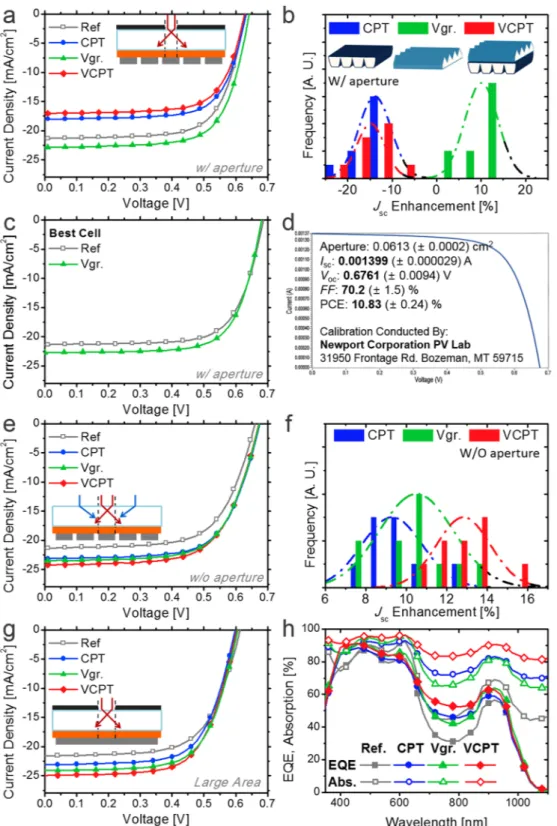
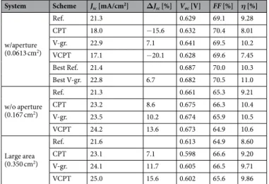
Figure 4a and Table 1 show the J–V characteristics of the QD PV with and without light trapping schemes in the standard measurement system. An aperture with a defined illumination area of 0.0625 cm2 was applied for
the device with 5 cells of 0.12–0.17 cm2 size in parallel as shown in Figure S2a. The PCE of the control device
was 9.28% with a spectral mismatch factor of 0.930. Whereas the best PCE of 10.2% (Jsc 7.1% ↑) was achieved
with the V-groove textured film, the Jsc values and PCEs for CPT and VCPT devices were even much lower
than the reference. Such current reduction mainly results from the optical loss in the measurement setup using apertures. Whereas light through the aperture is fully illuminated inside the cell area for flat control devices, that with scattering surfaces may deviate from the cell and be lost as depicted in the inset of Fig. 4a. Compared to CPT and VCPT with high-level scattering angles, such optical loss was relatively small for V-groove tex-turing, so the average Jsc enhancements of 10.1% could be achieved from repeated measurements as shown in
Fig. 4b.
In this study, we used only the middle cell of the 5 fingers on each device to secure the periodic boundary condition, which will be described in Figs 4e and S2a. On the other hand, along with the cell-by-cell deviation of the efficiency, the highest efficiency greater than 10% was observed in an edge-side cell of one device. By attaching V-groove textured film, the efficiency of the best cell was improved from 10.3% to 11.0% (Jsc 6.7% ↑) as shown
in Fig. 4c. The result shows that the light trapping effect can be consistently achieved even for highly efficient devices. Our best device was certified by Newport Corporation, and the PCE was 10.83(±0.24)% with V-groove texturing as shown in Figs 4d, and S5. During the certification, the V-groove textured film may have been con-taminated by repeated processes of attaching and detaching. We noticed that the PCE of the retrieved device was recovered by replacing the film with a fresh one that had 3% increased Jsc.
Underestimation of the light trapping effect can be minimized by full illumination on finger-type PVs without apertures as depicted in the inset of Figs 4e and S2a–d. In that case, only the middle cell among 5 fingers can be measured to assume the periodic boundary condition (PBC), so the amount of light scattered from the outside to the cell (blue) is considered to be the same as that scattered from the cell to the outside (red), ignoring the optical loss through the gaps between the cells. We characterized the PV performance in that system. We used an effec-tive cell area, which is calculated by dividing the total photocurrent by Jsc from the same device with an aperture,
rather than the geometrical cell area, to exclude the possible overestimation factors such as underestimation of the cell area or charge diffusion from outside4. In that system with the same device used in Fig. 4a, PCE was improved
from 9.21% to 10.4% (Jsc 8.5% ↑), 10.5% (Jsc 10.2% ↑), and 10.6% (Jsc 13.6% ↑) by attaching CPT, V-groove
tex-turing, and VCPT films, respectively, as shown in Fig. 4e and Table 1. Figure 4f clearly shows that the highest Jsc
enhancement is achieved by VCPT (12.8% on average) when the aperture is removed, whereas that for V-groove texturing (10.5% on average) is not much different from that with the aperture.
Obviously, the most accurate evaluation of the light trapping effect can be achieved in devices with large areas and a sufficient marginal distance (>5 mm) as depicted in the inset of Figs 4g and S2e–h. Apparently, the large-area configuration is closer to the practical outdoor modules in terms of optics. As shown in Fig. 4g and Table 1, the PCE of a large-area (2.10 cm2) QD PV with an aperture of 0.350 cm2 was improved from 8.60% to
9.20% (Jsc 7.1% ↑), 9.71% (Jsc 11.7% ↑), and 9.86% (Jsc 15.6% ↑) by adopting CPT, V-groove texturing, and VCPT,
respectively. Conversely, the Jsc enhancements of finger-type cells without an aperture (Fig. 4e,f) are 1–2% lower.
Whereas the small optical loss may result from the 1 mm gaps between the 3 mm fingers (Figure S2a), the meas-ured enhancements are much closer to those of the practical large-area devices than those of small-area devices with apertures (Fig. 4a,b), supporting the validity of our method.
The fabrication of large-area devices enables achievement of the spectral responses without optical loss4.
The measured external quantum efficiencies (EQEs) and total device absorption (=1 − reflection) are shown in Fig. 4h. Each value was measured in both polarizations to remove the polarizing effect of the light source. The EQE was enhanced by adopting light trapping schemes over the whole spectral range, but the enhancements were not uniform owing to the spectral characteristics as discussed in Fig. 3f. EQE data for the lower-bandgap (1.17 eV) QD PV are shown in Figure S3 to evaluate the spectral influence of light trapping schemes.
Conclusion
Optical schemes including plasmonic nanostructures, nonplanar configurations (DPT and V-shaped), concentrator arrays (MLA and CPT), and textured surfaces (Lambertian, V-groove, and MLA) have been
studied to improve QD PV efficiency. The certified PCE of the best cell was improved from 10.3% to 11.0% by light trapping, and enhancement greater than 15% was proved to be possible for practical large-area devices with VCPT.
Figure 4. (a,e) J–V characteristics and (b,f) Jsc enhancements of QD PV with light trapping schemes (a,b) with
and (e,f) without aperture. (c) J–V characteristics of the best cell with aperture with and without V-groove texturing. (d) Certified data for V-groove textured device of (c) (Newport Co.). (g) J–V characteristics of large-area QD PV with light trapping schemes and aperture. (h) EQE and absorption spectra of PV in (g). (EQE-integrated Jsc = 22.6 (ref.), 24.8 (CPT), 25.4 (Vgr.), and 26.3 (VCPT) mA/cm2, respectively).
Materials and Methods
The performance of the ray-optical schemes was evaluated by a custom-made multiscale simulation, which was used for our previous studies4,40,45,49. Two hundred rays with a full spectrum were traced for each unit structure,
and the PBC was applied.
For device fabrication, ZnO synthesized by the sol-gel method was spin-coated onto ITO substrates at 3000 rpm for 30 s and annealed at 200 °C for 10 min. PbS QD films (270 nm) were deposited using a layer-by-layer (LBL) spin-coating process on the ZnO substrate at 2500 rpm as described in previous reports30,31. For the LBL spin-coating process, solid-state ligand exchange was performed using 7 mg mL−1 of
1-ethyl-3-methylimidazolium iodide (EMII) solutions (in methanol) and 0.01% ethanedithiol (EDT) solutions (in acetonitrile) on the surface of the PbS films. After the LBL spin-coating process, the sample was stored in nitrogen environment for 12 h, and post-annealing was performed at 100 °C for 10 min. Finally, Au (70 nm) layers were deposited by thermal evaporation. J–V characteristics of PVs were obtained under 1 sun illumination with the AM 1.5 G spectrum using a K201 LAB55 (McScience, Korea) solar simulator. J–V curves were swept in the reverse direction, and the hysteresis was shown to be negligible (<1%). A spectral mismatch factor of 0.93 was applied. Finger-type devices with a cell area of 0.12–0.17 cm2 and aperture of 0.0613 cm2 were used for the
exper-iments. All light-trapped devices were measured immediately after the reference devices to fairly compare the Jsc
enhancement. To secure a sufficient number of data points for Jsc enhancements in Fig. 4b,f, old devices, which
have the same structure and possibly include degradation, were also used for the experiment.
The datasets generated during and/or analysed during the current study are available from the corresponding author on reasonable request.
References
1. Tan, H. R. et al. Efficient and stable solution-processed planar perovskite solar cells via contact passivation. Science 355, 722–726 (2017). 2. Yang, W. S. et al. High-performance photovoltaic perovskite layers fabricated through intramolecular exchange. Science 348,
1234–1237 (2015).
3. Shin, S. S. et al. Colloidally prepared La-doped BaSnO3 electrodes for efficient, photostable perovskite solar cells. Science 356, 167–171 (2017).
4. Cho, C. et al. Toward Perfect Light Trapping in Thin-Film Photovoltaic Cells: Full Utilization of the Dual Characteristics of Light.
Adv. Optical Mater. 3, 1697–1702 (2015).
5. Jeong, S. et al. Nanoimprinting-Induced Nanomorphological Transition in Polymer Solar Cells: Enhanced Electrical and Optical Performance. Acs Nano 9, 2773–2782 (2015).
6. Baek, S. W. et al. Plasmonic Forward Scattering Effect in Organic Solar Cells: A Powerful Optical Engineering Method. Sci. Rep. 3, 7 (2013).
7. Baek, S.-W. et al. Au@Ag Core-Shell Nanocubes for Efficient Plasmonic Light Scattering Effect in Low Bandgap Organic Solar Cells.
Acs Nano 8, 3302–3312 (2014).
8. Baek, S. W. et al. A Resonance-Shifting Hybrid n-Type Layer for Boosting Near-Infrared Response in Highly Efficient Colloidal Quantum Dots Solar Cells. Adv. Mater. 27, 8102–8108 (2015).
9. Baek, S. W. et al. Plasmonic Forward Scattering Effect in Organic Solar Cells: A Powerful Optical Engineering Method. Sci. Rep. 3, 1726–1732 (2013).
10. Lee, J. Y. & Peumans, P. The origin of enhanced optical absorption in solar cells with metal nanoparticles embedded in the active layer. Opt. Express 18, 10078–10087 (2010).
11. Atwater, H. A. & Polman, A. Plasmonics for improved photovoltaic devices. Nat. Mater. 9, 205–213 (2010). 12. Ou, Q. D., Li, Y. Q. & Tang, J. X. Light Manipulation in Organic Photovoltaics. Adv. Sci. 3, 1600123–1600147 (2016).
13. Cho, C., Jeong, S. & Lee, J.-Y. Optical study of thin-film photovoltaic cells with apparent optical path length. J. Opt. 18, 094001–094008 (2016).
14. Abass, A., Shen, H. H., Bienstman, P. & Maes, B. Angle insensitive enhancement of organic solar cells using metallic gratings. J. Appl.
Phys. 109, 023111–023117 (2011).
15. Min, C. J. et al. Enhancement of optical absorption in thin-film organic solar cells through the excitation of plasmonic modes in metallic gratings. Appl. Phys. Lett. 96, 133302–133304 (2010).
16. Kang, D. J. et al. Efficient light trapping in inverted polymer solar cells by a randomly nanostructured electrode using monodispersed polymer nanoparticles. Nanoscale 5, 1858–1863 (2013).
Large area (0.350 cm2) Ref. 21.6 0.613 64.9 8.60 CPT 23.1 7.1 0.598 66.6 9.20 V-gr. 24.1 11.7 0.605 66.5 9.71 VCPT 25.0 15.6 0.602 65.6 9.86
17. Kim, J. B. et al. Wrinkles and deep folds as photonic structures in photovoltaics. Nat. Photonics 6, 327–332 (2012). 18. Ko, D. H. et al. Photonic Crystal Geometry for Organic Solar Cells. Nano Lett. 9, 2742–2746 (2009).
19. An, C. J. et al. Highly Efficient Top-Illuminated Flexible Polymer Solar Cells with a Nanopatterned 3D Microresonant Cavity. Small
10, 1278–1283 (2014).
20. Otanicar, T. P., Chowdhury, I., Prasher, R. & Phelan, P. E. Band-Gap Tuned Direct Absorption for a Hybrid Concentrating Solar Photovoltaic/Thermal System. Journal of Solar Energy Engineering-Transactions of the Asme 133, 041014–041020 (2011). 21. Shockley, W. & Queisser, H. J. Detailed Balance Limit of Efficiency of p‐n Junction Solar Cells. J. Appl. Phys. 32, 510–519 (1961). 22. Ruhle, S. Tabulated values of the Shockley-Queisser limit for single junction solar cells. Solar Energy 130, 139–147 (2016). 23. Nozik, A. J. Quantum dot solar cells. Physica E-Low-Dimensional Systems & Nanostructures 14, 115–120 (2002).
24. Ellingson, R. J. et al. Highly efficient multiple exciton generation in colloidal PbSe and PbS quantum dots. Nano Lett. 5, 865–871 (2005).
25. Semonin, O. E. et al. Peak External Photocurrent Quantum Efficiency Exceeding 100% via MEG in a Quantum Dot Solar Cell.
Science 334, 1530–1533 (2011).
26. Yan, Y. et al. Multiple exciton generation for photoelectrochemical hydrogen evolution reactions with quantum yields exceeding 100%. 2, 17052–17058 (2017).
27. Lan, X. Z. et al. 10.6% Certified Colloidal Quantum Dot Solar Cells via Solvent Polarity-Engineered Halide Passivation. Nano Lett.
16, 4630–4634 (2016).
28. Liu, M. X. et al. Hybrid organic-inorganic inks flatten the energy landscape in colloidal quantum dot solids. Nat. Mater. 16, 258–263 (2017).
29. Sun, B. et al. Pseudohalide-Exchanged Quantum Dot Solids Achieve Record Quantum Efficiency in Infrared Photovoltaics. Adv.
Mater. 1700749-1700753 (2017).
30. Song, J. H., Choi, H., Kim, Y.-h. & Jeong, S. High Performance Colloidal Quantum Dot Photovoltaics by Controlling Protic Solvents in Ligand Exchange. Adv. Energy Mater. 1700301–1700306 (2017).
31. Cao, Y. M., Stavrinadis, A., Lasanta, T., So, D. & Konstantatos, G. The role of surface passivation for efficient and photostable PbS quantum dot solar cells. Nature Energy 1 (2016).
32. Stavrinadis, A., Pradhan, S., Papagiorgis, P., Itskos, G. & Konstantatos, G. Suppressing Deep Traps in PbS Colloidal Quantum Dots via Facile Iodide Substitutional Doping for Solar Cells with Efficiency > 10%. Acs Energy Letters 2, 739–744 (2017).
33. Zhao, J. H., Wang, A. H. & Green, M. A. 24 center dot 5% efficiency silicon PERT cells on MCZ substrates and 24 center dot 7% efficiency PERL cells on FZ substrates. Prog. Photovoltaics 7, 471–474 (1999).
34. Zhao, J. H., Wang, A. H. & Green, M. A. High-efficiency PERL and PERT silicon solar cells on FZ and MCZ substrates. Sol. Energy
Mater. Sol. Cells 65, 429–435 (2001).
35. de Arquer, F. P. G., Beck, F. J., Bernechea, M. & Konstantatos, G. Plasmonic light trapping leads to responsivity increase in colloidal quantum dot photodetectors. Appl. Phys. Lett. 100, 043101–043104 (2012).
36. Miller, C. W., Fu, Y. L. & Lopez, R. Enhancing energy absorption in quantum dot solar cells via periodic light-trapping microstructures. J. Opt. 18, 094002–094008 (2016).
37. Zhang, X. L. & Johansson, E. M. J. Utilizing light trapping interference effects in microcavity structured colloidal quantum dot solar cells: A combined theoretical and experimental approach. Nano Energy 28, 71–77 (2016).
38. Myers, J. D. et al. A universal optical approach to enhancing efficiency of organic-based photovoltaic devices. Energy Environ. Sci. 5, 6900–6904 (2012).
39. Esiner, S., Bus, T., Wienk, M. M., Hermans, K. & Janssen, R. A. J. Quantification and Validation of the Efficiency Enhancement Reached by Application of a Retroreflective Light Trapping Texture on a Polymer Solar Cell. Adv. Energy Mater. 3, 1013–1017 (2013). 40. Kang, J., Cho, C. & Lee, J.-Y. Design of asymmetrically textured structure for efficient light trapping in building-integrated
photovoltaics. Org. Electron. 26, 61–65 (2015).
41. Yun, J. et al. Light trapping in bendable organic solar cells using silica nanoparticle arrays. Energy Environ. Sci. 8, 932–940 (2015). 42. Chen, J. D. et al. Enhanced Light Harvesting in Organic Solar Cells Featuring a Biomimetic Active Layer and a Self-Cleaning
AntireflectiveCoating. Adv. Energy Mater. 4, 1301777–1301784 (2014).
43. Lampande, R., Kim, G. W., Park, M. J., Kang, B. Y. & Kwon, J. H. Efficient light harvesting in inverted polymer solar cells using polymeric 2D-microstructures. Sol. Energy Mater. Sol. Cells 151, 162–168 (2016).
44. Borse, K. et al. Efficient light trapping and interface engineering for performance enhancement in PTB7-Th: PC70BM organic solar cells. Org. Electron. 41, 280–286 (2017).
45. Cho, C. et al. Random and V-groove texturing for efficient light trapping in organic photovoltaic cells. Sol. Energy Mater. Sol. Cells
115, 36–41 (2013).
46. Lee, H. S. et al. Effects of Backbone Planarity and Tightly Packed Alkyl Chains in the Donor-Acceptor Polymers for High Photostability. Macromolecules 49, 7844–7856 (2016).
47. Tvingstedt, K., Dal Zilio, S., Inganas, O. & Tormen, M. Trapping light with micro lenses in thin film organic photovoltaic cells. Opt.
Express 16, 21608–21615 (2008).
48. Peumans, P., Bulovic, V. & Forrest, S. R. Efficient photon harvesting at high optical intensities in ultrathin organic double-heterostructure photovoltaic diodes. Appl. Phys. Lett. 76, 2650–2652 (2000).
49. Cho, C. & Lee, J. Y. Multi-scale and angular analysis of ray-optical light trapping schemes in thin-film solar cells: Micro lens array, V-shaped configuration, and double parabolic trapper. Opt. Express 21, A276–A284 (2013).
50. Lee, W. et al. Self-Organization of Polymer Additive, Poly(2-vinylpyridine) via One-Step Solution Processing to Enhance the Efficiency and Stability of Polymer Solar Cells. Adv. Energy Mater. 1602812–1602820 (2017).
51. Tvingstedt, K., Andersson, V., Zhang, F. & Inganas, O. Folded reflective tandem polymer solar cell doubles efficiency. Appl. Phys. Lett.
91, 123514–123516 (2007).
52. Rim, S. B., Zhao, S., Scully, S. R., McGehee, M. D. & Peumans, P. An effective light trapping configuration for thin-film solar cells.
Appl. Phys. Lett. 91, 243501–243503 (2007).
53. Niggemann, M. et al. Functional microprism substrate for organic solar cells. Thin Solid Films 511, 628–633 (2006). 54. Koleilat, G. I. et al. Folded-Light-Path Colloidal Quantum Dot Solar Cells. Sci. Rep. 3 (2013).
55. Pettersson, L. A. A., Roman, L. S. & Inganas, O. Modeling photocurrent action spectra of photovoltaic devices based on organic thin films. J. Appl. Phys. 86, 487–496 (1999).
56. Peumans, P., Yakimov, A. & Forrest, S. R. Small molecular weight organic thin-film photodetectors and solar cells. J. Appl. Phys. 93, 3693–3723 (2003).
57. Pattantyus-Abraham, A. G. et al. Depleted-Heterojunction Colloidal Quantum Dot Solar Cells. Acs Nano 4, 3374–3380 (2010). 58. Zhitomirsky, D., Voznyy, O., Hoogland, S. & Sargent, E. H. Measuring Charge Carrier Diffusion in Coupled Colloidal Quantum Dot
Solids. Acs Nano 7, 5282–5290 (2013).
59. Jeong, Y. J. et al. Charge Transport Characterization of PbS Quantum Dot Solids for High Efficiency Solar Cells. Journal of the Optical
Society of Korea 19, 272–276 (2015).
60. Jin, J. The Finite Element Method in Electromagnetics. (Wiley, 2002).
61. Campbell, P. & Green, M. A. Light Trapping Properties Of Pyramidally Textured Surfaces. J. Appl. Phys. 62, 243–249 (1987). 62. Yablonovitch, E. Statistical Ray Optics. Journal of the Optical Society of America 72, 899–907 (1982).
Competing Interests: The authors declare that they have no competing interests.
Publisher's note: Springer Nature remains neutral with regard to jurisdictional claims in published maps and
institutional affiliations.
Open Access This article is licensed under a Creative Commons Attribution 4.0 International
License, which permits use, sharing, adaptation, distribution and reproduction in any medium or format, as long as you give appropriate credit to the original author(s) and the source, provide a link to the Cre-ative Commons license, and indicate if changes were made. The images or other third party material in this article are included in the article’s Creative Commons license, unless indicated otherwise in a credit line to the material. If material is not included in the article’s Creative Commons license and your intended use is not per-mitted by statutory regulation or exceeds the perper-mitted use, you will need to obtain permission directly from the copyright holder. To view a copy of this license, visit http://creativecommons.org/licenses/by/4.0/.