12-1 / I. Han
IMID 2009 DIGEST •
Abstract
The cost effective structures and materials for the carbon nanotube (CNT) back light unit (BLU) are proposed. Simplified device structures and related electron emitter materials are prepared. CNT emitters were screen printed or remotely mounted on the back plate, and this enabled less than two photo patterning steps. Besides the cost benefits, operating voltage was dramatically decreased and higher current density was obtained
1. Introduction
We demonstrated the improved image qualities of LCD-TV using CNT-BLU. Although there are still several technical huddles to overcome to be commercialized as like high voltage stability, power consumption, maximum brightness, etc, we guess that those huddles can be overcome through the continuous improvement of current technologies. However, the cost of CNT-BLU strongly depends on the device structure and process steps also depending on the material properties. The current lamp cost and overall BLU cost including optical sheets are estimated about 120 US dollars and 240 US dollars respectively for 40 inch LCD display in general. [1] We have been searching for the innovative materials and structures to minimize process steps for CNT-BLU fabrication. The simplest structure of CNT-CNT-BLU is remote gate one. This structure was originally proposed in the CNT-FED and mesh gate is mounted above the back plate with a few hundred microns gap between CNTs and mesh gate. The mesh gate acted as an extraction electrode in CNT-BLU while it was a focus electrode in CNT-FED. Moreover the remove of activation process for the emitter formations helps the fabrication process simple. Many researchers have tried to get low operation voltage with enough emission uniformity without activation process. However, those efforts showed not enough properties to be used for commercial applications. Here the
feasibility studies about the activation-free CNT emitters and related devices structures are described.
ITEM performance Related Target
Structure Cost Simplest Reliability < 50,000 hr Brightness > 15,000 cd/m2 High voltage stability Power > 40 lm/W Light weight < 8 kg Glass thickness Thickness < 3 mm
2. Experimental
The structures and basic formulation of CNT paste were reported before. [2] The CNT BLU has emitters, anode screen, and vacuum gap between them. Brightness uniformity can be improved by optimizing the emitter array design and cathodoluminescence scattering structure. The direct growth of CNTs on conducting fibers was performed with the same process described previously. [3]
3. Results and discussion
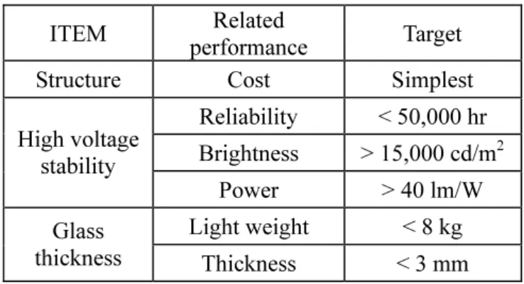
We controlled the formulation of CNT paste to generate cracks after the screen printing process. The 50 um pitch line cracks were achieved and CNTs were exposed into the air. Some CNTs showed tip ends while most of them were hanging between paste walls. The density of cracks strongly depends on the ingredients of paste. The field emission measurement data demonstrated that the current density was 100 times higher than that of CNT pastes fabricated
Table 1. Requirements for CNT-BLU
Cost effective CNT-BLU
In Taek Han
1, Yong Cheol Kim
1, Ha Jin Kim
1, Young Whan Kim
1and Jong
Min Kim
21Materials Research Lab., SAIT, Samsung Electronics, Yong-In, Kyoung-ki 446-712, Korea
TEL:82-2-280-9342, e-mail:
[email protected]
2Frontier Research Lab., SAIT, Samsung Electronics, Yong-In, Kyoung-ki 446-712, Korea
12-1 / I. Han
• IMID 2009 DIGEST
through tape activation process. It is thought that the increase of emission site density and the decrease of electrical field screening effect played an important role for such high current density.
Fig. 1. (a) Self-cracked morphology of CNT paste and (b) CNTs hanging on a cliff.
Fig. 2. Field emission curve and electric field distribution modeling image.
Second concept is to make an assembled CNT-BLU from CNT emitter to gate electrode like a lego block. To realize this, CNTs were grown on a fibrous material with chemical vapor deposition (CVD) process. The bundles of CNT coated conductive fiber
were placed on the cathode electrode, and mesh gate placed on the gate insulator. This structure showed very low gate operating voltage. The curled electric field along the conductive fiber decreased operation voltage. However, the development of precise mounting technique of emitter fibers and mesh gates is required to accomplish this concept as a real device.
Fig. 3. (a) CNT coated conductive fiber and (b) a schematic of CNT-BLU cathode.
1 2 3 4 5 6 0 100 200 300 400 500 0.0 0.5 1.0 1.5 2.0 2.5 -44 -42 -40 -38 -36 -34 ln ( I/E 2) 1/E (x 10-6) CNT on flat Si CNT on CF Em iss ion C urr en t ( μ A) Applied Field (V/μm)
Fig. 2. V-I curve with a light emission image on green phosphor.
Although the proof of device concept and basic operation properties were confirmed, there are many huddles to overcome before the commercialization of the CNT-BLU as like the improvement of lumen efficacy and high voltage reliability. Most of all, reduction of the manufacturing cost is the key success factor of these devices. It is difficult to calculate exactly the cost due to the many variables of the devices structures and process. However it is clear that as we decrease the number of process steps as like activation process, the cost will be comparable with emerging back lighting units.
4. Summary
The cost effective structures and materials for the carbon nanotube (CNT) back light unit (BLU) are proposed. Simplified device structures and related electron emitter materials are prepared. CNT emitters
12-1 / I. Han
IMID 2009 DIGEST •
were screen printed or remotely mounted on the back plate, and this enabled less than two photo patterning steps. Besides the cost benefits, operating voltage was dramatically decreased and higher current density was obtained
5. References
1. 2008 LCD Backlight Report: Including LCD-TV, Monitor & Notebook PC Displays - An Opportunity Analysis, Insight Media (2008). 2. Y. Kim, Nanotechnology, 20 pp095203-29 (2009). 3. International Symposium on Discharges and
Electrical Insulation in Vacuum, 2, Sept. 2006 pp888 - 889