2-4 / W. S. Moon
IMID 2009 DIGEST • Keywords: dielectric constant, dielectric layer, efficacy
Abstract
We investigated the effect of relative dielectric constant of front dielectric layer on the efficacy of plasma display panel. Dielectric materials with relative dielectric constant of around 6 and 7 were developed. When the front dielectric layer had a low relative dielectric constant, power consumption decreased more than luminance did. And it led to efficacy enhancement. However, the minimum sustain voltage increased.
1. Introduction
With growing severe competition between various technologies for large size, flat panel TV, high efficacy is one of the key requirements for PDP to remain competitive in the market. Growing awareness of energy consumption is another factor that drives TVs to be more energy-efficient. Design of electrodes, cell structure and driving schemes have been improved for better performance in efficacy [1, 2]. Material development of the enhancement of efficacy is mainly focused on the protective layer and phosphors which have direct effect on the discharge phenomenon and visible light generation. With increasing concern on the environment, however, lead-free dielectric materials are tested and adopted for the PDP manufacturing even though lead (Pb) based dielectric materials have been used for years due to their good thermal and electrical characteristics and low cost [3]. Transparent dielectric material is used in the front plate of PDP and is closely related to the capacitance of a panel and visible light transmission which affect the efficacy of a panel. For designing new dielectric material, it is important to know how the material influences on the performance of PDP. In this study, the effect of dielectric property of front dielectric layer on the efficacy of plasma display panel was investigated.
2. Experimental
Glass powders of ZnO-SiO2-B2O3 system with
some alkaline and alkaline-earth metal oxide were prepared through melting, crushing and milling process. For use in the manufacturing process of a PDP, the glass powders were mixed with organic solvents and binders, and were made into green sheets. The thermal characteristics of each glass powder were analyzed by TMA (Thermal Mechanical Analyzer, Netzsch TMA402). The viscosity at high temperature was measured by high temperature viscometer (HKL). The relative dielectric constants were determined by HP4194A impedance analyzer at 1Mz.
50” commercial grade panels (HD) were manufactured with those dielectric materials as the front dielectric layer. Other parts such as ITO and bus electrodes, barrier ribs, reflective layer, phosphors and protective layer were prepared with commercial materials and the dimensions for each part were kept the same as those of commercial panel. The performances such as the luminance, power consumption were evaluated at normal operating conditions. ICCD was used to monitor the formation and propagation of a discharge in a cell.
3. Results and discussion
Several kinds of dielectric materials were developed and tested with their basic properties such as transmittance, glass transition temperature and softening temperature. The final ones had relative dielectric constants around 6 and 7. Glass powders of ZnO-SiO2-B2O3 system generally have relative
dielectric constants lower than 10 due to their lack of lead. Table 1 shows the thermal characteristics of resulting glass powders and conventionally used one.
Effect of the Front Dielectric Layer on the Efficacy of the Plasma Display Panel
Won Seok Moon1*, Jin Mok Oh1, Byung Hwa Seo1, Sung Wook Lee1, Na Mi
Byun1, Yun Hui Cho2, Byung Gil Ryu1, Sung Tae Kim1
1Display Research Lab., LG Electronics Inc., Seoul, Korea
Tel.:82-2-526-4851, E-mail: [email protected]
2-4 / W. S. Moon
• IMID 2009 DIGEST
TABLE 1. Electrical and thermal properties of each dielectric material
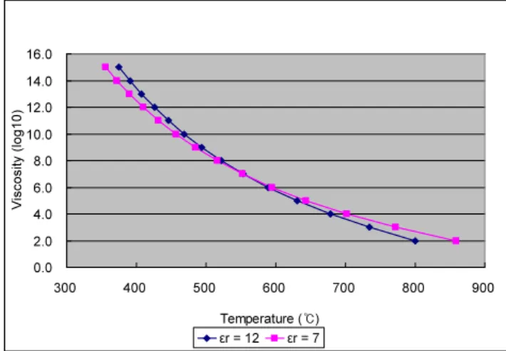
A B Conventional Relative dielectric constant, εr (-) ~7 ~6 ~12 Glass transition temperature, Tg (degC) 490 478 494 Dilatometric softening point, Tdsp (degC) 539 524 533 Coefficient of thermal expansion, CTE (1/K) 87 87 84 New materials should show similar thermal behaviour to that of previous one for them to be used in the manufacturing process without significant process changes, especially firing temperature. Figure 1 shows the change of viscosity of developed glass powder (A) and conventional one with temperature. They had almost the same viscosity in the temperature range of 550 ~ 600 degC where the firing of a transparent dielectric layer is processed.
0.0 2.0 4.0 6.0 8.0 10.0 12.0 14.0 16.0 300 400 500 600 700 800 900 Temperature (℃) V is co si ty (l og 10 ) εr = 12 εr = 7
Fig. 1. Comparison of the viscosity of glass powders with temperature
The front dielectric layer functions as a capacitor and the capacitance can be divided into electrostatic and electrodynamic ones [4]. The electrostatic capacitance is related to the reactive power and voltage loss in the dielectric materials. The reactive power loss can be decreased when a thinner front dielectric layer is used [5]. The electrodynamic capacitance is related to the discharge and can be expressed as follows
d A
C=εr (1)
where εr is the relative dielectric constant, A is the
area of the electrodes and d is the thickness of the dielectric layer.
When the design of the electrodes is the same, the electrodynamic capacitance is determined by the ratio of the relative dielectric constant and the thickness of the front dielectric layer. In this study, the change of the thickness was negligible compared to that of relative dielectric constant. Therefore, the electrodynamic capacitance is governed mostly by the dielectric property of the materials.
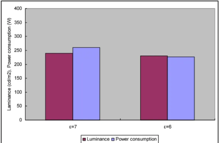
The luminance and the power consumption of the panels with different dielectric materials were compared in Figure 2 and 3. As the relative dielectric constant becomes lower, both the luminance and the power consumption decreased. In both cases, the decrease in power consumption surpassed that of the luminance. Consequently, the efficacy was enhanced with lower relative dielectric constants.
Differences in the transmittance of the dielectric materials and thickness of the front dielectric layer might affect the transmittance of the front dielectric layer and the luminance of the panel. To exclude this effect, specific performance index (SPI) efficacy [4] which takes the reflection of a panel into account was calculated and shown in Table 2. The SPI efficacy for each panel shows that the low relative dielectric constant of a front dielectric layer favours high efficacy. This coincides with the report of Oversluizen and Dekker who showed that panel with small capacitance produced high efficacy [6].
0 50 100 150 200 250 300 350 400 ε=12 ε=7 La mi na nc e ( cd /m 2), P ow er co ns um pti on (W )
Luminance Power consumption
Fig. 2. Comparison of the performance of panel with dielectric materials of εr =12 and εr =7
2-4 / W. S. Moon IMID 2009 DIGEST • 0 50 100 150 200 250 300 350 400 ε=7 ε=6 La mi na nc e ( cd /m 2), P ow er co ns um pti on (W )
Luminance Power consumption
Fig. 3. Comparison of the performance of panel with dielectric materials of εr =7 and εr =6
(thickness 24um for both panels)
TABLE 2. Comparison of SPI efficacy between different front dielectric materials
Case 1 Case 2 Relative dielectric
constant, εr 12 7 7 6
SPI efficacy 3.23 3.36 4.00 4.12 Table 3 shows the ratio of the relative dielectric constant and the thickness of the front dielectric layer and minimum sustain voltage for each case. As the electrodynamic capacitance became smaller, the minimum sustain voltage increased. This can be attributed to the smaller amount of wall charges for smaller capacitance. With relative dielectric constant of 6, the minimum sustain voltage was the largest, 202V. The reactive power loss is proportional to the square of sustain voltage. Hence, the increase of sustain voltage should be kept small. Thickness of around 20um is required for εr = 6 material to have
equivalent εr / d ratio with εr = 7. This might cause
problems in reliability due to reduced thickness uniformity and increased possibility of electrical breakdown. Therefore, further study is needed.
TABLE 3. Relative dielectric constants, thickness and minimum sustain voltage of each panel
Case 1 Case 2 Relative dielectric constant, εr 12 7 7 6 Thickness, d (um) 28 25 24 24 εr / d 0.43 0.28 0.29 0.25 Vs,min (V) 174 184 188 202
Figure 4 shows a series of ICCD images for different εr / d. The panel which had lower
electrodynamic capacitance appeared to have a shorter discharge duration. The propagation of discharge in a cell was calculated from ICCD data for each panel, and the results are shown in Figure 5. It shows that the discharge proceeded at a faster speed for panel with lower relative dielectric constant. This can be explained by the decrease in the electrodynamic capacitance which should be filled by the discharge. Oversluizen and Dekker proposed that the fast discharge buildup is one of the conditions for high efficacy due to the increased electron heating efficiency with reduced ion heating at cathode sheath [6].
Fig. 4. ICCD images of discharge in a PDP cell (top: εr / d = 0.43, bottom: εr / d = 0.28)
Fig. 5. Propagation of discharge in a PDP cell (top:
εr / d = 0.43, bottom: εr / d = 0.28)
4. Summary
The effect of relative dielectric constant of the front dielectric layer on the efficacy of a PDP was investigated. When the front dielectric layer had a low relative dielectric constant, power consumption decreased more than luminance did. And it led to efficacy enhancement. However, the minimum sustain voltage increased. The thickness of the front dielectric layer should be lowered for attaining the same
Time y Intensity
2-4 / W. S. Moon
• IMID 2009 DIGEST
minimum sustain voltage. This might cause problems in reliability. Further study is needed to find the optimum relative dielectric constant for high efficacy.
5. References
[1] S. Cany, J. Kang, C. Punset and J. P. Boeuf,
IDW’99 Proceeding, p.751 (1999).
[2] D. Lee, K. Y. Choi, S. C. Choi, D. G. Baek, J. R. Lim, B. N. Ahn and W. B. Park, IMID’07
Technical Digest, p.123 (2007).
[3] D. N. Kim, J. Y. Lee, J. S. Huh, H. S. Kim, J.
Non-Crystal. Solids, vol. 306, p.70 (2002).
[4] K. Y. Choi, W. K. Min, B. J. Rhee, B. N. Ahn, J. S. Kim, W. S. Moon, M. S. Park, B. G. Ryu, S. T. Kim, Y. J. Ahn, S. S. Yang, K. T. Kim and K. S. Lee, IMID’08 Technical Digest, p.1547 (2008). [5] B. H. Lee, W. J. Chung, T. J. Kim, T. S. Kim, J.
G. Seok and Y. S. Jung, SID’09 Digest, p.54 (2009).
[6] G. Oversluizen and T. Dekker, IEEE Trans.