• 검색 결과가 없습니다.

Size-Controlled Cu<sub>2</sub>O Nanocubes by Pulse Electrodeposition

N/A
N/A
Protected

Academic year: 2021

Share "Size-Controlled Cu<sub>2</sub>O Nanocubes by Pulse Electrodeposition"

Copied!
5
0
0

로드 중.... (전체 텍스트 보기)

전체 글

(1)

− 40 −

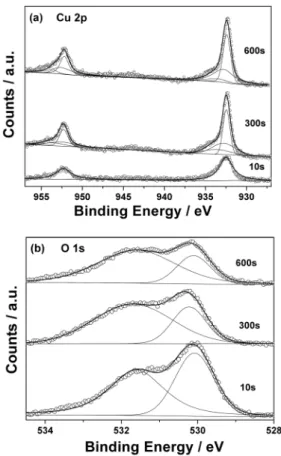
Size-Controlled Cu 2 O Nanocubes by Pulse Electrodeposition

You-Jung Song, Sang-Beom Han, Hyun-Hwi Lee

, and Kyung-Won Park*

Department of Chemical and Environmental Engineering, Soongsil University, Seoul 156-743, Republic of Korea

Pohang Accelerator Laboratory, San-31 Hyoja-dong, Pohang, Kyungbuk, 790-784, Republic of Korea

(Received January 20, 2010 : Accepted February 8, 2010)

Abstract : In this work, highly uniform size-controlled Cu

2

O nanocubes can be successfully formed by means of pulse electrodeposition. The size distribution, crystal structure, and chemical state of deposited Cu

2

O nanocubes are characterized using scanning electron microscopy, trans- mission electron microscopy, X-ray diffraction and X-ray photoelectron spectroscopy. The phase transition from Cu

2

O to Cu can be controlled by constant current electrodeposition as a function of deposition time. In particular, the size of the Cu

2

O nanocubes can be controlled using pulse electrodeposition as a function of applied current density.

Keywords : Cu

2

O Nanocube, Size control, Pulse electrodeposition, Phase transition

1. Introduction

Cuprous oxide (Cu

2

O) crystal structure has advan- tages of no toxicity, low cost, availability, and high absorption coefficient at 2.17 eV (438 nm).

1,2)

Such dis- tinct properties make Cu

2

O potential candidates for solar energy cell, catalysis, and gas sensors.

3-5)

In addition, the Cu

2

O phase is useful for negative electrodes in lithium ion batteries and for photochemical decomposition of water into O

2

and H

2

under visible light irradiation.

6-8)

It has been well known that the shape and size-control- ling of inorganic materials has great effects on their widely varying properties.

9)

Many efforts have been inten- sively devoted to the synthesis of Cu

2

O with a variety of shapes using electrochemical, thermal oxidation, solution- phase synthesis, sputtering, and chemical vapour depo- sition.

10-17)

Among them, pulse electrodeposition method was found to be useful for nanostructure fabrication because of simple operation and uniform deposition.

18-20)

However, since it is stable in an extremely narrow range, the Cu

2

O phase should be carefully fabricated.

Here, we report phase transition between Cu

2

O and Cu and size-controlling of Cu

2

O nanocubes using electrodeposition method. Using scanning electron microscopy (SEM), transmission electron microscopy (TEM), X-ray diffraction (XRD) and X-ray photo-

electron spectroscopy (XPS), size distribution, crystal structure, and chemical state of the electrodes were characterized.

2. Experimental

The Cu

2

O and Cu on indium tin oxide (ITO) glass were electrodeposited in 5 mM copper sulfate (CuSO

4

) aqueous solution. Electrodeposition was carried out under a constant mode or pulse mode, using a three-electrode cell with a Pt wire, an Ag/AgCl electrode and ITO glass as a counter, reference and working electrode, respec- tively. In case of an electrodeposition by constant current mode, −1 mA/cm

2

of direct current was applied for 10, 60, 300 and 600 s, respectively. In addition, Cu

2

O nanocubes were prepared by pulse electrodeposition from

−1 to −4 mA/cm

2

of pulse current with the 0.1 s on-time and 0.3 s off-time for 10 s at room temperature.

The morphology of deposited films was observed by means of SEM (JEOL JSM-6360A). The SEM inves- tigation was carried out at room temperature at a volt- age of 13 kV. TEM investigation was carried out using a Phillips-F20 Electron Microscope at an accelerating voltage of 200 kV and Cu grid was used as substrates.

The crystal structures of the films were confirmed by XRD (Pohang Accelerator Laboratory, 5A HFMS). In order to analyze and compare the surface chemical states of the samples, XPS was carried out using a VG Scientific (ESCALAB250, Korea Basic Science

*E-mail: [email protected]

(2)

Institute, Busan Branch) photoelectron spectrometer.

The X-ray source was Al K

a

with 1486.6 eV operating at 150 kV and 150 W. The base pressure of the system was 2 × 10

−9

Torr.

3. Results and discussion

Fig. 1 shows SEM images of electrodes electrodep- osited at −1 mA/cm

2

for 10, 60, 300, and 600 s. At the deposition time of 10 s, as shown in Fig. 1(a), the shape of the electrode is found to be cube. However, as shown in Fig. 1(b) and (c), as the deposition time in- creases, the density of cube in the electrodes is dimin- ished and starts to agglomerate. Thus, as shown in Fig. 1(d), at the deposition time of 600 s, the cube in the electrode completely disappears with complete agglomeration. To identify crystal structures in the electrodes, as shown in Fig. 1(e), the XRD analysis

was carried out. At the deposition time of 10 s, as indicated in Fig. 1(e)-a, the XRD peaks at 36.4 and 42.2 are assigned to (111) and (200) planes of Cu

2

O, respectively. Accordingly, the phase electrodep- osited at −1 mA/cm

2

for 10 s is found to be Cu

2

O cube.

However, as shown in Fig. 1(e)-b and c, as the deposition time increases from 60, 300, to 600 s, in addition to the XRD pattern of Cu

2

O, the diffraction peaks related to (111), (200) and (220) planes of Cu metal appear at 43.3, 50.4 and 74.1, respectively. This means that the peak intensity of Cu

2

O is still stronger and the XRD peaks of Cu metallic phase start to appear.

As already observed in the Fig. 1(b) and (c), the cube in the electrodes started to disappear and simultane- ously agglomerate. Therefore, the agglomerates in the electrodes must be the most of Cu metallic phase including a slight amount of Cu

2

O. In the XRD pattern of the electrode deposited for 600 s with complete agglomeration of the phase, as shown in Fig. 1(e)-d, the peak of Cu

2

O still appears. However, that of Cu metallic phase becomes relatively stronger.

To confirm chemical transition between Cu

+

and Cu

o

of the Cu

2

O and Cu, respectively, X-ray photoelectron spectra of the electrodes were obtained as shown in Fig. 2. The peak at 932.50 eV, which was corrected with reference to C1s (284.6 eV), corresponding to the binding energy of Cu2p, is in good agreement with data observed in Cu

2

O.

21)

In addition, the peak at 932.70 eV and 933.60 eV corresponds to Cu and O

2−

-adsorbed Cu, respectively.

22)

In the spectrum of the electrode deposited for 10 s, there is only Cu

2

O peak. However, as the deposition time increases from 10 to 600 s, the portion of Cu

2

O is reduced while that of Cu is increased.

The O1s core-level spectrum, peak at the lower energy of 530.3 eV, is in good agreement with O

2−

in Cu

2

O.

The XPS peak at the higher energy of 531.7 eV, is attributed to O adsorbed on the surface. It can be seen that the portion of O

2−

in Cu

2

O reduces with increasing deposition time. This demonstrates that Cu

2

O is continuously reduced to Cu metal. Thus, it is obvious that combining the XRD and XPS data, the electrodes deposited for 10 to 600 s shows phase transition between Cu

2

O and Cu.

During electrodeposition process under any given condition, cupper ions are continuously reduced. In other words, Cu

2

O is formed and then perfectly reduced to Cu metallic phase as the following equations:

Cu

2+

+ e → Cu

+

(1)

Fig. 1. SEM images of the electrodes electrodeposited for

(a) 10, (b) 60, (c) 300 and (d) 600 s. (e) X-ray diffraction

patterns of the electrodes electrodeposited for a.10, b.60,

c.300 and d.600 s. The (*), (#) and (o) mark in the Fig. 1(e)

represent XRD patterns of ITO glass, Cu

2

O and Cu,

respectively.

(3)

2Cu

+

→ Cu

0

+ Cu

2+

(2)

Cu

+

+ e → Cu

0

(3)

Fig. 3 shows SEM images of the electrodes fabricated by pulse electrodeposition with current densities of −1, −2, −3, and −4 mA/cm

2

. In the present study, on-time and total deposition time is 0.1 s and 10 s, respectively. As shown in the Fig. 3, the electrodes formed by pulse current mode consist of more than 70% of cubes and the rest of other shapes.

18-20)

However, in our study, as applied current density is increased, an average size of cubes is reduced, that is, 375, 335, 195, and 163 nm at −1, −2, −3, and −4 mA/cm

2

, respectively. Moreover, the electrode prepared by pulse electrodeposition at −1, −2, −3, and −4 mA/cm

2

displays size deviation of ±30.82, 59.91, 18.82, and 12.94, respectively. Especially, the Cu

2

O cube formed at the largest current density of −4 mA/cm

2

has the smallest size and narrowest deviation of size. Fig. 3(e) and (f) show low and high resolution TEM images of

the cube in the electrode electrodeposited at −3 mA/cm

2

. As indicated in the Fig. 3(e), the size of the cube is about 190 nm, which is well consistent with SEM image in the electrode (Fig. 3(c)). However, the single-crystal texture for the (100) orientation of Cu

2

O with d-spacing of 0.213 nm, not Cu metallic phase. Also, it is evident that the inset of the Fig. 3(e) displays transmission electron diffraction (TED) pattern indicative of (100) orientation of Cu

2

O. As a result, size-controlled Cu

2

O nanocubes could be synthesized by pulse electrodep- osition as a function of applied current density. However, although the average size of the nanocubes is de- creased, the number of the nanocubes is increased with increasing reduction current. There would be two mechanisms for the formation of the Cu

2

O nanocubes, i.e. the nucleation followed by the formation of new Cu

2

O grains and growth of existing nuclei. The depo- sition of Cu

2

O takes place only when the potential of the cathode is lower than the equilibrium electrode po- tential of the Cu

2

O/Cu

2+

; hence, a certain magnitude of cathode potential is necessary. The relationship between the overpotential and nucleation rates has been given as follows:

(4)

In the equation (4), the N is the nucleation rate; η

k

is the cathode overpotential; a and b are constants.

23)

It can be seen that higher overpotential, which is higher reduction current, produces much higher nucleation rates and larger nucleation sites in the electro-crystal- lization process. Hence, this could lead to large number of deposited Cu

2

O nanocubes with small size. As shown in Fig. 3(f), the XRD peaks at around 36.4 and 42.2 assigned to (111) and (200) plane of the Cu

2

O crystal structure, respectively, were found. The relative intensity ratios of the (200) to (111) in the Cu

2

O nano- cubes are relatively higher than that of the reference.

According to Gibbs-Wulff’s theorem, for the cubic crystallographic system, both the {111} and {100}

faces can be easily maintained in the final appearance due to an equilibrium shape in order to minimize its interfacial free energy.

24)

In addition, the morphology of the deposits shows a strong dependence on the reaction conditions, such as pH of the initial solution, temperature, reaction time and applied current density. Especially, it is likely that since the relative intensity ratios of the (200) to (111) in the Cu

2

O nanocubes are relatively higher than that of the reference, the Cu

2

O nano-cubes show

N a b

η

k2

---

⎝ – ⎠

⎛ ⎞

exp

=

Fig. 2. XPS spectra of (a) Cu2p and (b) O1s in the electrodes.

The 10, 300 and 600 s represent electrodeposition time.

(4)

Fig. 3. SEM images and size histograms of the electrodes electrodeposited at (a) − 1, (b) 2, (c) 3 and (d) 4 mA/cm

2

. (e)

Low and high magnification TEM images of Cu

2

O nanocube electrodeposited at − 3 mA/cm

2

. (The inset is TED pattern.)

(f) XRD patterns of the electrodes electrodeposited at − 1 (A), 2 (B), 3 (C) and − 4 (D) mA/cm

2

. The (*) mark represents

the XRD patterns of ITO glass.

(5)

growth along the <100> direction in the condition, which is well consistent with TEM images.

4. Conclusions

We found that phase transition between oxidative and metallic state of Cu

2

O and Cu could be controlled as a function of an electrodeposition time under reduction current mode. Especially, the Cu

2

O nanocubes without any metal- lic agglomerate were obtained by means of electrodeposi- tion during a short deposition time. Thus, the highly uniform size-controlled Cu

2

O nanocubes were fabricated using pulse electrodeposition method as a function of applied current density.

Acknowledgment

This work was supported by the National Research Foundation of Korea Grant funded by the Korean Government (NRF-2009-0065330), Human Resource Training Project for Strategic Technology, Manpower Development Program for Energy & Resources sup- ported by the Ministry of Knowledge and Economy.

References

1. G. P. Pollack and D. Trivich, ‘Photoelectric properties of cuprous oxide’ J. Appl. Phys., 46, 163 (1975).

2. R. Liu, E.A. Kulp, F. Oba, E.W. Bohannan, F. Ernst, and J.A.

Switzer, ‘Epitaxial Electrodeposition of High-Aspect-Ratio Cu

2

O (110) Nanostructures on InP(111)’ Chem. Mater., 17, 725 (2005).

3. A. O. Musa, T. Akomolafe, and M. J. Carter, ‘Production of cuprous oxide, a solar cell material, by thermal oxida- tion and a study of its physical and electrical properties’

Sol. Energ. Mat. Sol. C., 51, 305 (1998).

4. H. Xu, W. Wang, and W. Zhu, ‘Shape Evolution and Size- Controllable Synthesis of Cu2O Octahedra and Their Mor- phology-Dependent Photocatalytic Properties’ J. Phys.

Chem. B, 110, 13829 (2006).

5. S. T. Shishiyanu, T. S. Shisiyanu, and O. I. Lupan, ‘Novel NO

2

gas sensor based on cuprous oxide thin films’ Sensors Actuators B, 113, 468 (2006).

6. P. Poizot, S. Laruelle, S. Grugeon, L. Dupont, and J. M.

Tarascon, ‘Nano-sized transition-metal oxides as negative- electrode materials forlithium-ion batteries’ Nature, 407, 496 (2000).

7. C. Q. Zhang, J.P. Tu, X. H. Huang, Y. F. Yuan, X. T. Chen, and F. Mao, ‘Preparation and electrochemical performances of cubic shape Cu

2

O as anode material for lithium ion batteries’ J. Alloy Comd., 441, 52 (2007).

8. P. E. de Jongh, D. Vanmaekelbergh, and J. J. Kelly,

‘Photoelectrochemistry of Electrodeposited Cu

2

O’ J.

Electro1hem. Soc., 147, 486 (2000).

9. A. P. Alivisatos, ‘Semiconductor Clusters, Nanocrystals, and Quantum Dots’ Science, 271, 933 (1996).

10. M. J. Siegfried and K.-S. Choi, ‘Directing the Architecture of Cuprous Oxide Crystals during Electrochemical Growth’

Angew. Chem. Int. Ed., 44, 3218 (2005).

11. A. L. Daltina, A. Addadb, and J. P. Choparta, ‘Potentiostatic deposition and characterization of cuprous oxide films and nanowires’ J. Cryst. Growth, 282, 414 (2005).

12. B. Balamurugan and B. R. Mehta, ‘Optical and structural properties of nanocrystalline copper oxide thin films prepared by activated reactive evaporation’ Thin Solid Films, 396, 90 (2001).

13. L. Gou and C. J. Murphy, ‘Solution-Phase Synthesis of Cu2O Nanocubes’ Nano Lett., 3, 231 (2003).

14. Z. Wu, M. Shao, W. Zhang, and Y. Ni, ‘Large-scale synthesis of uniform Cu2O stellar crystals via microwave- assisted route’ J. Cryst. Growth, 260, 490 (2004).

15. Z. Z. Chen, E. W. Shi, Y.Q. Zheng, W. J. Li, B. Xiao, and J. Y. Zhuang, ‘Growth of hex-pod-like Cu

2

O whisker under hydrothermal conditions’ J. Cryst. Growth, 249, 294 (2003).

16. P. Taneja, R. Banerjee, and P. Ayyub, ‘Structure and properties of nanocrystalline Ag and Cu

2

O synthesized by high pressure sputtering’ Scr. Mater., 44, 1915 (2001).

17. P. R. Markworth, X. Liu, J.Y. Dai, W. Fan, T.J. Marks, and P. P. H. Chang, ‘Coherent island formation of Cu

2

O, films grown by chemical vapor deposition on MgO(110)’

J. Mater. Res., 16, 2408 (2001).

18. M. C. Tsai, T. K. Yeh, and C. H. Tsai, ‘An improved electrodeposition technique for preparing platinum and platinum-ruthenium nanoparticles on carbon nanotubes directly grown on carbon cloth for methanol oxidation’

Electrochem. Commun., 8, 1445 (2006).

19. X. Chen, N. Li, K. Eckhard, L. Stoica, W. Xia, J. Assmann, M. Muhler, and W. Schuhmann, Pulsed electrodeposition of Pt nanoclusters on carbon nanotubes modified carbon materials using diffusion restricting viscous electrolytes’

Electrochem. Commun., 9, 1348 (2007).

20. M. Sun, G. Zangari, M. Shamsuzzoha, and R.M. Metzger,

‘Electrodeposition of highly uniform magnetic nanoparticle arrays in ordered alumite’ Appl. Phys. Lett., 78, 2964 (2001).

21. C. D. Wagner, W. M. Riggs, L. E. Davis, J. E. Moulder, and G. E. Muilenber, Handbook of X-ray Photoelectron Spectroscopy, Perkin Elmer Corporation Physical Elect- ronics Division, USA, 1979.

22. A. O. Musa, T. Akomolafe, and M. J. Carter, ‘Production of cuprous oxide, a solar cell material, by thermal oxidation and a study of its physical and electrical properties’ Sol.

Energy Mater. Sol. Cells, 51, 305 (1998).

23. T. Gao, G. Meng, Y. Wang, S. Sun, and L. Zhang, ‘Electro- chemical synthesis of copper nanowires’ J. Phys. Condens.

Matter., 14, 355 (2002).

24. J. Xu and D. Xue, ‘Five branching growth patterns in the

cubic crystal system: A direct observation of cuprous

oxide microcrystals’ Acta Mater., 55, 2397 (2007).

수치

Fig. 1 shows SEM images of electrodes electrodep- electrodep-osited at  −1 mA/cm 2  for 10, 60, 300, and 600 s
Fig. 3 shows SEM images of the electrodes fabricated by pulse electrodeposition with current densities of  −1, −2, −3, and −4 mA/cm 2
Fig. 3. SEM images and size histograms of the electrodes electrodeposited at (a)  − 1, (b)  − 2, (c)  − 3 and (d)  − 4 mA/cm 2

참조

관련 문서

Detailed the microstructures of the Mo-Cu-N coatings were studied by X-ray diffraction, scanning electron microscopy and field emission transmission electron micro- scope..

The crystal structure and the surface morphology of the films were investigated using X-ray diffraction (XRD), atomic force microscopy (AFM), and scanning electron microscopy

Scanning electron microscopy and energy dispersive X-ray spectroscopy (SEM- EDS) and transmission electron microscopy and selected area electron diffraction (TEM- SAED)

The structural and morphological properties of these thick films were investigated using X-ray diffraction and scanning electron microscopy.. The structural properties of SnO 2

The physicochemical properties of the prepared Co-AC/TiO 2 composites were characterized by N 2 adsorption at 77 K, X-ray diffraction (XRD), scanning electron microscopy

The crystal structures, surface and optical properties of the phosphors are investigated using X-Ray Diffraction(XRD), Scanning Electron Microscope(SEM) and

The cordierite powders were characterized by X-ray diffraction (XRD, Rigaku), scanning electron microscope (SEM, JEOL: JSM-5610), energy dispersive spectroscopy (EDS, JEOL:

The prepared samples were characterized by X-ray diffraction (XRD), scanning electron microscopy (SEM), and the pH value was measured by pH-Meter.. 그러나 Co의 가격 상승으