New Physics: Sae Mulli,
Vol. 66, No. 4, April 2016, pp. 388∼391 http://dx.doi.org/10.3938/NPSM.66.388
Influence of the Deposition Parameters on the Microstructure and the Electrical Properties of LaNiO
3Thin Films
Tai Nguyen · Heon-Jung Kim
∗Department of Physics, College of Natural Science, Daegu University, Gyeongsan 42400, Korea (Received 14 December 2015 : revised 25 January 2016 : accepted 26 January 2016)
In this study, LaNiO3 (LNO) thin films are grown on SrTiO3 (STO) via pulsed laser deposition (PLD), and the influence of varying the laser energy density and the oxygen partial pressure on the microstructures and electrical properties is investigated. The LNO films are fabricated at a substrate temperature of 750◦C, and the energy densities and oxygen partial pressures are varied from 1.0 to 2.0 J/cm2 and from 0.1 to 0.5 Torr, respectively. The crystallinity, surface morphology, and electrical properties of the LNO films are characterized by using high-resolution X-ray diffraction (HRXRD), atomic force microscopy (AFM), and electrical resistivity measurements. The LNO films are shown to be c-axis oriented and to have root-mean-squared surface roughnesses of 0.881, 0.743, and 0.603 nm for energy densities of 1.0, 1.5, and 2.0 J/cm2, respectively. The transport measurement indicates that LNO is a good metallic-oxide material.
PACS numbers: 68.37.-d, 68.35.Ct, 68.55.Jk, 73.25.+I, 73.50.-h Keywords: LaNiO3 thin films, Conductive films, Pulsed laser deposition
I. INTRODUCTION
Among RNiO3 (R = rare earth ion) perovskites, LaNiO3(LNO) is the only member, which is a paramag- netic metal down to 0.4 K [1,2]. The bulk LNO is well ap- proximated by a pseudo-cubic perovskite structure with a = 3.83 Å [1] and thus, the oxygen octahedron is in ideal form, splitting Ni d bands into triply degenerate t2g(xy, xz, yz) and doubly degenerate eg(x2−y2, 3z2−r2) bands. As the nominal ionic configuration of Ni in LNO is Ni3+ with d7 configuration the t2g band is fully oc- cupied and the eg is singly occupied. While in bulk LNO two eg orbitals are equally occupied, the x2− y2 orbital can be more occupied due to tensile strain and two-dimensional confinement in the heterostructures [3–
6].
Up to now, significant efforts have been devoted to achieving a large orbital polarization in LNO-based het- erostructures to make an isolated and half-filled (x2–y2) band lower in energy to mimic the electronic structure
∗E-mail: [email protected]
of the cuprate high-Tc superconductors [3,4]. The pre- vious proposals based on quantum confinement and/or strain engineering was partially successful in inducing only small orbital polarization. The largest value is less than 20% [5]. Recently, A. S. Disa and coworkers [6]
demonstrated that about 50% change in the occupa- tion of Ni d orbitals was achieved by combining charge transfer between layers and inversion symmetry breaking in tricolor heterostructures. In fact, their tricolor het- erostructures were not fully optimized for orbital polar- ization and their theoretical calculations suggested that selecting a suitable insulating barrier in the [(LaTiO3)1- (LaNiO3)1-(insulator)] heterostructure could further in- crease its value.
In this study, we performed experiments to find out optimal PLD growth conditions for LNO thin films by altering the energy density and oxygen partial pressure.
The energy density and the oxygen partial pressure were changed from 1.0 to 2.0 J/cm2, and 0.1 to 0.5 Torr, re- spectively.
This is an Open Access article distributed under the terms of the Creative Commons Attribution Non-Commercial License (http://creativecommons.org/licenses/by-nc/3.0) which permits unrestricted non-commercial use, distribution, and reproduction in any medium, provided the original work is properly cited.
Influence of the Deposition Parameters on the Microstructure and the Electrical· · · – Tai Nguyen · Heon-Jung Kim 389
II. EXPERIMENTAL
In general, LNO powders could be synthesized via ei- ther the solid state reactions or sol-gel techniques. This solid reaction method, however, is known to be diffi- cult to oxidize nickel to Ni3+ at low oxygen pressures (P(O2) ≤ 1 bar) and at the high temperatures (800 – 1000◦C). In contrast, the sol-gel method easily stabilizes Ni3+ producing stoichiometric LNO at atmosphere air and at relatively lower temperatures by adding some cat- alytic chemicals. Due to this reason, we prepared LNO powders via a sol-gel route. Lanthanum nitrate hexahy- drate [La(NO3)3·6H2O] and nickel nitrate hexahydrate [ Ni(NO3)2·6H2O ] (> 99%; both from Alfa Aesar) were dissolved in 2-methoxyethanol (MOE). The concentra- tion of the precursor was adjusted to 0.25 M by adding acetic acid and ethylene glycol. After stirring at 600 rpm for 5 hours, a stable green solution was obtained. This solution was dried at 300◦C. The obtained powders were further fired at 600 ◦C and then pressed into a target.
Finally, the target was sintered at 850 ◦C in the air for 12 hours.
The LNO films were fabricated on (001) STO sub- strates (Shinkosha) via PLD technique. Lambda Physik 300 excimer laser system operating with KrF at 248 nm is used. Firstly, to investigate the influence of energy density (F), some LNO films were grown at oxygen par- tial pressure of 0.1 Torr and at the substrate temperature of 750 ◦C with the energy densities of 1.0, 1.5, and 2.0 J/cm2. Then, the influence of the oxygen partial pres- sure was investigated by depositing LNO films at 750◦C substrate temperature with 1.0 J/cm2 while the oxygen partial pressures (pO2) were varied from 0.1 to 0.5 Torr with interval of 0.1 Torr.
X-ray diffraction measurements were performed to confirm phase purity and crystallinity of LNO films with a high-resolution diffractometer using Cu K� radiation.
The surface morphology of LNO films was also investi- gated by atomic force microscopy (AFM). The temper- ature dependence of the resistivity was measured by the standard Van Der Pauw method in a temperature range from 300 down to 77 K.
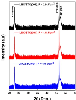
Fig. 1. (Color online) The X-ray diffraction results for a series of LNO films grown at the energy density F of 1.0, 1.5, and 2.0 J/cm2.
III. RESULT AND DISCUSSION
1. The influence of the energy density
The X-ray diffraction patterns of LNO films grown with different energy density are shown on Fig. 1. The θ–2θ scan of the films shows only the (001) and (002) peaks of the substrate and the films for all three sam- ples. The out–of–plane lattice parameter of LNO films on STO is estimated to be about 3.848 Å. No impure phase is observed. The presence of only (001) and (002) peaks indicates c-axis orientation of the films.
The AFM measurement was performed to investigate the surface morphology of these LNO films, as displayed on Fig. 2. These images revealed that three films show a smooth and homogeneous surface. The root-mean- squared surface roughness and the average grain size are 0.881 nm and 0.08 µm for 1.0 J/cm2, 0.743 nm and 0.075 µm for 1.5 J/cm2, and 0.603 nm and 0.05 µm for 2.0 J/cm2.
In order to study the electrical transport properties of these thin films, measurement of the temperature depen- dence of resistivity was performed. The results indicated
390 New Physics: Sae Mulli, Vol. 66, No. 4, April 2016
Fig. 2. (Color online) AFM images of LNO films grown on STO (001) substrate with different energy density F: F = (a) 1.0, (b) 1.5, and (c) 2.0 J/cm2.
Fig. 3. (Color online) Normalized resistance R(T)/R(300 K) of LNO films grown on STO (001) (a) at different energy densities and (b) at different oxygen partial pressures pO2: pO2 = 0.1 (black solid square), 0.2 (red solid circle), 0.3 (green solid up triangle), 0.4 (blue solid down triangle), and 0.5 Torr (cyan solid diamond).
that all three LNO films are metallic down to 77 K. Re- sistances at 300 K of three LNO films decrease with the increase of the energy density probably due to the in- crease of film thickness. As the film thickness was un- known, normalized resistance R(T)/R(300 K) were plot- ted for three samples in Fig. 3(a). Here the residual resistance ratio defined as R(300 K)/R(77 K) (RRR77) was extracted to be 1.470, 1.449, and 1.612 for the films grown at 1.0, 1.5, and 2.0 J/cm2, respectively.
2. The influence of oxygen partial pressure
For the films grown at different oxygen partial pres- sure, the measurement of electrical resistivity versus tem- perature was conducted in order to study the influence of oxygen partial pressures on the electrical transport properties of these films. Clearly, these LNO thin films
exhibit metallic behaviors. The normalized resistances R(T)/R(300 K) were plotted as before in Fig. 3(b). The RRR77 value was observed to increase as the oxygen par- tial pressure increases from 0.2 to 0.5 Torr. However, the sample grown at 0.1 Torr does not follow this trend. The RRR77 values are 1.400, 1.795, 1.931, and 2.253 for the films grown at 0.2, 0.3, 0.4, and 0.5 Torr, respectively.
On the other hand, the RRR77 values of the films grown at 0.1 Torr is 1.884. Ivan Marozau and coworkers [7]
have been demonstrated that the electronic and mag- netic properties of LaMnO3 thin films were modified by cationic ratio (La/Mn). Based on their study, it is spec- ulated that the RRR77 value of the film grown at 0.1 Torr deviates from the overall trend of the other samples because of different cationic ratio. This point should be clarified separately.
Influence of the Deposition Parameters on the Microstructure and the Electrical· · · – Tai Nguyen · Heon-Jung Kim 391
IV. CONCLUSIONS
In summary, the LaNiO3films were deposited on (001) SrTiO3 by pulsed laser deposition technique. The influ- ence of energy density and oxygen pressure on the mi- crostructure and electrical properties of LaNiO3 films were investigated. The obtained LaNiO3 films were shown to be c-axis oriented with smooth and homoge- neous surface. The transport measurements for these films displayed a metallic behavior over the temperatures region between 300 K and 77 K.
REFERENCES
[1] A. Wold, B. Post and E. Banks, J. Am. Chem. Soc.
79, 4911 (1957).
[2] P. Ganguly, N. Y. Vasantacharya, C. N. R. Rao and P. P. Edwards, J. Solid State Chem. 54, 400 (1984).
[3] J. Chaloupka and G. Khaliullin, Phys. Rev. Lett.
100, 016404 (2008).
[4] P. Hansmann, X. Yang, A. Toschi, G. Khaliullin and O. K. Andersen et al., Phys. Rev. Lett. 103, 016401 (2009).
[5] M. Wu, E. Benckiser, M. W. Haverkort, A. Frano and Y. Lu et al., Phys. Rev. B 88, 125124 (2013).
[6] A. S. Disa, D. P. Kumah, A. Malashevich, H. Chen and D. A. Arena et al., Phys. Rev. Lett. 114, 026801 (2015).
[7] I. Marozau, P. T. Das, M. Döbeli, J. G. Storey and M. A. Uribe-Laverde et al., Phys. Rev. B 89, 174422 (2014).