Epitaxial thin films of multiferroic
on conducting indium tin oxide (001) buffered
yttrium-stabilized zirconia (001) by pulsed laser deposition
M. Trassin, N. Viart, G. Versini, J.-L. Loison, J.-P. Vola, G. Schmerber, O. Crégut, S. Barre, and G. PourroyJ. H. Lee, W. Jo, and C. Mény
Citation: Appl. Phys. Lett. 91, 202504 (2007); doi: 10.1063/1.2813020 View online: http://dx.doi.org/10.1063/1.2813020
View Table of Contents: http://aip.scitation.org/toc/apl/91/20 Published by the American Institute of Physics
Epitaxial thin films of multiferroic GaFeO
3on conducting indium tin
oxide
„001… buffered yttrium-stabilized zirconia „001… by pulsed
laser deposition
M. Trassin, N. Viart,a兲 G. Versini, J.-L. Loison, J.-P. Vola, G. Schmerber, O. Crégut, S. Barre, and G. Pourroy
Institute of Physics and Chemistry of Materials of Strasbourg, UMR 7504 ULP-CNRS, 23 rue du Loess, B.P. 43, 67034 Strasbourg Cedex 2, France
J. H. Lee, W. Jo, and C. Ményb兲
Department of Physics and Division of Nanosciences, Ewha Womans University, Seoul 120 750, Republic of Korea
共Received 26 June 2007; accepted 25 October 2007; published online 14 November 2007兲 Epitaxial films of an alternative multiferroic material, GaFeO3共GFO兲, were grown by pulsed laser
deposition on yttrium-stabilized zirconia共001兲 and on conducting buffer layers of indium tin oxide 共001兲. They present a perfect epitaxial growth along the GFO 关010兴 axis and six crystallographic variants in the film’s plane. Their magnetic properties are close to those of the bulk with an out-of-plane 关010兴 hard direction and a Curie temperature of ⬃200 K. The films did exhibit ferroelectric properties when characterized by electrostatic force microscopy. © 2007 American
Institute of Physics. 关DOI:10.1063/1.2813020兴
Multiferroic materials receive a considerable renewal of interest because of the increased possibilities their properties offer to electronic devices.1–3 Recently, the multifunctional character of multiferroics has been exploited to design mag-netic tunnel junctions.4 Such junctions, presenting both magneto- and electroresistance effects, define a four-resistance-state system and constitute a major progress in spintronics. However, few materials simultaneously present magnetic and electric orderings.5 Among these materials, those presenting ferri—or ferromagnetic properties are ex-tremely rare, the vast majority being antiferromagnets.6 BiMnO3共BMO兲, which is one of the very few ferromagnetic multiferroic materials, has been until now the favorite candi-date for the fabrication of tunnel junctions.7 However, its Curie temperature of 105 K is far from room temperature and the stabilization of a pure BMO phase is rather difficult. There is a need for alternative materials. GaFeO3共GFO兲 is a
very promising one. It is ferroelectric and ferrimagnetic.8Its Curie temperature is of about 200 K and may be increased to values above room temperature by increasing the Fe content
x of the Ga2−xFexO3 cell 共TCurie= 350 K for x = 1.4兲.9 The
physical properties of GFO are well documented in the bulk form since the 1960s. It was discovered by Remeika in 1960.10 Its crystallographic structure共orthorhombic unit cell in the space group Pc21n with a = 0.875 12± 0.000 08 nm, b = 0.939 93± 0.000 03 nm, and c = 0.508 06± 0.000 02 nm兲
was described by Abrahams et al.11a few years later on the basis of a proposition made by Wood.12According to Levine
et al.,13 its magnetic ordering temperature is 240 K and the low temperature spontaneous moment is of 0.76B per Fe
atom. Another extremely interesting property of this material is the magnetoelectric effect observed by Rado14in the bulk.
However, applications of the multiferroic properties of this very promising material in electronic devices require the fabrication of thin films. Up to now, only one paper deals with this fabrication.15While the crystallographic properties of the films are the key point on which the physical proper-ties depend, no particular focus was made in that paper on the crystallographic properties of the films, especially in plane. Another crucial point that needed to be addressed is the existence of a crystallographically compatible material suitable to be used as a conducting electrode. It has indeed been predicted16 and experimentally proven for 共100兲 ori-ented CoFe/ MgO / CoFe junctions17 that fully epitaxial tun-nel barriers can give rise to higher tuntun-neling spin polariza-tion than amorphous ones because of highly spin dependent evanescent decay of certain wave functions. In this letter, we report the fully epitaxial growth of GFO on conducting in-dium tin oxide 共ITO兲 buffered yttrium-stabilized zirconia 共YSZ兲 共001兲 by pulsed laser deposition 共PLD兲 and present the crystallographic relationships between the films and the substrate. The implications of these relationships on the mag-netic properties will also be given. The ferroelectric
proper-a兲Electronic mail: [email protected]
b兲Permanent address: Institute of Physics and Chemistry of Materials of
Strasbourg, UMR 7504 ULP-CNRS, 23 rue du Loess, B.P. 43, 67034 Strasbourg Cedex 2, France.
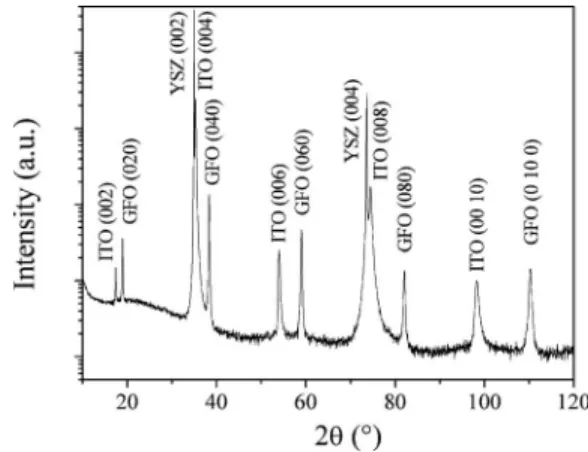
FIG. 1. XRD pattern of a GFO film grown at 900 ° C under 100 Pa O2: N2,
on an epitaxially ITO buffered YSZ共001兲 substrate.
APPLIED PHYSICS LETTERS 91, 202504共2007兲
ties of the deposited GFO films were demonstrated through polarization–electric field 共P-E兲 hysteresis loops measured by electrostatic force microscopy共EFM兲.
Films have been realized using a KrF excimer laser 共=248 nm兲 with a 10 Hz repetition rate and a fluence of 1 J / cm2. The ITO and GaFeO
3 targets were made from
sin-tering the relevant powders at 1400 ° C for 24 h 关In2O3
doped with 10 wt. % SnO2共Aldrich兲 for ITO and a stoichio-metric mixture of high purity Ga2O3 共99.99%, Fluka A.G.兲
and Fe2O3共99%, Prolabo兲 for GaFeO3兴. A 60 nm thick ITO
conducting layer was first deposited under 7⫻10−3Pa
O2: N2 at 600 ° C on YSZ 共001兲 substrate. A 180 nm thick
GaFeO3 layer was then deposited under a wide range of deposition substrate temperatures 共600–900 °C兲 and reac-tive gas partial pressures共50–100 and 20–100 Pa for O2and
O2: N2, respectively兲. After the deposition, the samples were
cooled down to room temperature under the gas deposition pressure. The sample crystallographic structure was charac-terized by x-ray diffraction.-2scans were collected with a D500 Siemens diffractometer equipped with cobalt radiation 共K␣= 0.178 901 nm兲. scans and reciprocal lattice map-pings were made using a D8 Siemens diffractometer equipped with copper radiation 共K␣= 0.154 059 nm兲. The magnetic properties were studied using a superconducting quantum interference device magnetometer 共Quantum De-sign兲. The ferroelectric characterization of the samples was performed at room temperature with a commercial atomic force microscope 共Nanofocus, Inc.兲, modified to a dynamic contact mode EFM, operating with a lock-in modulation fre-quency of 19 kHz and controlled through the WSXM
software.18Details on the experimental setup and ideas of the
dynamic contact mode were published earlier.19,20In our ex-periments, the cantilever is in heavily doped Si and has a spring constant of 0.5 N / m and a tip apex radius of 20 nm. Local polarization–electric field共P-E兲 hysteresis loop mea-surements were performed on single polarization domains with a dc voltage swept between +10 and −10 V.21
The optimal deposition conditions for GaFeO3,
deter-mined from direct deposition on YSZ substrates, appear to be at 900 ° C under a 100 Pa partial pressure for both reactive gases O2 and O2: N2. For lower reactive gas pressures and
temperatures, we observed a parasitic phase corresponding to the cubic magnetite phase. The x-ray diffraction pattern of a GFO film deposited on an ITO buffered YSZ substrate at 900 ° C under an O2pressure of 100 Pa is shown in Fig.1. It
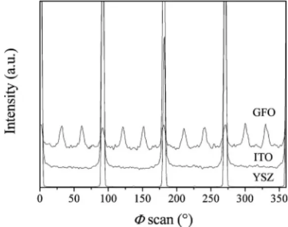
clearly demonstrates pure c- and b-axis growths of ITO and GFO, respectively.scans of the GFO兵062其, ITO 兵408其, and YSZ兵204其 planes were carried out 共Fig.2兲. They present the
awaited 90° periodicity for both cubic ITO and YSZ peaks and a 30° periodicity for the GFO one. The ITO layer is perfectly epitaxially grown on YSZ with only one variant. The GFO crystallites, on the other hand, present six variants having in-plane orientations every 30° each. The very small mismatch共1.1%兲 between the two cubic YSZ and ITO lattice parameters 共aYSZ= 0.5139 nm and aITO= 1.016 nm⬇2aYSZ兲
explains the high crystalline quality and monovariance of the ITO films on YSZ. The different orientations of the GFO crystallites can be explained considering the different matching possibilities between the GFO and ITO lattices: cGFO= 0.5086 nm and aITO= 1.016 nm⬇2cGFO
共0.2% mismatch兲, on the one hand, and
冑
aGFO2 + cGFO2 ⬇aITO共0.4% mismatch兲, on the other hand. The angle between
a and the diagonal of the ac plane of the GFO cell is ␣= cos−1共aGFO/
冑
aGFO2
+ cGFO2 兲⬇30° 关Fig. 3共a兲兴. This allows
FIG. 2.scans of the GFO兵062其, ITO 兵408其, and YSZ 兵204其 planes show-ing a 30° periodicity for multivariant GFO and 90° periodicities for both cubic monovariant ITO and YSZ.
FIG. 3.共a兲 Illustration of the consequence of the
冑
aGFO2 + c GFO 2 ⬇aITO
rela-tionship.共b兲 The six resultant in-plane possible orientations of a GFO 共0k0兲 cell共gray兲 on ITO 共001兲.
FIG. 4. Variation of the共a兲 magnetization with temperature under a 200 Oe applied field and共b兲 hysteresis loops at 5 K 共b兲 along the three YSZ sub-strate crystallographic directions共a and b are in plane and c is out of plane兲. 202504-2 Trassin et al. Appl. Phys. Lett. 91, 202504共2007兲
the existence of the six variants shown in Fig.3共b兲, located every 30°. Magnetization measurements were performed on 3⫻3 mm2 samples of GFO/ITO/YSZ films, in two
perpen-dicular in-plane and in the out-of-plane directions. The mag-netization versus temperature measurements关Fig.4共a兲兴, per-formed in a 200 Oe applied magnetic field, reveal a Curie temperature of about 200 K. The hysteresis cycles 共M-H兲 关Fig.4共b兲兴 were measured at 5 K and show a saturation mag-netization of⬃0.6B per Fe atom. Both magnetic
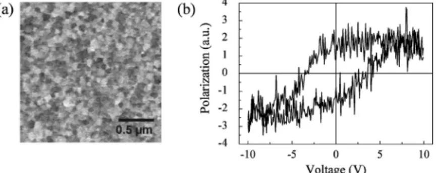
measure-ments present a strong anisotropy with a hard magnetization direction along the GFO b axis 共out of plane兲, but no in-plane anisotropy between the two chosen perpendicular di-rections. The in-plane coercive field reaches the relatively high value of about 2500 Oe at 5 K. Apart from the in-plane isotropic behavior, all the measured magnetic properties are similar to what are observed in bulk.13 The absence of in-plane anisotropy is due to the existence of six crystallo-graphic variants, separated by only 30°. Magnetic measure-ments are in complete agreement with the crystallographic characterization of the GFO layers. EFM imaging of the samples gives a rough polarization domain size of⬃0.2 m 关Fig.5共a兲兴. Figure5共b兲shows local P-E hysteresis measure-ments obtained by EFM on one particular polarization do-main sweeping E from −10 to + 10 V. Such a polarization loop is a positive evidence of the ferroelectric nature of the elaborated GFO films.
In conclusion, we have shown the possibility to obtain epitaxial thin films of the extremely promising multiferroic material GaFeO3 on perfectly crystallographically matching
ITO conducting electrodes. The magnetic properties of the GFO thin films are close to those of the bulk with a relatively high Curie temperature of ⬃200 K, a hard magnetization direction out of the plane, and a saturation magnetization of
0.6Bper Fe atom. The ferroelectric nature of the elaborated
GFO films was shown by EFM P-E loop measurements. This work was supported by the Hubert Curien Partner-ship “Star Project,” Ref. No. 16559YG.
1N. Hur, S. Park, P. A. Sharma, J. S. Ahn, S. Guha, and S. W. Cheong,
Nature共London兲 429, 392 共2004兲.
2Ch. Binek and B. Doudin, J. Phys.: Condens. Matter 17, L39共2005兲. 3S. Ju, T.-Y. Cai, G.-Y. Guo, and Z.-Y. Li, Phys. Rev. B 75, 064419共2007兲. 4M. Gajek, M. Bibes, S. Fusil, K. Bouzehouane, J. Fontcuberta, A.
Barthélémy, and A. Fert, Nat. Mater. 6, 296共2007兲.
5N. A. Hill, J. Phys. Chem. B 104, 6694共2000兲.
6G. A. Smolenskii and I. E. Chupis, Sov. Phys. Usp. 25, 475共1982兲. 7M. Gajek, M. Bibes, A. Barthélémy, K. Bouzehouane, S. Fusil, M. Varela,
J. Fontcuberta, and A. Fert, Phys. Rev. B 72, 020406共R兲 共2005兲.
8M. J. Han, T. Ozaki, and J. Yu, Phys. Rev. B 75, 060404共R兲 共2007兲. 9C. H. Nowlin and R. V. Jones, J. Appl. Phys. 34, 1262共1963兲. 10J. P. Remeika, J. Appl. Phys. 31, S263共1960兲.
11S. C. Abrahams, J. M. Reddy, and J. L. Bernstein, J. Chem. Phys. 42,
3957共1965兲.
12E. A. Wood, Acta Crystallogr. 13, 682共1960兲.
13B. F. Levine, C. H. Nowlin, and R. V. Jones, Phys. Rev. 174, 571共1968兲. 14G. T. Rado, Phys. Rev. Lett. 13, 335共1964兲.
15D. C. Kundaliya, S. B. Ogale, S. Dhar, K. F. McDonald, E. Knoesel, T.
Osedach, S. E. Lofland, S. R. Shinde, and T. Venkatesan, J. Magn. Magn. Mater. 299, 307共2006兲.
16P. Mavropoulos, N. Papanikolaou, and P. H. Dederichs, Phys. Rev. Lett.
85, 1088共2000兲.
17S. Parkin, C. Kaiser, A. Panchula, P. M. Rice, B. Hughes, M. Samant, and
S. H. Yang, Nat. Mater. 3, 862共2004兲.
18I. Horcas, R. Fernandez, J. M. Gomez-Rodriguez, J. Colchero, J.
Gomez-Herrero, and A. M. Baro, Rev. Sci. Instrum. 78, 013705共2007兲.
19J. W. Hong, S. I. Park, and Z. G. Khim, Rev. Sci. Instrum. 70, 1735
共1999兲.
20J. W. Hong, K. H. Koh, S. I. Park, S. I. Kwun, and Z. G. Khim, Phys. Rev.
B 58, 5078共1998兲.
21Y. J. Oh, J. H. Lee, and W. Jo, Ultramicroscopy 106, 779共2006兲.
FIG. 5. 共a兲 EFM surface charge image and 共b兲 local P-E hysteresis loop measured for voltage sweeping be-tween −10 and +10 V on one particular polarization domain.