45
A Differential Current-to-Time Interval Converter Using Current-Tunable Schmitt Triggers
Won-Sup Chung*★
Abstract
A differential current-to-time interval converter is presented for current mode sensors. It consists of a ramp voltage generator, a current mode sensor, a reference current source, two current-tunable Schmitt triggers, a one-shot multivibrator, and two logic gates. The design principle is to apply a ramp voltage to each input of the two current-tunable Schmitt triggers whose threshold voltages are proportional to the drain current values of the current mode sensors. A proposed circuit converts a current change in the ISFET biosensor into its equivalent pulse width change. A prototype circuit built using TSMC 0.18 nm CMOS process exhibit a conversion sensitivity amounting to 726.9 ㎲/pH over pH variation range of 2-12 and a linearity error less than
±0.05 %.
Key words : differential current-to-time interval converter, current mode sensor, ISFET biosensor, current-tunable Schmitt trigger, operational transconductance amplifier
* Dept. of Semiconductor Engineering, Cheongju University
★ Corresponding author
E-mail:[email protected], Tel:+82-43-229-8462
※ Acknowledgment
This work was supported by the research grant of Cheongju University (2016. 03. 01-2018. 02. 28)
Circuit simulation tools were supported in part by IDEC in Korea.
Manuscript received Nov, 30, 2017; revised, Dec, 6, 2017 ; accepted, Dec, 20, 2017.
This is an Open-Access article distributed under the terms of the Creative Commons Attribution Non-Commercial License
(http://creativecommons.org/licenses/by-nc/3.0) which permits unrestricted non-commercial use, distribution, and
reproduction in any medium, provided the original work is properly cited.
I. INTRODUCTION
The sensor represents the first and main element in measurement and control systems. All sensors may be of two kinds as reported in Table 1: passive and active [1]. Typical passive sensors are resistive bridge sensors. One of their signal processing circuits is reported in [2]. In order to apply the active sensors which directly produce an out current in a variety of applications dealing with chemical measurements as well as biomedical diagnoses, a precision read-out circuit connected to the sensor is indispensable. These sensor measurement circuits can be voltage or current mode of operation.
Current-mode circuits can obviously provide some advantages over voltage-mode implementations when the analog signal to be processed comes in
Main group Type of sensor
Type of signal
Typical range Active
sensors
Thermopiles, pyroelectric, piezoelectric
Voltage nV mV
pyroelectric, magnetic
Current nA mA
Passive sensors
Humidity, gas, pressure
Capacitance fF nf
Piezoelectric Charge fC pC
Pressure, chemical,
gas
Resistance k G
form of a current (e.g. the output current from a photodetector), since they can perform a straight conversion of the signal without needing current-voltage converters [3].
Table 1. Active and passive sensors and their typical electrical outputs
The current-mode method is a promising approach because of its easy current differencing operation, wide dynamic range, and lower power consumption. An analog read-out circuit by using the operational floating current conveyor (OFCC) as a current-mode device is reported in [4]. It has good linearity, but it needs the analog-to-digital (A/D) converter to acquire a digital output.
In this paper, we present a new current-to-time interval converter with good linearity. The output time interval is proportional to the differential current of current mode sensor and reference current. The converter circuit is a modified version of the circuit in [5], but its operation principle is different. The design principle of the converter is to apply a ramp voltage to each input of the two current-tunable Schmitt triggers whose threshold voltages are proportional to current values of the current mode sensors.
Ⅱ. CIRCUIT DESCRIPTION AND OPERATION
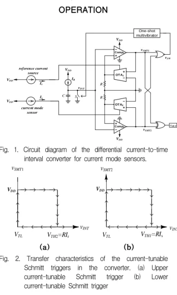
Fig. 1. Circuit diagram of the differential current-to-time interval converter for current mode sensors.
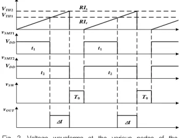
Fig. 2. Transfer characteristics of the current-tunable Schmitt triggers in the converter. (a) Upper current-tunable Schmitt trigger (b) Lower current-tunable Schmitt trigger
Fig. 1 shows the circuit diagram of the proposed differential current-to-time interval converter for current mode sensors. It consists of a current mode sensor, a reference current source, two current-tunable Schmitt triggers, a ramp voltage generator, a one-shot multivibrator, and two logic gates. The upper current-tunable Schmitt trigger is composed of a voltage comparator (Comp1), an operational transconductance amplifier (OTA1), and a resistor R. Similarly, the lower current-tunable Schmitt trigger is composed of Comp2, OTA2, and R. The transfer characteristics of the current-tunable Schmitt triggers are shown in Fig. 2. It is notable that the threshold voltages of the upper current-tunable Schmitt trigger are proportional
C S
Ir
Is
vOUT
vSMT1
vSMT2
vSW Comp1
OT A1
Comp2 OT A2
R R vINT
VDD
VDD
VDD
VDD
VDD
One-shot multivibrator
IR
reference current source
current mode sensor
(a) (b)
vSMT2
vINT
VTL VTH1=RIs
vSMT1
vINT
VTL
VDD
VDD
VTH2=RIr
to output current of the reference current source , whereas the threshold voltages of the lower current-tunable Schmitt trigger are proportional to the output current of the current mode sensor .
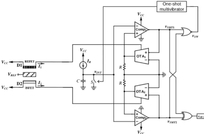
To see how the differential current-to-time interval converter operates, refer to Fig. 3, which shows the signal waveforms at the various nodes of the converter, and assume that both of the current-tunable Schmitt triggers are at their positive saturation levels
. Prior to the start of the conversion cycle, the switch S connected in the ramp voltage generator is closed, thus discharging the timing capacitor of the ramp voltage generator and setting the input voltage of the current-tunable Schmitt triggers to 0 V. The conversion cycle begins with opening the switch S. Since the reference current flows through the capacitor, rises linearly with a slope of
. When reaches the high threshold voltage of the upper Schmitt trigger , the
output of the upper Schmitt trigger falls to zero and the output of the Exclusive OR gate becomes high. Denoting the time duration for which keeps , we can
write
1 TH1 r
R R
C C
t V RI
I I
= =
(1)
Fig. 3. Voltage waveforms at the various nodes of the converter.
The conversion process continues until
reaches the high threshold voltage of the lower Schmitt trigger . At this instant the output of the lower Schmitt trigger falls to zero, thereby
becomes low and the output of the NOR gate
becomes high. The switch S in the ramp voltage generator is now closed and thus clamping the voltage to ground. This in turn triggers the Schmitt triggers, causing their outputs rise to , respectively, and
go to low. The switch S is now opened after the fixed duration of the one-shot multivibrator and a new conversion process is started. Denoting the time duration for which keeps , we can write
2 TH2 s
R R
C C
t V RI
I I
= =
(2)
The time interval of pulse is given by
2 1
t t t
D = - (3)
Combining (1) and (2) onto (3), one can obtain
VTH1
vSMT1
RIs
vINT
t1
vSW
VTH2
vSMT2
RIr
t2
t1
t2
vO UT
Δt
Δt VD D
VD D
T0 T0
( s r) ( s r)
R R
C CR
t RI RI I I
I I
D = - = -
(4)
Equation (4) indicates that the converter offers an equivalent output pulse whose time interval is proportional to the difference between the current mode sensors. It also indicates that the conversion sensitivity of converter can be controlled by the ratio of the dc current and resistor R. The digital equivalent output can be obtained by counting the time interval with an external clock.
Ⅲ. SLMULATION RESULTS
In order to test its applicability, the proposed converter is used to implement ISFET measurement circuits [6]. Fig. 4 shows the circuit diagram of the differential current-to-time interval converter for ISFET biosensor, where REFET is a passivated FET.
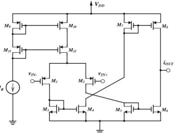
In order to the theoretical prediction of the proposed converter, we use Cadence for the simulation of the converter with TSMC 0.18 nm process. CMOS implementation of the OTAs is shown in Fig. 7. The aspect ratios (W/L) of the MOS transistors were taken as 20/1 for –
and 40/1 for –. CMOS implementation of the comparator is shown in Fig. 8. The aspect ratios of the MOS transistors were taken as 20/1 for – and 10/1 for –. The supply voltages was 3.3 V. The resistor R was 20 kΩ. The ISFET and REFET has conversion sensitivity of 7.2 ApH and 1.7 ApH for pH, respectively [7].
Fig. 4. Circuit diagram of the differential current-to-time converter for ISFET biosensor.
Fig. 5. Circuit diagram of the one-shot multivibrator.
Fig. 6. Circuit diagram of the ramp voltage generator.
The one-shot multivibrator shown in Fig. 5 was constructed by using two NOR gates, a capacitor C0 of 47 nF, and a resistor R0 of 25 kΩ. The following component values were
C S
REFET
ISFET VREF
D1
D2 I1
I2
vOUT
vSMT1
vSMT2
vSW Comp1
OTA1
Comp2 OTA2
R R vINT
VCC
VCC
VCC
VCC
VCC
One-shot multivibrator
IR
VDD
R0
C0
S vSW
C S
vIN T VDD
VDD
M1 M2
M4 M3
RB
in Fig. 6: =100 nF and = 15 ㎂. A
Wilson current mirror and a resistor of 95.5 kΩ were used for producing the DC current source
.
The simulation results are shown in Fig.
9. It appears that the conversion sensitivity amounts to 726.9 ㎲/pH over the pH variation range of 2-12. The linearity error of the conversion characteristic is less than ±0.05 %.
Fig. 7. CMOS implementation of the OTAs.
Fig. 8. CMOS implementation of the comparators.
Fig. 9. Measured time interval versus pH characteristic of the differential current-to-time converter for ISFET biosensors and its linearity error.
Ⅳ. CONCLUSION
A new circuit converting a current change into its equivalent time interval change has been described. The converter features high sensitivity and good linearity. These properties together with its low power perform make the circuit suit for implementing the ‘smart sensor' using the current mode sensors, which gives a digital output directly connectable to a microprocessor. The proposed converter is expected to find wide applications in signal processing of differential current sensors.
REFERENCES
[1] A. D. Marcellis, and G. Ferri, “Analog circuits and systems for voltage-mode and current-mode sensor interfacing,” Chap. 1, 2011.
[2] Z.-H. Shang, W.-S. Chung, and S.-H. Son,
“A resistance deviation-to-time interval converter based on dual-slope integration,”
j.inst.Korean.electr.electron.eng, vol. 19, No. 4, pp. 479-485, 2015.
DOI:10.7471/ikeee.2015.19.4.479
VDD
M1
vIN- vIN+
IB
M2
M3 M4
M7 M8
M5 M6
M9 M10
M11 M12
iOUT
M5 M6
M7 M8
vIN+ vIN-
vOUT M1 M2
M3 M4
M9 M10
IB
VDD
pH
4 2
2 8 10 12
Pulse width, T(ms)
2 4 6 8
Linearity error (%)
-0.10 -0.05 0.00 0.05 0.10
Time interval (ideal) Time interval (simulation) Linearity error
[3] L. Ravezzi, D. Stoppa, and G. F. Dalla Betta, “Current-mode A/D converter,”
ELECTRONICS LETTERS, vol. 34, No. 7, pp.
615-616, 1998.
DOI: 10.1049/el:19980422
[4] W. Y. Chung, C. H. Yang, D.G. Pijanowska, A. Krzyskow, and W. Torbicz, “ISFET interface circuit embedded with noise rejection capability,” ELECTRONICS LETTERS, vol. 40, No. 18, pp. 1115-1116, 2004.
DOI: 10.1049/el:20045388
[5] H. Kim, W.-S. Chung, H.-J. Kim, and S.-H.
Son, “A Resistance Deviation-to-Pulsewidth Converter for Resistive Sensors”, IEEE Trans.
Instrum. Meas., vol. 58, pp. 397–400, 2009.
DOI: 10.1109/TIM.2008.2003318
[6] C.-S. Won, and W.-S. Chung, “A Differential Current-to-Time Converter for ISFET Biosensors”, ITC-CSCC, pp. 217–220, 2009.
[7] Y. H. Ghallab, W. Badawy and K. V. I. S.
Kaler, “A novel pH sensor using differential ISFET current mode read-out circuit", MEMS, NANO and Smart Systems, 2003. Proceedings.
International Conference on, pp. 255-258, 2003.
DOI:10.1109/ICMENS.2003.1222002
BIOGRAPHY
Won-SupChung (Member)
Photo
1977 : BS degree in Electrical Communication Engineering, Hanyang University.
1979 : MS degree in Electrical Communication Engineering, Hanyang University
1986 : PhD degree in Electrical Science Engineering, Shizuoka University From 1986 to Present : Professor in Department of Semiconductor Engineering, Cheongju University.