반도체디스플레이기술학회지 제18권 제1호(2019년 3월) Journal of the Semiconductor & Display Technology, Vol. 18, No. 1. March 2019.
38
Direct Writing Lithography Technique for Semiconductor Fabrication Process Using Proton Beam
Kwan Do Kim
*†*†
Dept. of Convergence Software, College of IT Engineering, Pyeongtaek University
ABSTRACT
Proton beam writing is a direct writing lithography technique for semiconductor fabrication process. The advantage of this technique is that the proton beam does not scatter as they travel through the matter and therefore maintain a straight path as they penetrate into the resist. The experiment has been carried out at Accelerator Mass Spectrometry facility. The focused proton beam with the fluence of 100 nC/mm
2was exposed on the PMMA coated silicon sample to make a pattern on a photo resist. The results show the potential of proton beam writing as an effective way to produce semiconductor fabrication process.
Key Words : Proton beam writing, Lithography, Accelerator Mass Spectrometry, Semiconductor fabrication process
1
1. Introduction
X-ray lithography, EUV lithography, and electron beam lithography are widely used in the semiconductor industry.
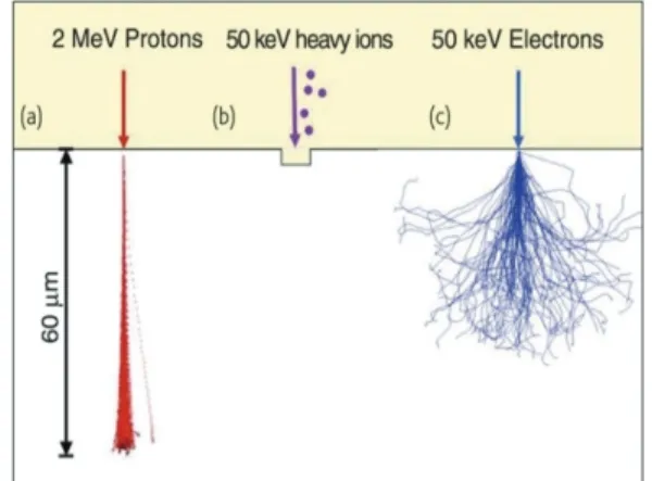
Proton beam writing is expected to be one of the next generation lithography technique to manufacture the micro and nano-sized structures. As the scattering of the proton beam which have a high energy of several MeV is very small, the technique is expected to make sub-100nm structures with a high aspect ratio. Proton beam has the following merits compared with X-ray, EUV(Extreme Ultraviolet) and electron beam. First, the formation of pattern with high resolution is possible as the scattering is so small. Second, direct writing process without expensive masks is possible compared with X-ray or EUV. Third, the depth of the proton penetrating into resist materials is controlled by the acceleration energy. Especially, based upon the first advantage, the proton beam writing is effective for micromachining with a capability to produce structures on thick resist with a high aspect ratio [1]. A comparison between p-beam writing, FIB, and e-beam writing is shown in Fig. 1 [2]. Recently several proton
†
E-mail: [email protected]
beam writing facilities have come at various laboratories around the world. Review of the progress by the research groups in the field of micro-machining using proton beam are well described [3-12]. In this paper, we examine the possibility of proton beam writing to make a pattern on silicon. The results are discussed to form a line and space pattern after exposure to a highly focused beam of MeV protons on the positive photo resist.
Fig. 1. Comparison between (a) p-beam writing, (b) FIB, and
(c) e-beam writing. This figure shows schematically
the difference between the three techniques.
Direct Writing Lithography Technique for Semiconductor Fabrication Process Using Proton Beam
Journal of KSDT Vol. 18, No. 1, 2019 39
2. Proton Beam Writing
PMMA (950PMMA A Resist, MicroChem Corp.) is used as the positive photo resists. PMMA (polymethyl methacrylate) is a versatile polymeric material that is well suited for many imaging and non-imaging microelectronic applications.
PMMA is most commonly used as a high resolution positive resist for direct write e-beam as well as X-ray and deep UV(Ultraviolet) microlithographic process. In order to prepare the samples PMMA was dropped and spin-coated at a speed of 100 rpm for 30 sec on a 4 inch p-type silicon (100) substrate. The spin-coated PMMA film was then baked at 180
O
C for 3 min. PR spin coater (LSM 250, Sawatec) was used.
The PMMA film was 5 ㎛ in thickness. Spectroscopic Ellipsometer (M-2000, J. A. Woollam) was used to extract the thickness of the photo resist. Generated and experimental results shows that although there is a little deviation within the wafer location, average 4910 nm(≈5 ㎛) was extracted. The cross section of the PR coated silicon wafer was measured and analyzed by HR FE-SEM(JEOL JSM-740F, JEOL) also.
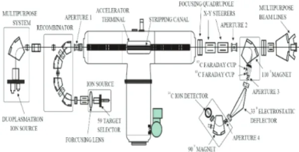
Fig. 2. Schematic layout of the Tandetron AMS/MPS system.
AMS facility (Tandetron 4130 AMS/MPS System, High Voltage Engineering Europe) is used for proton beam exposure experiment. Tandetron AMS / multipurpose beam line(MPS) has a dedicated
14C AMS beam line and an additional MPS with separate ion sources. AMS facility is mainly used to measure the scientific date in chronology using the carbon source and was utilized after replacing the carbon source gas with H
2for this experiment. The beam acceleration voltage of AMS facility is 3 MeV ~ 6 MeV, electric currents are 5x10
-13~ 2x10
-8A and it uses Ar gas as the charge stripper. The schematic drawing of the Tandetron AMS/MPS system is shown in Fig. 2. AMS facility system beam specification is shown in Table 1.
2cm x 2cm silicon sample coated with 5 ㎛ PMMA
was prepared for proton exposure. To calculate the beam currents the amount of proton was measured using Faraday cup for 12 times for each 50 sec. Simple numerical formula Q(charge)=I(currents) x T(time) is used in order to calculate the beam currents. Namely, after deciding Q(charge) using Faraday cup, dividing with time and electric currents can be obtained.
Table 1. AMS facility system beam specification
Item Spec.
Beam emittance 2~6nm*rad
Optimal beam currents 20nA
Minimal beam spot 1.0mm
Optimal beam energy 3MeV
Charge stripper Ar gas
The amount of proton was calculated according to beam currents. The average proton beam fluence was 58.75x10
-10C and the currents were calculated to 0.1175 nA. Based on the calculated beam currents, proton fluence which will be exposed are split into 4 conditions and decide the exposure time according to that. Exposure time is 852sec to set the proton beam fluence of 100nC/mm
2. Acceleration voltage of the proton beam is 3 MeV. For the line and space pattern formation 200 ㎛/68 ㎛ width and 5 mm length slit was fabricated and installed to the end of the AMS beam line where the proton beam comes out.
After proton beam exposure according the split conditions, developing process is performed in IPA-water (7:3) solution.
For the case of proton beam fluence 100 nC/mm
2, developing time is split into 4 conditions (10, 15, 20, 30 min). After developing process the sample is rinsed in deionized water and observed.
The sample preparation is the same as the first experiment. The proton beam fluence is 100 nC/mm
2. The slit size is scaled down to 68 ㎛ width and 5 mm length.
Projected range according to each ion energy was
calculated with SRIM simulation based on the PMMA
characteristics [13]. Projected range means the depth
position, in which the amount of proton decreases 1/e from
the surface and it is used as the judging the distance of
travel after beam incidence actually. According to the
calculated results, 400 keV ion energy is thought to be
suitable because the projected range is approximately 5 ㎛,
Kwan Do Kim
반도체디스플레이기술학회지 제18권 제1호, 2019 40
but the proton beam with 3 MeV ion energy was used for the stabilized conditions of the beam line.
3. Results and Discussions
Fig. 3 shows the image of the developed pattern in 10 min and 15 min when the proton beam fluence of 100 nC/mm
2. It shows that it was not fully developed. Developing time are split into 10, 15, 20, 30 min and we can confirm that there is little difference in developed pattern shape above 20 min. Hereupon developing time was split and confirm that there is little difference above 20 min.
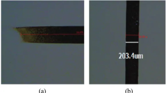
Fig. 4 shows the view of the developed pattern image of after exposure to the proton beam and developing 20min. We can see that the boundary of the patterns is not clear in the image. The reason is that when the focused proton beam passes through the slit, the edge of the slit does not become precisely aligned. The reason why the fine pattern was formed is that some protons are presumably incident by the scattering of the proton beam. We have confirmed that actual pattern size are 203.4 ㎛ width and 5 mm length or below.
(a) (b)
Fig. 3. View of the developed pattern image after exposure to the proton beam (developing time (a) 10 min (b) 15 min, line and width 5 mm and width 200㎛.
(a) (b)
Fig. 4. View of the developed pattern image after exposure to the proton beam (a), (b) line and width 5 mm and 200㎛.
(a) (b)
Fig. 5. View of the developed pattern image after exposure to the proton beam (a), (b) line and width 5 mm and 68㎛.
Fig. 5 shows the image of the developed pattern in 10 min developing for the case of 68 ㎛ width and 5 mm length slit with the proton beam fluence of 100 nC/mm
2. Developing time are split into 3, 5, 7, 10, 20 min and it becomes to develop from 10 min. We confirm that there is little difference in pattern shape above 10 min. In the left figure the boundary of the end of the pattern is not distinct.
The reason is that when the focused proton beam passed through the slit, the end of the slit is not aligned precisely.
Nevertheless, the reason why the fine pattern is formed is presumed that small amount of proton was incident.
According to the research of N. Uchiya et al, the line width is different according to proton beam fluence, it is interpreted as the same reason [14]. The width of the actual pattern size is measured to 61.56 ㎛.
4. Conclusion
We fabricated micro-sized pattern structures by scanning the proton beam. The results show the potential of proton beam as a way to produce semiconductor fabrication process.
In this study, feasibility of proton beam as a next generation lithography technique and scalable pattern can be obtained by adjusting the slit size. The technique is expected to be applied to manufacture the micro- and nano- sized structures based on this proton beam writing experimental results.
Acknowledgment
This work was supported by Proton Engineering Frontier
Project.
Direct Writing Lithography Technique for Semiconductor Fabrication Process Using Proton Beam
Journal of KSDT Vol. 18, No. 1, 2019 41