215 J. Sensor Sci. & Tech. Vol. 24, No. 4, 2015 Journal of Sensor Science and Technology
Vol. 24, No. 4 (2015) pp. 215-218 http://dx.doi.org/10.5369/JSST.2015.24.4.215 pISSN 1225-5475/eISSN 2093-7563
Ag Electrode Strain Sensor Fabrication Using Laser Direct Writing Process
Hyeonseok Kim, Jaeho Shin, Sukjoon Hong, and Seung Hwan Ko
+Abstract
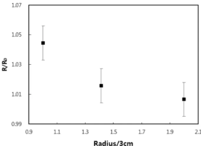
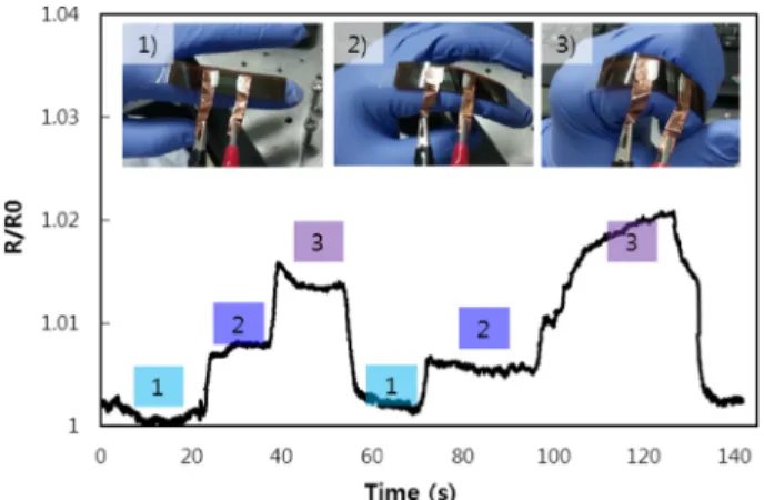
As several innovative technologies for flexible electric devices are being realized, demand for in-situ strain monitoring for flexible electric devices is being emphasized. Because flexible devices are commonly influenced by substrate strain, suitable strain sensors for flexible devices are essential for the sophisticated maneuvering of flexible devices. In this study, a flexible strain sensor based on an Ag electrode is prepared on a polyimide substrate using the LDW (laser direct writing) process. In this process, first, the Ag nanoparticles are coated on the substrate and selectively sintered using a focused laser. Because of the advantages of the LDW process (such as being mask-less, using low temperatures, and having non-vacuum characteristics), the entire fabrication process has been dramatically sim- plified; as a final outcome, a highly reliable strain sensor has been fabricated. Using this strain sensor, various strain conditions that arise from different bending radii can be detected by measuring real-time electrical signals.
Keywords: Strain sensor, Flexible device, Laser direct writing, Non-vacuum, Mask-less, Low temperature, Patterning
1. INTRODUCTION
Over the last few decades, a wide range of basic research into flexible electric devices has been conducted in diverse areas including suitable substrates for flexible devices and fabrication processes compatible with the target substrate. Currently, by virtue of the intensive progression of the last decade in both academia and industry[1], very basic flexible devices such as flexible OLEDs (organic light emitting diodes) are becoming commercially available. However, even though several flexible devices will soon be commercialized, the quality of the devices and the range of applications remain at the rudimentary level.
There are many reasons that flexible devices remain at the elementary level. One reason is that flexible substrates, which are usually made of polymers, are not compatible with standard device fabrication processes such as high temperature deposition and patterning processes using highly reactive chemicals. Because these kinds of processes have been developed in the semiconductor industry and are based on Si wafers, the majority
of fabrication processes are not compatible with polymer substrates. Therefore, to expedite flexible device development, unconventional fabrication approaches are required.
Amongst several promising candidates, LDW[2, 3] is one of the most suitable processes for flexible device fabrication. In the LDW process, a thin metal precursor layer is simply prepared on the flexible substrate using spin coating. Then, the layer is selectively sintered using a laser. Furthermore, the unsintered precursor remainders can be easily removed using normal organic solvents. Thus, patterning and fabrication do not include any costly processes demanding a vacuum, high temperatures, or toxic chemicals.
Because of these advantageous characteristics, which can be summarized as non-vacuum, low temperature, and mask-less, LDW can dramatically widen the process window and overcome the restrictions on flexible device fabrication.
Additionally, the demand for in-situ strain sensors is constantly increasing. If the sensor is flexible, the scope of applications can be greatly expanded. For example, we can utilize the sensor as a user interface by attaching it to fingers or skin.[4] Then, the sensor can convert motion into electrical signals to communicate with a computer.
Furthermore, because flexible devices and their operational characteristics are usually affected by the deformation and strain of the substrate, by integrating the device and the strain sensor, we can compensate for the effect of the strain and maneuver the device more delicately.
School of Mechanical Engineering, Seoul National University, 1 Gwanak-ro, Gwanak-gu, Seoul 151-742, Korea
+