전자빔과 무반사층이 없는 크롬 마스크를 이용한 나노그레이팅 사출성형용 고종횡비 100nm 급 니켈 스템퍼의 제작
서영호
†
· 최두선*
· 이준형*
· 제태진*
· 황경현*
Fabrication of High Aspect Ratio 100nm-scale Nickel Stamper Using E-beam Lithography for the Injection molding of Nano Grating Patterns
Young Ho Seo, Doo-Sun Choi, Joon-Hyoung Lee, Tae-Jin Je, Kyung-Hyun Whang
Key Words :
100nm Nickel Stamper(100 나노급 니켈 스탬퍼), High Aspect Ratio(고종횡비), E-beam Lithography(전자빔 노광공정), Cr/Qz Mask(크롬/퀄츠 마스크), Nickel Electroplating(니켈 도 금)Abstract
We present high aspect ratio 100nm-scale nickel stamper using e-beam lithography process and Cr/Qz mask for the injection molding process of nano grating patterns. Conventional photolithography blank mask (CrON/Cr/Qz) consists of quartz substrate, Cr layer of UV protection and CrON of anti-reflection layer. We have used Cr/Qz blank mask without anti-reflection layer of CrON which is non-conductive material and e- beam lithography process in order to simplify the nickel electroplating process. In nickel electroplating process, we have used Cr layer of UV protection as seed layer of nickel electroplating. Fabrication conditions of photolithography mask using e-beam lithography are optimized with respect to CrON/Cr/Qz blank mask. In this paper, we have optimized e-beam lithography process using Cr/Qz blank mask and fabricated nickel stamper using Cr seed layer. CrON/Cr/Qz blank mask and Cr/Qz blank mask require optimal e-beam dosage of 10.0µC/cm2 and 8.5µC/cm2, respectively. Finally, we have fabricated 116nm±6nm-width and 240nm±20nm-height nickel grating stamper for the injection molding pattern.
1. 서 론
최근 정보통신 기술의 발달로 광통신의 수요 가 급증하여, 저가의 광신호의 조작 및 제어기술 의 요구되고 있다. 이러한 광신호 조작 및 제어 기술에서 기본이 되는 것이 나노 그레이팅 구조이 다. 본 연구에서는 사출공정을 통한 나노 그레이 팅 패턴의 제작공정을 위한 니켈 스탬퍼의 제작공 정에 대해 기술하고, 전자빔과 무반사 코팅층이 없는 Cr/Qz blank mask 를 이용한 니켈 스탬퍼의 제 작공정을 제안하다.
리소그라피공정에 사용되는 크롬 마스크는 퀄
츠를 기판으로 하며, 그 위에 크롬층이 증착되어 있다. 이 크롬층은 리소그라피 공정에서 UV 의 반사를 막아주는 무반사(Anti-Reflection) 코팅층인 CrON 과 그 밑에 UV 차광막으로 사용되는 Cr(94%Cr-6%C)층으로 구성되어 있다.[1] 즉, 일반 적인 blank mask 는 PR/CrON/Cr/Qz 의 순서로 구성 되어 있다.(Fig.1(a))
CrON (Anti Reflection) : ~ 100Å Cr : ~ 650Å
Qz
Cr : ~ 750Å
Qz
(a) (b)
Fig.1 Comparison of the configuration of blank masks:
(a) Blank mask with anti-reflection layer (CrON/Cr/Qz mask); (b) Blansk mask without anti-reflection layer (Cr/Qz mask).
† 한국기계연구원 지능형정밀기계연구부 E-mail : [email protected]
TEL : (042)868-7879 FAX : (042)868-7149 * 한국기계연구원 지능형정밀기계연구부
또한, 일반적으로 도금공정을 이용하여 사출 성형용 니켈 스탬퍼를 제작하는 공정은 퀄츠나 유 리 기판위에 PR 를 코팅한 후, 레이저 직접 묘화 법이나, 전자빔 직접 묘화법으로 PR 를 패터닝하 고, PR 을 몰드로 사용하여 도금공정을 수행하게 된다.[2] 이와 같이 PR 을 몰드로 하는 니켈 도금 공정에서는 seed 의 증착이 필수적이다.
본 연구에서는 리소그라피공정에 사용되는 크 롬 마스크에 무반사 코팅층이 제거된 PR/Cr/Qz blank mask(Fig.1(b))를 사용하여 전자빔 노광공정을 최적화함으로써 크롬층을 seed 층으로 사용하여 니켈 도금공정에서 seed 층 증착공정 없이 니켈 도금을 수행하였다. 전자빔을 이용한 마스크 제 작공정은 무반사 코팅층이 있는 blank mask 를 기 준으로 설정되어 있으므로, 무반사 코팅층이 없는 경우에는 전자빔 주사량의 최적양을 다시 설정해 야 한다. Fig.2 과 Fig.3 는 각각 기존의 레이저 노 광공정을 이용한 니켈 스탬퍼의 제작공정과 무반 사 코팅층이 없는 PR/Cr/Qz mask 를 이용한 니켈 스탬퍼의 제작공정을 각각 나타낸다. Fig.3 에서 보듯이 PR/Cr/Qz mask 를 사용하면 seed 층 증착 공정없이 니켈 도금공정을 수행할 수 있다.
2. 나노 그레이팅 패턴의 설계
2.1 치수설계
본 연구에서는 먼저 무반사 코팅층인 CrON 층이 없는 Cr/Qz blank mask 를 이용하여 전자빔 리 소그라피공정을 수행하므로, 기존에 CrON/Cr/Qz blank mask 에 최적화되어 있는 전자빔 리소그라피 공정을 수정하여 Cr/Qz blank mask 에 최적화 시키 는 공정이 선행되어야 한다. 따라서, 패턴의 치수 에 따른 전자빔 주사량의 영향을 확인하기 위해서 4 가지 각기 다른 pitch 를 가진 시편을 설계하였다.
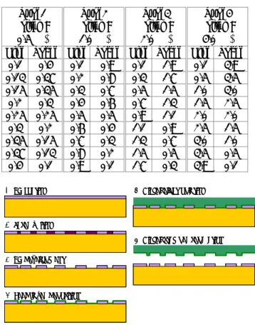
시편은 pitch(line+space) 0.5µm, pitch 1.0µm, pitch 2.0µm 그리고, pitch 4.0µm 로 각각 type1, 2, 3, 4 로 구성하였으며, type1 의 경우, line 폭은 100nm 부터 400nm 까지 Table 1 에서 보듯이 9 개 단계로 하였 고, 나머지 시편의 경우에도 각각의 pitch 에 맞게 9 단계로 line 과 space 폭을 결정하였다. Fig.4 은 설계된 시편의 개략도를 나타내며, 전체크기는 10mm×10mm 로 구성되어 있다.
Table 1. Dimension of nano-grating structure in Fig.4
Type1(pitch : 0.5 ㎛)
Type2 (pitch : 1.0 ㎛)
Type3 (pitch : 2.0 ㎛)
Type4 (pitch : 4.0 ㎛) Line Space Line Space Line Space Line Space
0.1 0.4 0.1 0.9 0.1 1.9 0.1 3.9 0.13 0.37 0.2 0.8 0.3 1.7 0.5 3.5 0.15 0.35 0.3 0.7 0.5 1.5 1.0 3.0 0.2 0.3 0.4 0.6 0.7 1.3 1.5 2.5 0.25 0.25 0.5 0.5 0.9 1.1 2.0 2.0
0.3 0.2 0.6 0.4 1.1 0.9 2.5 1.5 0.35 0.15 0.7 0.3 1.3 0.7 3.0 1.0 0.37 0.13 0.8 0.2 1.5 0.5 3.5 0.5 0.4 0.1 0.9 0.1 1.7 0.3 3.9 0.1
1. PR coating
2. Laser writing
3. PR development
4. Seed layer deposition
5. Nickel electroplating
6. Nickel stamper separation 1. PR coating
2. Laser writing
3. PR development
4. Seed layer deposition
5. Nickel electroplating
6. Nickel stamper separation
Fig.2 Fabrication process of conventional nickel stamper.
1. Cr/Quartz blank Mask
2. E-beam writing
3. PR development
4. Nickel electroplating
5. Nickel stamper separation PR/Cr = 2500Å/710Å
1. Cr/Quartz blank Mask
2. E-beam writing
3. PR development
4. Nickel electroplating
5. Nickel stamper separation PR/Cr = 2500Å/710Å
Fig.3 Fabrication process of present nickel stamper based
on Cr/Quartz mask.100130150 200250
300350 370400 100130150
200250 300350
370400
10mm
10 mm
Type 3Type 1Type 4 Type 2
100130150 200250
300350 370400 100130150
200250 300350
370400
10mm
10 mm
Type 3Type 1Type 4 Type 2
Fig.4 Schematic view of nano-grating structures.
2.2 공정설계
무반사 코팅층이 전자빔 리소그라피공정에 미 치는 영향을 확인하기 위해서 무반사 코팅층이 있 는 일반적인 CrON/Cr/Qz blank mask 와 무반사 코 팅층을 제거한 Cr/Qz blank mask 를 사용하여 각각 최적의 전자빔 주사량을 결정하고자 하였다. 전 자빔 주사량은 기존의 공정조건을 바탕으로 결정 하였으며, 6 인치 blank mask 를 이용하여 공정을 수행하였다.
3. 나노 그레이팅 패턴의 제작 및 결과
3.1 PR 몰드 제작 및 측정결과
최적의 전자빔 주사량을 결정하기 위해서 기 존의 실험을 바탕으로, PR/CrON/Cr/Qz mask 의 경 우, 9.0µC/cm2, 10.0µC/cm2, 11.0µC/cm2의 3 단계의 주사량에 대해서 실험했으며, PR/Cr/Qz mask 의 경 우에는 8.0µC/cm2, 8.5µC/cm2, 9.0µC/cm2의 3 단계의 주사량에 대해서 패터닝 실험을 수행하였다.
(x 30000 )
(a)
(x 30000 )
(b)Fig.5 SEM images of the fabricated PR mold using blank
mask and E-beam lithography: (a) PR mold on the CrON/Cr/Qz mask at 10µC/cm2; (b) PR mold on the Cr/Qz mask at 8.5µC/cm2.Fig.5 는 PR/CrON/Cr/Qz mask 와 PR/Cr/Qz mask 를 이용하여 전자빔 노광공정으로 제작된 PR 몰 드를 각각 나타내며, 설계된 치수와 제작된 치수 의 오차를 Fig.6 과 Fig.7 에 각각 나타내었다.
PR/CrON/Cr/Qz mask 의 경우, 9.0µC/cm2에서 패턴 이 덜 현상되는 under process 를 11.0µC/cm2 에서 패턴이 무너지는 over process 를 10.0µC/cm2 에서 최적의 패터닝 결과를 나타내었으며, 10µC/cm2 에 서 설계값과 비교하여 Type1 을 기준으로 최대 16nm 의 오차를 보였다.(Fig.6) PR/Cr/Qz mask 의 경우에는 8.0µC/cm2 에서 under process 를, 8.5µC/cm2에서 최적의 패턴을, 9.0µC/cm2에서 over process 를 각각 나타내었으며, Fig.7 에서 보듯이 8.5µC/cm2 에서 Type1 을 기준으로 최대 24nm 의 오차를 각각 나타내었다. 이와 같은 결과는 측정 오차를 고려할 경우, PR/CrON/Cr/Qz mask 와 PR/Cr/Qz mask 모두 적절한 패터닝 결과를 보여주 고 있음을 알 수 있다. 따라서 PR/Cr/Qz mask 를 사용하여 seed 층 증착공정없이 니켈 도금공정을 수행하여 니켈 스탬퍼 제작을 수행하였다.
Design CD [nm]
E rror CD [nm]
CrON/Cr/Qz mask
Design CD [nm]
E rror CD [nm]
CrON/Cr/Qz mask
Fig.6 Comparison of designed PR line width with
measured PR line width of type 1 specimen in the CrON/Cr/Qz mask at optimal e-beam dose of 10µC/cm2: Maximum error in type 1 is 16nm.Design CD [nm]
Er ro r C D [ n m]
Cr/Qz mask
Design CD [nm]
Er ro r C D [ n m]
Cr/Qz mask
Fig.7 Comparison of designed PR line width with
measured PR line width of type 1 specimen in the Cr/Qz mask at optimal e-beam dose of 8.5µC/cm2: Maximum error in type 1 is 24nm.(a)
(b)
(c)
(d)
Fig.8 SEM image of the fabricated nickel stamper using
Cr/Qz mask: (a) Type 1 : 0.5µm-pitch, CDmin=0.1µm, CDmax=0.4µm; (b) Type 2 : 1.0µm -pitch, CDmin=0.1µm, CDmax=0.9µm; (c) Type 3 : 2.0µm -pitch, CDmin=0.1µm, CDmax=1.9µm; (d) Type 4 : 4.0µm -pitch, CDmin=0.1µm, CDmax=3.9µm.3.2 Nickel Stamper 제작 및 측정결과
제작된 PR 몰드용 PR/Cr/Qz mask 의 Cr 층이 100Ω의 저항을 나타내었다. 100Ω의 저항으로 인 해 니켈 도금공정시 seed 층으로 작용하는 Cr 이 전기적 데미지를 받았다. 100Ω의 저항은 본 연구 에서 사용된 PR/Cr/Qz mask 의 70nm 의 Cr 층 두께 가 너무 얇음을 의미한다. 니켈 도금공정을 수행 하기 위해 120nm 의 니켈을 추가적으로 증착을 수 행하여 10Ω이하의 저항을 얻었다. 추후 공정에서 는 Cr 두께를 250nm 이상 증착한 PR/Cr/Qz mask 를 사용한다면 추가적인 seed 층 증착공정없이 니 켈도금을 수행할 수 있을 것이다. Fig.8 은 이와 같이 제작된 type1,2,3,4 니켈 스탬퍼의 SEM 사진 을 나타낸다..
Fig.9 는 제작된 니켈 스탬퍼의 두께를 측정하 기 위해 AFM 측정을 수행한 결과를 나타내며, 측 정된 두께는 약 240±20nm 로 초기 PR 몰드 두께 인 250nm 와 거의 일치함을 알 수 있다. AFM 측 정에서 선폭이 완벽하게 나타나지 않은 것은 종횡 비가 3 에 가까운 시편이라 AFM tip 이 정확이 측 정 못한 결과이다. 제작된 니켈 스탬퍼의 두께를 측정한 결과를 PR 몰드 치수와 비교한 결과를 Fig.10 에 나타냈으며, type1 을 기준으로 20nm 의 오차를 나타내었다.
Fig.9 AFM image of the fabricated nickel stamper of
type 4: The height of the nickel stamper is 240nm±20nm.Fig.10 Comparison of PR mold line width with nickel
stamper line width of type 1 specimen in the Cr/Qz mask at optimal e-beam dose of 8.5µC/cm2: Maximum error in type 1 is 20nm.4. 결론
본 연구에서 전자빔 노광공정과 마스크제작공 정을 사용하여 seed 층 증착없이 니켈 스탬퍼를 제 작하는 방법을 제안하였으며, 실험적으로 무반사 층이 없는 PR/Cr/Qz mask 의 최적 노광조건을 확 립하였다. 또한 PR/Cr/Qz mask 를 사용하여 종횡 비 2.5 의 100nm 급 그레이팅 니켈 스탬퍼를 제작 완료하였다. 본 연구에서 제안한 니켈 스탬퍼의 제작공정은 기존의 니켈 스탬퍼의 제작공정을 단 순화하였고, 향후 사출공정을 이용하여 나노 그레 이팅 패턴의 저가생산에 기여할 것이다.
후 기
본 연구는 과학기술부의 21 세기 프론티어 사업의 일환인 “나노메카트로닉스 기술개발사업”의 지원 으로 수행되었습니다.
참고문헌
(1) G. Timp, Nanotechnology, Springer. 1999.
(2) G. T.A. Kovacs, Micromachined Transducers, McGraw-Hill,