Progress in Superconductivity Vol.10 No.2 pp.99-102 30 April 2009
- 99 -
Fabrication of Sub-Micron Size Al-AlO
x-Al Tunnel Junction using Electron-Beam Lithography and Double-Angle Shadow
Evaporation Technique
M. Rehman
a,b, J. W. Choi
c, S. J. Ryu
c, J. H. Park
a,d, S.-W. Ryu
b, Z. G. Khim
d, W. Song
a, Y. Chong
*,aa Korea Research Institute of Standards and Science, Daejeon, Korea
b Department of Physics, Chonnam National University, Gwangju, Korea
c Department of Physics, KAIST, Daejeon, Korea
d Department of Physics, Seoul National University, Seoul, Korea (Received 3 March 2009; revised 27 March 2009; accepted 30 March 2009)
전자빔 패터닝과 double-angle 그림자 증착법을 이용한 sub-micron 크기의 Al-AlO
x-Al 터널접합 제작공정개발
M. Rehman
a,b, 최재원
c, 류시정
c, 박정환
a,d, 류상완
b, 김정구
d, 송 운
a, 정연욱
*,aAbstract
We report our development of the fabrication process of sub-micron scale Al-AlOx-Al tunnel junction by using electron-beam lithography and double-angle shadow evaporation technique. We used double-layer resist to construct a suspended bridge structure, and double-angle electron-beam evaporation to form a sub-micron scale overlapped junction. We adopted an e-beam insensitive resist as a bottom sacrificing layer. Tunnel barrier was formed by oxidation of the bottom aluminum layer between the bottom and top electrode deposition, which was done in a separate load-lock chamber. The junction resistance is designed and controlled to be 50 Ω to match the impedance of the transmission line. The junctions will be used in the broadband shot noise thermometry experiment, which will serve as a link between the electrical unit and the thermodynamic unit.
Keywords : Tunnel junction, Shadow evaporation, E-beam lithography
I. Introduction
Tunneling effect is a quantum phenomenon that
*Corresponding author. Fax : +82 42 868 5018 e-mail : [email protected]
100 M. Rehman et al.
can be observed in a classical measurement. In case of metal to metal tunneling, a very thin and uniform insulating barrier is necessary. Natural aluminum oxide has provided the best tunneling barrier where we use aluminum as one of the electrode [1, 2].
Metal tunnel junctions have been used in the study of superconducting phenomena, and recently in the study of magnetic tunnel junction for spintronic devices. Very small tunnel junctions were used in studying single electron tunneling effect [3]. The tunneling transport will reflect the thermal broadening of the Fermi function, so when we measure the current noise across a tunnel junction, we can calculate the electronic temperature of the junction [4]. For this noise thermometry purpose, we have developed a fabrication process of sub-micron size Al-AlOx-Al tunnel junction.
In AlOx barrier tunnel junctions, several parameters can control the junction properties.
Oxygen pressure and oxidation time during oxidation, the junction size, and surface morphology will affect the quality of the tunnel barrier. We will measure small noise signal from our junction, preferably at high frequencies over RF bandwidth. Therefore, in order to get the maximum coupling of the signal to the measurement leads, especially when we want to use a broadband signal, it is preferable to have an impedance match between the sample and the transmission line, that is, 50 Ω.
Fig. 1. Design of our junction layout. At the center the suspended bridge will be formed.
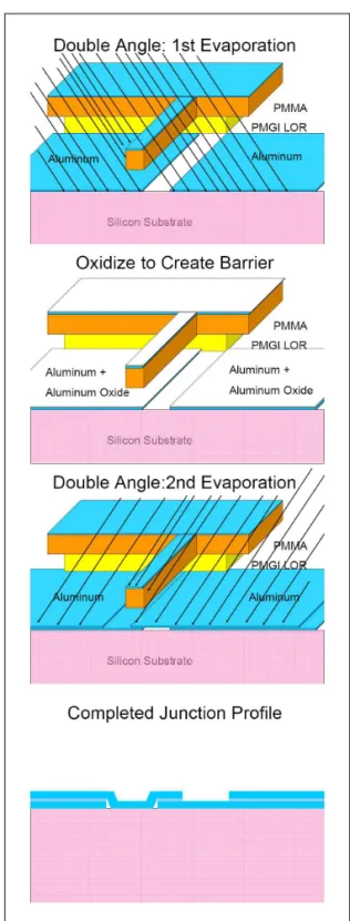
Fig. 2. Fabrication process for tunnel junction devices using double-angle evaporation is shown. Substrate is tilted away from stream of evaporated aluminum during first evaporation. After oxidation of Al surface, the substrate is tilted in the other direction and aluminum is evaporated again.
Fabrication of Sub-Micron Size Al-AlOx-Al Tunnel Junction.... 101
II. Fabrication method
We use double-layer resist to form a suspended bridge structure as a shadow mask. In our previous process we used co-polymer/PMMA double layer for resist. But since the co-polymer is photoreactive, it is often difficult to control the e-beam dose to match both PMMA and co-polymer to get a desired structure. We changed the bottom lift-off resist to e-beam insensitive LOR10B(Microchem) [5], while PMMA is still used as the top imaging resist.
First the lift-off resist LOR10B is coated on an oxidized silicon substrate at 3200 rpm, which results in 1 μm thick resist. This resist does not react with UV or e-beam, but can be easily removed in developer like MF320. On top of LOR10B, PMMA-C4 is spin- coated, which will serve as the e-beam resist. First the PMMA is patterned by e-beam, and developed in MIBK:IPA(1:1) developer. This PMMA pattern serve as a wet-etch mask for LOR10B. Electron- beam lithography was done in field-emission scanning electron microscope (SEM, FEI Sirion) with a control software by Raith Co. GDS format file can be directly applied to expose the pattern.
We use two different electron beam dose for different regions of the pattern with different minimum feature size. Then undercut is formed by resolving LOR10B in MF320 developer, where the PMMA pattern will serve as wet-etch mask. By controlling the etch time, we control the shape of the undercut in the desired form. A narrow suspended bridge is formed by the remaining PMMA bar where LOR10B under the bridge is completely etched out.
The patterned suspended bridge structure is shown in Fig. 3(a). This suspended bridge is the shadow mask for the angle evaporation [6].
Aluminum deposition is done by electron-beam evaporation. Base pressure of the deposition chamber is kept at 1×10⁻⁸ torr, while the pressure rises to 3×10⁻⁸ torr during evaporation. The thickness of each aluminum layer is monitored by crystal thickness
monitor. We use 30 nm thick Aluminum for the bottom and the top layer. The first aluminum layer is deposited at an angle of +40° from the substrate normal. After the bottom electrode deposition, the sample is brought to the separate load-lock chamber and oxidized for 3 minutes at 0.2 torr of oxygen pressure. Then the sample is brought back to the main chamber and the top electrode is deposited at an angle of -40°. By controlling the angle, we can control the overlap width, hence the junction size.
(a)
(b)
Fig. 3. (a) Picture of the patterned resist is shown with suspended bridge in the center (inset:SEM picture of the suspended bridge) (b) Picture of fabricated tunnel junction is shown. The overlapped region is the junction whose size is about 10 μm wide and 0.5 μm long.
102 M. Rehman et al.
After metal deposition, the film was soaked in acetone for several hours for lift-off. Junction resistance is checked on the probe station by 2-probe method, and then the chip is mounted on a chip holder. Contacts are made by ultrasonic wedge bonder for 4-probe measurement. Zero bias resistance is checked at 1μA current level. Junctions are measured at low temperature down to liquid helium temperature. Selected test junctions are measured up to high bias of several hundred mV for reliability check. We mainly fix the deposition angle and control the oxidation process to get the desired resistance value.
III. Results and discussion
Fig. 3(b) shows a photo of the fabricated tunnel junction. The junction size is 10 μm wide and 0.5 μm overlap. The width of the junction is chosen to get a reasonable impedance of 50 Ω under our oxidation condition. Typical 2-probe resistance values of the fabricated junction at room temperature lie between 20 and 80 Ω. In terms of the fabrication yield, the resistance values of 10 junctions out of 20 consecutively-fabricated junctions fall into this range.
One of the main problem that caused the run-to- run scatter of the junction parameter is the detailed shape of the suspended bridge, where collapsing of the bridge sometimes occurs during wet-etching of LOR10B. This is controlled by using different electron beam dose in regions with different minimum feature size.
One junction with a resistance of 40 Ω was able to sustain maximum current of 10 mA and voltage of 400 mV at 4 K before the tunnel barrier breaks down.
In unstable junctions, junction resistance showed sudden jump to a higher value during measurement.
This is supposed to be caused by burning of micro-
short channels in imperfect junction barrier. In some junctions, the junction resistance increase by about 10 % after a thermal cycle to liquid helium temperature. This also indicates an imperfect tunnel junction formation. Since we will need reliable and robust tunnel junctions for noise thermometry experiment, this I-V measurement and pre-thermal cycling serve as a screening process of imperfect junctions, so that only good junctions can be used in serious low temperature measurements with He-3 or dilution refrigerator. Low temperature measurements below 1 K will be performed with selected good junctions.
In summary, we setup a fabrication process for Al-AlOx-Al tunnel junction devices using double- angle evaporation technique with PMMA/LOR10B double-layer resist and electron-beam lithography patterning. Detailed properties of the junctions are under investigation.
Acknowledgments
We express our sincere thank to the members of Center for Nanoscience and Quantum Metrology of KRISS.
References
[1] M. Gurvitch, M. A. Washington, H. A. Huggins, Appl.
Phys. Lett. 42, 472 (1983).
[2] W. F. Brinkman, R. C. Dynes, J. M. Rowell, J. Appl.
Phys. 41, 1915 (1970).
[3] H. Grabert and M. H. Devoret, Eds., Single Charege Tunneling, Plenum Press, London (1991).
[4] L. Spietz, K. W. Lehnert, I. Siddiqi, R. J. Schoelkopf, Science 300, 1929 (1999).
[5] LOR and PMGI Resists datasheet, Microchem.
[6] G. J. Dolan, Appl. Phys. Lett. 31, 337 (1977).