Vol. 30, No. 10 (2020)
509
Simulation on Optimum Doping Levels in Si Solar Cells
Kwang Su Choe
†Dept. of Electronic Materials Engineering, College of Engineering, The University of Suwon, Hwaseong-Shi, Gyeonggi-Do 18323, Republic of Korea
(Received October 16, 2018 : Revised September 11, 2020 : Accepted October 5, 2020)
Abstract
The two key variables of an Si solar cell, i.e., emitter (n-type window layer) and base (p-type substrate) doping levels or concentrations, are studied using Medici, a 2-dimensional semiconductor device simulation tool. The substrate is p- type and 150 µm thick, the pn junction is 2 µm from the front surface, and the cell is lit on the front surface. The doping concentration ranges from 1 × 1010 cm−3 to 1 × 1020 cm−3 for both emitter and base, resulting in a matrix of 11 by 11 or a total of 121 data points. With respect to increasing donor concentration (Nd) in the emitter, the open-circuit voltage (Voc) is little affected throughout, and the short-circuit current (Isc) is affected only at a very high levels of Nd, exceeding 1 × 1019 cm−3, dropping abruptly by about 12%, i.e., from Isc = 6.05 × 10⁻⁹ A·µm−1, at Nd = 1 × 1019 cm−3 to Isc = 5.35 × 10⁻⁹ A·µm−1 at Nd = 1 × 1020 cm−3, likely due to minority-carrier, or hole, recombination at the very high doping level. With respect to increasing acceptor concentration (Na) in the base, Isc is little affected throughout, but Voc increases steadily, i.e, from Voc = 0.29 V at Na = 1 × 1012 cm−3 to 0.69 V at Na = 1 × 1018 cm−3. On average, with an order increase in Na, Voc increases by about 0.07 V, likely due to narrowing of the depletion layer and lowering of the carrier recombination at the pn junction. At the maximum output power (Pmax), a peak value of 3.25 × 10⁻² W· cm−2 or 32.5 mW· cm−2 is observed at the doping combination of Nd = 1 × 1019 cm−3, a level at which Si is degenerate (being metal-like), and Na = 1 × 1017 cm−3, and minimum values of near zero are observed at very low levels of Nd ≤ 1 × 1013 cm−3. This wide variation in Pmax, even within a given kind of solar cell, indicates that selecting an optimal combination of donor and acceptor doping concentrations is likely most important in solar cell engineering.Key words
Si solar cell, front-lit cell, solar cell doping, carrier recombination, Medici.1. Introduction
In the sense that the photovoltaic power generation is driven by the potential energy of electrons elevated by absorbing sun light, it is akin to hydroelectric power generation where the energy source is the potential energy of water molecules elevated by absorbing heat from the same sun light. A solar cell, or a pn junction, where the photovoltaic effect takes place should thus share many common physical attributes with a hydroelectric dam or a waterfall. In another words, the attributes that make a waterfall great should also apply to a pn junction.
The pn junction being invisible to naked eyes, this waterfall analogy is very useful in understanding and visualizing the workings of a pn junction and has been used in the past by the present author.
1)To maximize the use of potential energy, a waterfall must have a high elevation and a stiff drop, or respectively a pn junction must have a high barrier height and a narrow depletion layer. To maximize flow, a waterfall needs hard bedrocks preventing water seepage, or a pn junction needs defect-free materials preventing carrier loss by recombination. All these three attributes concerning the pn junction, i.e., barrier height, depletion layer, and carrier recombination, are affected by the doping levels in the p- and n-type regions. In theory, a higher doping level, in both the p- and n-type regions, leads to a higher barrier height and a narrower depletion layer, but not a lower carrier recombination. Thus, an optimum doping level or a combination of doping levels needs to be defined to satisfy these diverging requirements.
An issue key to understanding proper doping is solar
†Corresponding author
E-Mail : [email protected] (K. S. Choe, Univ. Suwon)
©Materials Research Society of Korea, All rights reserved.
This is an Open-Access article distributed under the terms of the Creative Commons Attribution Non-Commercial License (http://creative- commons.org/licenses/by-nc/3.0) which permits unrestricted non-commercial use, distribution, and reproduction in any medium, provided the original work is properly cited.
cell design. Currently, the prevailing Si solar cell design is front-lit or front-junction where the pn junction is formed very near the front surface that faces the sun. In its fabrication, the substrate (base) is usually doped p- type, and on it a thin layer of n-type window layer (emitter) is formed by thermal diffusion. For electrodes, thin grid lines of cathode, usually of Al or Ag, are deposited on the n-type window layer, and a full anode layer, usually of Al, is deposited on the rear (substrate).
In this solar cell structure, the relative levels of doping concentration in the p- and n-type regions are closely linked with the relative thicknesses of the p- and n-type regions. That is, the p-type region which is at a higher energy level needs to be relatively much thicker, so that more light absorption, or free electron-hole pair generation, takes place in that region as much as possible. So, the substrate itself is usually chosen as p-type. On this substrate, the n-type window layer is formed by doping to the degenerate level, i.e., above 1×10
18cm
−3, so that it can be made as thin as possible and, at the same time, does not have any carrier depletion.
An added benefit in having p-type substrate is that the minority carriers are electrons that diffuse faster than holes, resulting in less minority-carrier recombination in the substrate. Had the substrate been n-type, the minority- carrier holes would be more prone to recombination due to their slower speed. A drawback in using the p-type substrate is light-induced degradation (LID) known to exist in the p-type Czochralski (CZ) silicon associated with boron-oxygen complexes.
2)The Si substrate, the p- type region, is usually doped to a much lesser degree than the n-type layer, mainly to prevent carrier depletion in the latter layer and also to minimize minority-carrier recombination within itself.
In regards to energy conversion efficiencies, for front- lit Si solar cells, the highest efficiency reported to date for an actual cell is 24.7 % by a method known as PERL (Passivated Emitter, Rear Locally-diffused),
3)while the more typical value accepted in laboratory-scale solar cells is about 20 %, or 20 mW·cm
−2under AM1.5.
4)In production, the efficiency further drops to 17 ~ 18 %, which calls for improvement. Together with substrate and window layer thicknesses, the respective doping levels are two key variables directly influencing the solar cell performance - the energy conversion efficiency and ultimately the power output. The extent of their influence is one that needs to be studied comprehensively.
Typical doping levels used in the industry is approximately 1.5×10
16cm
−3(1 Ω·cm) for the base and 3 × 10
19cm
−3peak (100 Ω/sq) for the emitter. These values, derived experimentally, are not always necessarily optimal for evolving Si substrate designs. In the field of computer simulation, optimization has been generally done utilizing
PC1D, a widely used 1-dimensional solar cell software.
A recent PC1D study indicates an optimal base doping range of Na = 1.84×10
17- 2.68×10
17cm
−3at a fixed emitter doping level of Nd = 7.5×10
18cm
−3for 300 ~ 320 µm thick Si substrates.
5)Due to limited doping ranges reported thus far, a more expanded study is being called for.
In this work, a computer simulation study was conducted in lieu of laboratory experiments by using a 2- dimensional semiconductor device simulation software package called Medici.
6)Despite limitations of computer simulation, the results will show by means of quantitative trends in key performance factors, such as short-circuit current, open-circuit voltage, and maximum power output, the most desirable combination of p- and n-type doping concentrations in Si solar cells.
2. Experimental Procedure
In computer simulation, the computer is a virtual laboratory. That is, the solar cell fabrication is moved from a real laboratory into the computer. When an experiment was to be repeated many times to the extent that it is not practically possible in a real laboratory, the mathematical modeling and computer simulation is a viable alternative. A graphic version of a solar cell is made in the virtual space step by step, emulating the fabrication steps in a real laboratory, and an essential variable or variables can be tested and investigated in iterative manner. In this study of Si solar cells, two essential variables are emitter (n-type window layer) and base (p-type substrate) doping concentrations.
For simulation, the 2-dimensional version of Medici, a well-known semiconductor device simulation software tool, was utilized. As in any device simulation, the Medici simulation consists of four major steps. First, the solar cell structure is formed by a grid or mesh, sort of like constructing a modeled building using match sticks.
The regions near the front and back surfaces and at the pn junction where active photo-generation and/or carrier transport occur are finely meshed, and the bulk region deep in the body of the solar cell, where the electrical activities are relatively steady and not as much space- dependant, is coarsely meshed to save computation time.
Each type of the p- and n-type regions is then doped to a desired level. Second, the physical models, expressed in differential equations, relating to the operation of the solar cell and the mathematical methods of solving them are each specified. Third, the solutions are reached by iterative numerical calculations. Fourth, the simulation results or the outputs are accessed in texts, plots or figures.
For the simulation, a standard 2-dimensional back-lit
grid structure in the Medici operational manual
6)is modified to fit the front-lit design. In this front-lit structure, the substrate is 150 µm thick and doped p-type, and the window layer is 2 µm thick and doped n-type.
Thus, the location of the pn junction is 2 µm below the front surface. Laterally, only a 10µm segment of the substrate is defined to conserve the simulation time. The front electrode (cathode) is 1µm wide and centered on this 10 µm segment, and the back electrode (anode) covers the whole rear surface. The said grid structures had been used successfully and illustrated in earlier studies.
7,8)The doping concentration, the experimental variable, ranges from 1×10
10cm
−3to 1×10
20cm
−3for both the substrate and the window layer. Thus, a matrix of 11 by 11, or a total of 121 data points, was experimented in the simulation study.
On physical models, the Auger and concentration- dependent Shockley-Read-Hall recombination models and the concentration-dependent mobility model are chosen. On equation solving, the 2-carrier Newtonian iteration is chosen as the mathematical method in solving the governing differential and continuity equations by finite element analysis. The information on thermal processing conditions, which is important in fabrication as it affects the pn junction formation, is not an input variable in Medici which is a device-level simulator.
The minority-carrier recombination lifetime is fixed at 5×10
−5s or 50 µs for free electrons. In common Si solar cell materials, the minority-carrier recombination lifetime ranges approximately from 1 ms to 1ns: the longest lifetime belonging to float-zone (FZ) silicon, followed by Czochralski (CZ) silicon and then polycrystalline silicon.
Specifically, the electron recombination lifetime (τ
n) in the p-type Si substrate is about 5 ms as grown and about 550 µs after oxidation for float-zone (FZ) type, 2.5 ms as grown and about 550 µs after oxidation for magnetic Czochralski (MCZ) type, and about 550 µs as grown and about 100 µs after oxidation for normal CZ type.
9)In previous simulation, this 50 µs electron lifetime value was found to be the minimum required for the front-lit solar cell formed on a 150 µm thick p-type Si substrate.
8)Here, a longer lifetime means less defects in the material as the defects tend to hinder the movement of a minority carrier and increase the chance that it is captured and recombines with a majority carrier. The FZ method, because it is contactless, produces the highest quality Si crystals, while the CZ method, where Si melts contact SiO
2crucible, produces reasonably good quality Si crystals that contain some defects associated with dissolved oxygen. The lifetime for holes (τ
p) is not at issue as long as it is longer than 50 ns because the holes have short distance to travel in the thin n-type window layer.
8)As such, it is also
fixed at 50 µs. Lastly, except for the parameters that have been discussed, default values are used for all others.
The photo-generation rate, electron-hole-pairs·cm
−3·s
−1, is an exponential function of distance y from the surface and can be expressed as
(1) where FLUX is defined as the photon flux (photons·cm
−2· s
−1) and Y.CHAR is defined as the absorption distance (µm).
6)The photon absorption is strongly frequency- dependent. That is, higher the frequency, or shorter the wavelength, the stronger the photon absorption and therefore the shorter the absorption distance. For the present simulation experiments, the wavelength of 0.6 µm, the peak point in the AM1.5 spectrum having an absorption distance of 2 µm, is chosen for the incident photons. The photon flux, directed normal to the surface, is set at 4×10
17cm
−2·sec
−1. For these absorption distance and photon flux, the Eq. (1) can be rewritten as
(2) Finally, after the simulation, the output is plotted in terms of the photovoltaic equation as expressed in
(3) From the I-V curve plotted, the open-circuit voltage, V
OC, is extracted from where the curve intersects the x- axis, and the short-circuit current, I
SC, is extracted from where the curve intersects the y-axis. The cell power as defined by the maximum power rectangle in a loaded circuit is then extracted.
3. Results and Discussion
The grid structure of the front-lit Si solar cell formed in Medici is illustrated in Fig. 1. The front and back electrodes and the sun are added to the figure. As the absorption distance, i.e., the distance at which the intensity of the light is decreased to 1/e of the initial value, is 2 µm for the 0.6 µm wavelength light used in the simulation, the 63 %, 86 %, and 95 % of the incident photons would be absorbed within one, two and three absorption distances or 2 µm, 4 µm, and 6 µm from the front surface, respectively. Thus, the most of light absorption, or free electron-hole pair generation, takes place within the distance of 6 µm from the front surface, or mostly near the pn junction. Since the generation sites are not very far from the pn junction, the minority-carrier
CHAR Y
CHAR Y
y FLUX
G
photon. 10
exp .
4
× ⎥⎦ ⎤
⎢⎣ ⎡ −
=
−1 3 2
21
sec
10
2
− −−
−
×
= e cm
G
my
photon µ
kT sc qV
o
e I
I
I = ( − 1 ) −
recombination should not be significant except at the pn junction where the two minority carriers meet. In this regard, the grid in Fig. 1 is dense near the front surface and more so at the pn junction.
Effects of n-type emitter doping or donor concentration
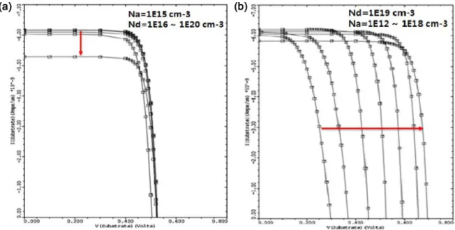
(Nd) and p-type base doping or acceptor concentration (Na) viewed separately are illustrated in Figs. 2(a) and 2(b), respectively. With regard to increasing donor con- centration, for a fixed acceptor concentration, Fig. 2(a) shows that the open-circuit voltage (Voc) is little affected
Fig. 1. The 10 µm × 150 µm grid structure of the front-lit Si solar cell formed by Medici: the pn junction is located at 2 µm below the top (front) surface, the p-type substrate is 150 µm thick, and the top electrode is 1µm wide and centered on the n-type window layer (the x- and y-axis labels indicate distance in microns).
Fig. 2. The I-V characteristics of the front-lit Si solar cell: (a) increasing donor concentration (Nd) while acceptor concentration (Na) is fixed and (b) increasing Na while Nd is fixed (the x-axis label indicates substrate voltage in volts, and the y-axis label indicates substrate current in 10−9 A·µm−1).
throughout and that the short-circuit current (Isc) is affected only at a very high donor concentration exceeding 1×10
19cm
−3, where it drops abruptly by about 12%, i.e., from Isc = 6.05×10
−9A·µm
−1at Nd = 1×10
19cm
−3to Isc
= 5.35×10
−9A·µm
−1at Nd = 1×10
20cm
−3. This indicates that the minority-carrier, or hole, recombination in the emitter layer is not an issue up until the very high doping level. The near constancy in open-circuit voltage indicates that the depletion region at the pn junction is mostly all formed in the p-type base and as such any additional donor doping in the n-type emitter has little effect.
With regard to increasing acceptor concentration, for a fixed donor concentration, Fig. 2(b) shows that the short- circuit current is little affected throughout, but the open- circuit voltage increases steadily. i.e., from Voc = 0.29 V at Na = 1×10
12cm
−3to Voc = 0.69 at Na = 1×10
18cm
−3. On average, per an order increase in acceptor concentration, the open-circuit voltage increases by about 0.07 V, indicating the narrowing of the depletion layer and the lowering of the carrier recombination at the pn junction.
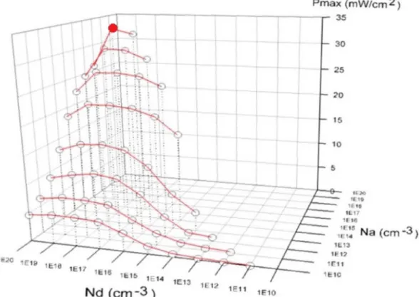
The overall effect of donor and acceptor doping on the maximum output power (Pmax) is illustrated in Fig. 3.
Of the 121 data points in the 11×11 matrix experimented, no viable solution was reached when Na ≥ Nd or Na ≥ 1×10
19cm
−3, i.e., situations where the 2 µm n-type layer is likely becoming depleted of carriers, and the good data
points collected are plotted in the figure. In this three- dimensional illustration resembling a graded hill, a ridge leading up to the peak is visible along the donor concentration of 1×10
19cm
−3, a level at which Si is degenerate (being metal-like). The peak is reached when the acceptor concentration is increased to 1×10
17cm
−3. The maximum output power at this peak point of Nd = 1×10
19cm
−3and Na = 1×10
17cm
−3is 3.25×10
−2W·cm
−2or 32.5 mW·cm
−2. The maximum output power is near zero near the base of the hill where Nd ≤ 1×10
13cm
−3. This elevation from zero to 32.5 mW·cm
−2in the maximum output power indicates that a wide range of power output is possible even for a given kind of solar cell and that selecting an optimal combination of donor and acceptor doping concentrations is likely most important in solar cell engineering.
Of the two doping parameters, the donor doping in the emitter was less robust than the acceptor doping in the base in influencing the output power, as indicated by the gentler slopes on the donor side (Nd) of the 3-dimensional hill in Fig. 3. This is because the emitter itself is much thinner than the base, which in effect allows photon- generated minority carriers (holes) to diffuse out of the emitter faster and be less affected by the presence of doped majority carriers (conduction electrons) nearby.
A note of caution is that the optimal doping combination
Fig. 3. Maximum output power (Pmax) as a function of donor concentration (Nd) and acceptor concentration (Na). The peak value (solid red dot) is 32.5 mW·cm−2 at Nd = 1×1019 cm−3 and Na = 1×1017 cm−3.
leading to the maximum power output is not absolute, but relative to other solar cell parameters, such as minority- carrier recombination lifetime and substrate quality and thickness. In an earlier study, it was shown that an output power loss is expected if electron recombination lifetime is shorter than 50 µs.
8)It is also known that the substrate thickness and the required minority-carrier recombination lifetime are nearly linearly related, i.e., the thicker the substrate, the longer the lifetime. These results indicate that the substrate doping should be made lower for lower quality silicon substrates having shorter minority-carrier recombination lifetimes or that it could be made higher for thinner substrates. Thus, the optimal doping combination found in this study should be used as a guide and adjusted according to changing conditions. The experimental verification of the findings made in this study is left for the future study.
4. Conclusions
The relationship between two key variables of the Si solar cell, i.e., emitter (n-type window layer) and base (p- type substrate) doping levels or concentrations, was studied by using Medici, a 2-dimensional semiconductor device simulation tool. The doping concentration, the experimental variable, ranged from 1×10
10cm
−3to 1×10
20cm
−3for both the window layer and the substrate.
Thus, a matrix of 11 by 11, or a total of 121 data points, was experimented. With respect to increasing donor concentration (Nd) in the n-type window layer (emitter), the open-circuit voltage was little affected throughout, and the short-circuit current was affected only at a very high donor concentration exceeding 1×10
19cm
−3, where it dropped abruptly by about 12 %, indicating that the minority carrier, or hole, recombination in the emitter layer was not an issue up until the very high doping level. With respect to increasing acceptor concentration (Na) in the p-type substrate (base), the short-circuit current was little affected throughout, but the open-circuit voltage was greatly affected, i.e., on average increasing by about 0.07 V per an order increase in acceptor concentration, possibly due to narrowing of the depletion layer and the lowering of the carrier recombination at the pn junction. On the maximum output power. a peak value of 3.25×10
−2W·cm
−2or 32.5 mW·cm
−2was observed at the doping combination of Nd = 1×10
19cm
−3, a level at which Si is degenerate (being metal-like), and Na =
1×10
17cm
−3, while minimum values of near zero were observed at very low doping combinations. This wide variation even for a given kind of solar cell indicates that selecting an optimal combination of donor and acceptor doping concentrations is likely most important in solar cell engineering. The optimal doping values of Nd = 1×10
19cm
−3and Na = 1×10
17cm
−3found in this work for Si substrate thickness of 150 µm and minority-carrier recombination lifetime of 50 µs are left for verification in future experimental studies.
Acknowledgement
The simulation experiments and the rendering of the graphical work were assisted by undergraduate students, Messrs. Sang-Hoon Lee, Jong-Min Moon, Ji-Min Kim and Misses In-Young Kim, Yeh-Lim Bang, Soo-Hyeon Sohn, Mi-Jin Sohn of the Department of Electronic Materials Engineering of the University of Suwon. The author wishes to thank them for their diligent assistance.
This paper was supported by the research grant of the University of Suwon in 2017.
References
1. K. S. Choe, Korean J. Mater. Res., 27, 107 (2017).
2. V. G. Weizer, H. W. Brandhorst, J. D. Broder, R. E. Hart and J. H. Lamneck, J. Appl. Phys., 50, 4443 (1979).
3. M. A. Green, K. Emery, D. L. King, Y. Hishikawa and W. Warta, Prog. Photovoltaics, 15, 35 (2007).
4. J. H. Kim, M. J. Chu, Y. D. Chung, R. M. Park and H.
K. Sung, Electron. Telecommunications Trends, 23, 2 (2008) (in Korean).
5. S. T. Ferdiansjah and D. Faridah, ARPN J. Engr. and Appl. Sci., 11, 4011 (2016).
6. Medici Two-Dimensional Device Simulation Program, ver. 2.2, User's Manual, vol. 3, p. 7.1-7.10, Technology Modeling Associates, Inc., Sunnyvale, CA (1996).
7. K. S. Choe, Solid State Sci., 29, 48 (2014).
8. K. S. Choe, Korean J. Mater. Res., 28, 38 (2018).
9. S. K. Pang, A. Rohatgi, B. L. Sopori and G. Fiegl, J.
Electrochem. Soc., 137, 1977 (1990).
Author Information
최광수
수원대학교 전자재료공학과 교수