1. Introduction
Solar cell technology depended on efficiency, operational stability and its production cost as three of the most important factors that determined viability of a photovoltaic (PV) technology. The initial efficiency determined the available output power from the device under standard illumination condition, while its characteristic stability profile provided the predicted efficiency in future time scale, and the stability depended on various factors as well. Cost of the module determined acceptability of the device for its large-scale application or use. In the past, a combination of the higher price of the device, lower efficiency and stability made most of the devices not so popular for renewable energy sources. But the things had been changing rapidly and it was foreseeable that more stable, efficient and reduced cost solar cells would be available in future. The progress was taking place in many fronts.
Crystalline Si (c-Si) based solar cells showed a Jsc more than 40 mA/cm2 but its open circuit voltage (Voc) remained low. It might be possible to improve the Voc by using such a solar cell in a tandem structure with a wide Eg thin film silicon1-3), compound4,5), organic polymer or perovskite cell6,7) at the top.
The advantage of such a cell structure was that the overall performance of the tandem cell improved. That was to make PV modules with higher efficiency than market-leading c-Si while leveraging existing c-Si manufacturing capacity, Si-based tandem approaches had been proposed1-7). Looking into the successful operational principle of two terminal tandem solar cells, spectrum splitting and four terminal tandem cells were also investigated. In the spectrum splitting, the incident radiation was divided into multiple optical beams having desired bands of wavelength. These beams were then incident on specific solar cells that were optimized for those optical bands8-10). Recently four terminal Si based tandem solar cells with a top perovskite sub-cell were investigated that shows a 24.6% efficiency11).
In this paper, the results of research on multi-junction solar cells with thin film a-SiGe:H solar cells and c-Si solar cell tandem junctions were studied.
2. Experimental
A commercial Czochralski-grown n-type waferd (resistivity of 2.7 Ω·cm, thickness of 200 μm) was used as an absorber material for the bottom cell on Si based multi junction solar cell.
The typical sequence was pre-texture cleaning texturization and
DOI:https://doi.org/10.21218/CPR.2020.8.3.094 eISSN 2508-125X
Thin Film Si-Ge/c-Si Tandem Junction Solar Cells with Optimum Upper Sub- Cell Structure
Jinjoo Park*
Major of Energy and Applied Chemistry, Division of Energy & Optical Technology Convergence, Cheongju University, Cheongju-si 28503, Korea
Received September 9, 2020; Accepted September 14, 2020
ABSTRACT: This study was trying to focus on achieving high efficiency of multi junction solar cell with thin film silicon solar cells. The proposed thin film Si-Ge/c-Si tandem junction solar cell concept with a combination of low-cost thin-film silicon solar cell technology and high-efficiency c-Si cells in a monolithically stacked configuration. The tandem junction solar cells using amorphous silicon germanium (a-SiGe:H) as an absorption layer of upper sub-cell were simulated through ASA (Advanced Semiconductor Analysis) simulator for acquiring the optimum structure. Graded Ge composition – effect of Eg profiling and inserted buffer layer between absorption layer and doped layer showed the improved current density (Jsc) and conversion efficiency (η). 13.11% conversion efficiency of the tandem junction solar cell was observed, which is a result of showing the possibility of thin film Si-Ge/c-Si tandem junction solar cell.
Key words: 2 terminal tandem junction solar cell, Amorphous silicon germanium, Advanced semiconductor analysis simulator, Conversion efficiency
*Corresponding author: [email protected]
ⓒ2020 by Korea Photovoltaic Society
This is an Open Access article distributed under the terms of the Creative Commons Attribution Non-Commercial License (http://creativecommons.org/licenses/by-nc/3.0)
which permits unrestricted non-commercial use, distribution, and reproduction in any medium, provided the original work is properly cited.
94
post-texture cleaning. In pre-texture cleaning step, aceton dipping, SC1 (NH4OH:H2O2:Deionized Water (DIW) = 1:1:6) were done and standard texturing process by KOH was conducted for 25 minutes. To remove organic residues from silicon wafers, the famous SC1 and SC2 (HCl:DIW = 1:10) cleaning process were performed after ultrasonic treatment. A chemical polishing (CP) with HNO3:CH3COOH:HF=15:10:1 was done. Right before a-Si:H layer deposition, the wafers was dipped into 1% hydrofluoric acid for a few minutes. Seconds dipping in HF 3 wt% for 90 s was carried out in order to remove the native oxide before loading to PECVD chamber. The a-Si:H (p/i/n) layers were deposited on the silicon wafer by plasma- enhanced chemical vapor deposition (PECVD) with radio frequency (RF) of 13.56 MHz. At the front side of the wafers, the a-Si:H (i) passivation layer and a-Si:H (p) emitter layer were deposited, first. Then, the a-Si:H (i) and a-Si:H (n+) layers were deposited at the back side. The deposition conditions of the a-Si:H (i/n+) were kept unchanged, while the gas phase doping ratio and hydrogen dilution ration of the emitter bi-layer (a-Si:H (p/p+) were altered to enhance the quality of the emitter. After that the cell was dipped into 1% hydrofluoric acid for 60 seconds in order to remove the native oxide for improve the interface properties. The p-type nc-Si:H layer was deposited forming a tunnel junction layer with n-type layer of top cell. The n-type a-Si:H, n/i buffer, i-type SiGe:H, i/p buffer p-type a-SiOx:H and p-type nc-Si:H layers were deposited in that order. Detailed deposition conditions for the Si based tandem junction solar cell
could be referred to Table 1. Indium tin oxide thin film with 200±5 nm thickness was then deposited by radio frequency magnetron sputtering with 6 mm×6 mm shadow mask, followed by evaporation of aluminum as fingers for the front electrodes and silver on the entire rear surface for back contact. The area of the solar cells was 0.36 cm2. A schematic diagram of the 2 terminals tandem junction solar cell is shown in Fig. 1.
3. Results and discussion
3.1 Properties of 2 terminal Si-based tandem junction solar cells with different absorption layer of top cell
Jsc of c-Si based solar cell was about 40 mA/cm2 and the Jsc of series connected tandem junction solar cells was matched by low in either of sub-cells. The matched Jsc on the series connected Si-based tandem junction solar cell was main factor Table 1. Deposition conditions of thin film Si-Ge/c-Si tandem junction solar cells
Layer Temp.
(℃) Power
(W) Gap
(mm) Press.
(mTorr)
Gas flow (sccm) Thickness
SiH4 H2 GeH4 CO2 PH3 B2H6 (nm) Bottom
cell i 200 50 20 1500 60 480 5
n1 200 130 20 3000 33 3000 18.3 20
n2 200 280 20 3000 33 1000 6.7 140
i 200 50 20 1500 60 480 5
p1 200 250 12 5000 30 2700 6.4 5
p2 200 250 12 5000 40 1600 33.3 3
Buffer p-type nc-Si:H 180 300 20 1500 5 800 0.3 75
Top cell
n 180 50 40 200 30 120 30 40
n/i buffer (With or without) 180 20 20 400 10 40 10
I (With or without) 180 25 25 300 5 20 5 200
I (With or without) 180 25 25 300 5 20 7 200
i 180 25 25 300 5 20 9 200
i/p buffer (With or without) 180 20 20 400 10 40 20
p1 180 20 20 1500 5 500 10 1.5 10
p2 180 300 20 1500 5 800 0.3 25
Fig. 1. Schematic diagram of Si-based tandem junction solar cell
for obtain high efficiency. The getting higher Jsc on 2 terminal Si-based tandem junction solar cells means obtaining higher efficiency which is related with the improved Jsc of top sub-cell.
The Jsc of the cells was mainly associated with the Eg of absorption materials, structure, quality and surface morphology.
First of all, the properties of the 2 terminal Si-based tandem junction solar cells with different absorption layer of the top sub-cell was investigated by ASA simulation. There were 4 kinds of the absorption materials for top sub-cell such as a-Si:H (Eg:1.81 eV), a-SiGe:H (Eg:1.65 eV or 1.45 eV) and μc-Si:H (Eg:1.1 eV) was considered. Fig. 1 showed the schematic structure of the 2 terminal Si-based tandem junction solar cells.
The optimum structure and thickness (p-nc-Si:H/ p-a-SiOx:H/
i-layer/ n-a-Si:H/ p-nc-Si:H/ Si/ n-nc-Si:H) was used for analysis of the 2 terminal Si-based tandem junction solar cells.
Table 2 showed the classifications of 2 terminal Si-based tandem junction solar cells and the brief results depending on absorption material of top sub-cell. The Si (1.1 eV) was surely fixed for the bottom sub-cell. That was assigned no.1 was a-Si:H (1.81 eV), no.2 was a-SiGe:H (1.65 eV), no.3 was a-SiGe:H (1.45 eV) and no.4 was μc-Si:H (1.1 eV) of top sub-cell, individually. The Jsc and the Voc was commonly the trade-off relation. The case of the no.4, the material with the lowest Eg of top sub-cell among the cases, presented the highest Jsc and the lowest Voc. In contrast the no.1 was the highest Eg indicated the lowest Jsc and the highest Voc. The important thing was the valence of Jsc andVoc and other thing was FF by maintain a high value. That explanation was indicated in Table 3. The suitable material was a-SiGe:H for applying of absorption layer of top sub-cell to 2 terminal Si-based tandem junction solar cells.
Table 3 expressed solar cell parameters of 2 terminal Si-based tandem junction solar cells. The no.1 showed the lowest Jsc of 16.06 mA/cm2, the highest Voc of 1.657 V, an FF of 79.66%,
and η of 21.19%. The no.2 showed the Jsc of 20.63 mA/cm2, the Voc of 1.486 V, an FF of 78.72%, and the highest η of 24.14%.
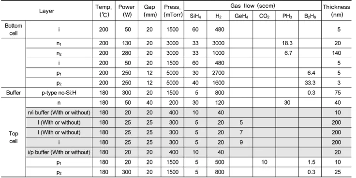
The no.3 showed the Jsc of 22.83 mA/cm2, the Voc of 1.34 V, an FF of 70.22%, and η of 21.47%. The no.4 showed the highest Jsc of 25.22 mA/cm2, the lowest Voc of 1.23 V, an FF of 69.24%, and η of 21.56%. In addition to Figs. 2 and 3 showed optimized thickness of the absorption materials (except no.4- the results depending on thickness were meaningless) for top sub-cell on 2 terminal Si-based tandem junction solar cells by ASA Table 2. Classification of the 2 terminal Si-based tandem
junction solar cells depending on the absorption material of top sub-cell and briefly results by ASA simulation
2 Terminal tandem junction solar cell
No. Classification Top (i) Bottom
1
Materials
a-Si:H (Eg:1.81 eV)
c-Si (1.1 eV)
2 a-SiGe:H
(Eg:1.65 eV)
3 a-SiGe:H
(Eg:1.45 eV)
4 μc-Si:H
(Eg:1.1 eV)
Table 3. Solar cell device parameters of 2 terminal Si-based tandem junction solar cells by ASA simulation No. Jsc (mA/cm2) Voc (V) FF (%) η (%)
1 16.06 1.657 79.66 21.19
2 20.63 1.486 78.72 24.14
3 22.83 1.340 70.22 21.47
4 25.22 1.235 69.24 21.56
30 60 90 120 150 180 210 240 270 300 1.60
1.6578818487 1214 1618 1618 2022
Voc (mV)
Thickness of absorption layer (nm) FF (%)Jsc(mA/cm2 ) (%)
Fig. 2. The optimized thickness of the a-Si:H (1.81 eV) for top sub-cell on 2 terminal c-Si-based tandem junction solar cells by ASA simulation
25 50 75 100 125 150 175 200 225 250 275 300 325 1620
24 1.31.4 1.51.6 7280 88 1620 24
Thickness of absorption layer (nm) Jsc(mA/cm2 )
a-SiGe:H (1.45eV) a-SiGe:H (1.65eV)
Voc(mV)FF (%) (%)
Fig. 3. The optimized thickness of the a-SiGe:H (1.65 eV and 1.45 eV) for top sub-cell on 2 terminal Si-based tandem junction solar cells by ASA simulation
simulation. With increased thickness of absorption layer of solar cells, the Jsc was increased and the FF was dropped. Fig. 2 indicated a-Si:H (1.81 eV) of the 300 nm thick for top sub-cell was appropriated which showed a Jsc of 16.06 mA/cm2, a Voc of 1.657 V, an FF of 79.66%, and η of 21.19%.
Fig. 3 explained a-SiGe:H (1.65 eV) of the 300 nm thick for top sub-cell was appropriated which showed the Jsc of 20.63 mA/cm2, the Voc of 1.48 V, an FF of 78.72%, and η of 24.14%.
And Fig. 3 explained a-SiGe:H (1.45 eV) of the 150 nm thick for top sub-cell was appropriated which showed the Jsc of 22.83 mA/cm2, the Voc of 1.34 V, an FF of 70.22%, and η of 21.47%.
3.2 Optimization of Si-Ge absorption layer of top cell for applying 2 terminal tandem junction solar cells
3.2.1 Optical bandgap engineering depending on germanium ratio
The carriers were generated in the intrinsic (i) layer of amorphous silicon thin film solar cells and it affected the electrical and optical properties. The property of i-layer was related to the Jsc and FF. The a-SiGe:H was used as the i-layer.
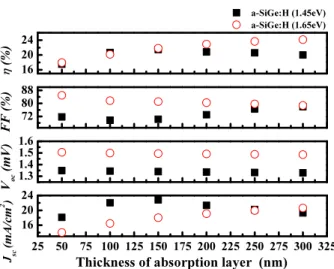
The dependence of bandgap on the germanium (Ge) gas ratio was studied. Figs. 4 and 5 showed that as the Ge gas injection ratio increased from 0% to 50%, the optical band gap dropped from 1.84 V to 1.24 V.
The quantum efficiency of actually fabricated amorphous silicon germanium thin film solar cell was shown in Fig. 6. It could be seen that the optical band gap decreased as the Ge gas ratio was increased and the peak shifts from 520 nm to 590 nm increasing the generation of carriers above 900 nm wavelength.
3.2.2 Optimization of graded buffer (n/i and i/p) layer 3.2.2.1 Optimization of Eg for n/i and i/p buffer layer The drawbacks of reported a-SiGe solar cells were low FF and Voc12) Using ASA simulator, the FF and Voc were improved by optimizing n/i and i/p buffer layers. First, optimum band gap of n/i and i/p buffer layers were simulated. The simulation conditions of optimizing the buffer layers were listed in Table 4.
Fig. 7 showed the structure for the simulation. The thickness of buffer layer is fixed at 10 nm and the band gap was varied from
0.5 1.0 1.5 2.0 2.5 3.0
0 500 1000
1500 Ge percent(%) 0%
10% 20%
30% 40%
2 (ahv) 50%
Photon energy (eV)
Fig. 4. Tauc’s plot of a-SiGe:H depending on Ge ratio Fig. 5. Eg of a-SiGe:H depending on Ge ratio
300 400 500 600 700 800 900 1000
0 10 20 30 40 50 60
70 a-SiGe_0%
a-SiGe_5%
a-SiGe_10%
a-SiGe_15%
Wavelength (nm)
Quantum efficiency (%)
Fig. 6. Quantum efficiency of thin film a-Si solar cells with different Ge ratio in a-SiGe:H absorber layer
Table 4. Conditions of thin film silicon solar cell for optimizing results
Layer Thickness (nm) Ea (eV) Eg (eV)
TCO (FTO) 800 - -
p-a-Si:H (0.05%) 5 0.51 1.81
p-a-SiOx:H (0.25%) 10 0.53 2.05
p/i buffer 10 - Variable
i-a-SiGe (10%) 200 - 1.65
i/n buffer 10 - Variable
n-a-Si:H (1%) 25 0.2 1.81
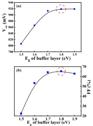
1.5 eV to 1.9 eV. Fig. 8 showed that FF and Voc are better than those without buffer layers when the band gap was more than
1.68 eV but they decrease noticeably when the band gap was lower than 1.68 eV. This could be explained by the band diagram of Fig. 9. When buffer layers were used, the potential barrier of holes at the valence band i/p interface decreased and the conduction band was raised increasing the FF and Voc. Fig.
10 showed I-V properties of solar cells with and without n/i and i/p buffer layer (Eg variation) obtained by ASA simulator. Table 5 showed that the optimum band gap of n/i and i/p buffer layers is 1.8 eV.
3.2.2.2 Optimization of thicknessfor n/i and i/p buffer layer The optimum bandgap was found to be 1.8 eV when the thickness of n/i and i/p buffer layers was 10 nm. These cases, the band gap was fixed at 1.8 eV and the thickness was varied from 4 nm to 12 nm.
The band diagram in Fig. 11 showed that as it got thicker, potential barrier of holes at valance band was decreased and the conduction band was slightly increased resulting in increased FF and Voc. Table 6 presents parameters of thin film solar cells with n/i and i/p buffer layer with different thickness of the buffer layer. It could be concluded that the best solar cell efficiency was obtained when the thickness of buffer layers Fig. 7. Band diagram of thin film silicon solar cell with n/i and i/p
buffer layers
1.5 1.6 1.7 1.8 1.9
780 800 820 840 860 880 900 920 940
Voc (mV)
Eg of buffer layer (eV) (a)
1.5 1.6 1.7 1.8 1.9 20
30 40 50 60 70
FF (%)
Eg of buffer layer (eV) (b)
Fig. 8. (a) The Voc, and (b) FF parameters of thin film silicon solar cell with different Eg of n/i and p/i buffer layers
50 40 30 20 10 0
-1.8 -1.5 -1.2 -0.9 -0.6 -0.30.00.3 0.6 0.9 1.2 1.5
Potential Energy (eV)
Position (nm)
without buffer n/i & i/p buffer (1.8eV) i/p interface
Fig. 9. Band diagrams of thin film solar cells with and without n/i and i/p buffer layers
0.0 0.2 0.4 0.6 0.8
0 2 4 6 8 10 12 14
Current density (mA/cm2 )
Voltage (V) No Buffer
n/i(1.9)_i/p(1.9) n/i(1.8)_i/p(1.8) n/i(1.7)_i/p(1.7) n/i(1.6)_i/p(1.6)
Fig. 10. I-V curves of solar cells with and without n/i and i/p buffer layer (Eg variation) obtained by ASA simulator
Table 5. Photovoltaic parameters of thin film silicon solar cells with n/i and i/p buffer layers with different Eg
SET Voc
(mV) Jsc
(mA/cm2) FF
(%) Eff.
(%)
No buffer 902 13.7 62.90 7.78
n/i (1.9)_i/p (1.9) 919 13.6 62.94 7.88
n/i (1.8)_i/p (1.8) 919 13.6 65.42 8.20
n/i (1.7)_i/p (1.7) 919 13.5 64.33 7.95
n/i (1.6)_i/p (1.6) 866 13.2 53.37 6.12
n/i (1.5)_i/p (1.5) 806 9.43 22.42 1.70
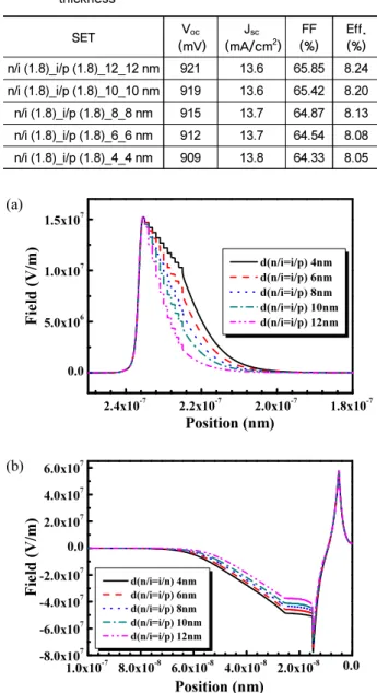
was 10-12 nm. Fig. 12 showed the as the thickness of buffer layer gets thinner than 10 nm, the field got stronger and the collection of carriers increased resulting in increased Jsc.
3.3 Fabrication of 2 terminals thin film Si-Ge/c-Si tandem junction solar cells
The 2 terminals c-Si based tandem junction solar cells were fabricated based on the optimized simulation results (3.1 and 3.2) of the 2 terminals c-Si-based tandem junction solar cells and the thin film a-SiGe:H grading structure for top sub-cell. The I-V characteristics curve and external quantum efficiency of the 2 terminal Si based tandem junction solar cells with different type of absorption layer showed in Fig. 13 and Table 7.
0 200 400 600 800 1000120014001600 0
2 4 6 8 10 12 14
Voltage (mV) Current density (mA/cm2 )
# Tandem cell (1) # Tandem cell (2) # Tandem cell (3) (a)
300 400 500 600 700 800 900 10001100 100
2030 4050 60 7080 90
Wavelength (nm)
Quantum efficiency (%) Tandem cell (1)
Tandem cell (2) Tandem cell (3) (b)
Fig. 13. (a) I-V characteristics curve measured at room tem- perature under AM 1.5 G condition, and (b) external quantum efficiency of the 2 terminal Si based tandem junction solar cells with different type of absorption layer
Table 7. Solar cell parameters calculated by I-V characteristics curve of 2 terminal Si based tandem junction solar cell with different absorption layer
No. Voc
(V) Jsc
(mA/cm2) FF
(%) Eff.
(%)
1 1.44 12.26 67.01 11.84
2 1.44 13.26 66.07 12.62
3 1.48 12.53 70.71 13.11
40 35 30 25 20 15 10 5 0
-1.5 -1.2 -0.9 -0.6 -0.3 0.0 0.3 0.6 0.9 1.2 1.5
d(n/i=i/p) 12nm d(n/i=i/p) 10nm d(n/i=i/p) 8nm d(n/i=i/p) 6nm d(n/i=i/p) 4nm
Potential Energy (eV)
Position (nm)
4 ~ 12 nm
Fig. 11. Band diagrams of thin film solar cells with different thickness of n/i and i/p buffer layer
Table 6. Photovoltaic parameters of thin film silicon solar cells with n/i and i/p buffer layers with different buffer layer thickness
SET Voc
(mV) Jsc
(mA/cm2) FF (%)
Eff.
(%) n/i (1.8)_i/p (1.8)_12_12 nm 921 13.6 65.85 8.24 n/i (1.8)_i/p (1.8)_10_10 nm 919 13.6 65.42 8.20 n/i (1.8)_i/p (1.8)_8_8 nm 915 13.7 64.87 8.13 n/i (1.8)_i/p (1.8)_6_6 nm 912 13.7 64.54 8.08 n/i (1.8)_i/p (1.8)_4_4 nm 909 13.8 64.33 8.05
(a)
2.4x10⁻⁷ 2.2x10⁻⁷ 2.0x10⁻⁷ 1.8x10⁻⁷ 0.0
5.0x10⁶ 1.0x10⁷ 1.5x10⁷
Field (V/m)
Position (nm)
d(n/i=i/p) 4nm d(n/i=i/p) 6nm d(n/i=i/p) 8nm d(n/i=i/p) 10nm d(n/i=i/p) 12nm
(b)
1.0x10⁻⁷ 8.0x10⁻⁸ 6.0x10⁻⁸ 4.0x10⁻⁸ 2.0x10⁻⁸ 0.0 -8.0x10⁷
-6.0x10⁷ -4.0x10⁷ -2.0x10⁷ 0.0 2.0x10⁷ 4.0x10⁷ 6.0x10⁷
Field (V/m)
Position (nm)
d(n/i=i/n) 4nm d(n/i=i/p) 6nm d(n/i=i/p) 8nm d(n/i=i/p) 10nm d(n/i=i/p) 12nm
Fig. 12. Electric fields at (a) n/i or (b) i/p interface on thin film SiGe solar cell
A 75 nm thick p-type nc-Si:H inter layer used for tunneling junction layer on all 2terminal Si based tandem junction solar cells based on previously results13). At first variation of the absorption layer for top sub-cell was carried out with the fixed other layers. a a-SiGe:H with 1.55 eV of Eg applied to absorption layer of top sub-cell for the higher Jsc. The draw backs of reported a-SiGe:H were low FF and Voc. For the high η, the optimization of the buffer layer such as n/i and i/p and the bandgap configuration of absorption layer for the top a-SiGe:H sub-cells were needed. Concentrate, type 1) 600 nm thick Si-Ge with 1.55 eV of Eg – type of the constant Ge concentration, type 2) 600 nm thick a-SiGe:H with a 10 nm thick a-Si:H (1.8 eV of Eg) at n/i and i/p interface, type 3) 200 nm thick a-SiGe:H with 1.65 eV of Eg/200 nm thick a-SiGe:H with 1.60 eV of Eg/200 nm thick a-SiGe:H with 1.55 eV of Eg - gradually increased profile of Ge composition in the direction of the n-type layer were tried to fabricate on the absorption layer of top sub-cell.
Type 1 displayed a Voc of 1.44 V, a Jsc of 12.26 mA/cm2, an FF of 67.01%, and an η of 11.84%. When the n/i and i/p buffer layers were used, the potential barrier of holes at the valence band i/p interface decreases and the conduction band was raised increasing the FF and Voc in theoretically. However, the type 2 was not changed on the Voc and FF. The improved Jsc and spectral response results in Fig. 13 showed that might be buffer layers did not work for reliving discontinued band which played a role in reduced high defect density at the n/i and i/p interfaces14,15) and then lessened recombination of carriers16,17). The type 3 was absorption a-SiGe:H layer with gradually increased profile of Ge composition in the direction of the n-type layer. Type 3 was found that the best FF and Voc was obtained with the thickness of increasing band gap in a-SiGe:H layer and i/p buffer layer was inserted in this structure to increase Jsc. The movement of carriers might get easier improving FF and Voc in graded a-SiGe:H layer. As a result, Voc
of 1.48 V, Jsc of 12.53 mA/cm2, FF of 70.71% and efficiency of 13.11% were obtained which was very promising. The present approach to optimize the bandgap profile by grading Ge composition was thus expected to be very useful to obtain highly efficient 2 terminal thin film Si-Ge/c-Si tandem junction solar cells.
4. Conclusions
For high efficiency of 2 terminals c-Si based tandem junction solar cells, structures of top cell were optimized. First, the
optimal structural results were obtained with the ASA simulator. As a result, it was possible to secure a higher current density and FF when the band gap became narrower and the buffer layer was inserted at the interface before and after the a-SiGe:H absorption layer. The role of the buffer layer was attributed to significantly diminish the band-offset between high band gap p-layer and narrow-gap intrinsic a-SiGe:H layer.
With optimized top cell structure, the thin film SiGe/c-Si tandem junction solar cells are supposed to further improve the Voc, 1.48 V and as a result the performance, 13.11% of the 2 terminals tandem junction configuration solar cells.
Acknowledgments
This works was supported by the research grant of Cheongju University (2019.03.01.~2021.02.28.).
References
1. Loper, P., Niesen, B., Moon, S.J., De Nicolas, S.M., Holovsky, J., Remes, Z., Ledinsky, M., Haug, F.J., Yum, J.H., De Wolf, S., Ballif, C., “Organic–inorganic halide perovskites: Perspectives for silicon-based tandem solar cells,” IEEE J. Photovoltaics, Vol. 4, No. 6, pp. 1545-1551, 2014.
2. Sameshima, T., Takenezawa, J., Hasumi, M., Koida, T., Kaneko, T., Karasawa, M., Kondo, M., “Multi junction solar cells stacked with transparent and conductive adhesive,” Jpn. J.
Appl. Phys., Vol. 50, No. 5R, 052301, 2011.
3. Janz, S., Schnabel, M., LÖper, P., Summonte, C., Canino, M., LÓpez-Vidrier, J., Hernández, S., Garrido, B., Glunz, W.W.,
“Processing and characterisation of tandem solar cells from crystalline silicon materials,” 28th European PV Solar Energy Conference and Exhibition, Paris, France, 2013.
4. Umeno, M., Soga, T., Baskar, K., Jimbo, T., “Hetero epitaxial technologies on Si for high-efficiency solar cells,” Sol. Energy Mater. Sol. Cells, Vol. 50, No. 1-4, pp. 203-212, 1998.
5. Tanabe, K., Watanabe, K., Arakawa, Y., “III-V/Si hybrid photonic devices by direct fusion bonding,” Nat. Sci. Rep., Vol.
2, 349, 2012.
6. Beiley, Z.M., McGehee, M.D., “Modeling low cost hybrid tandem photovoltaics with the potential for efficiencies exceeding 20%,” Energy Environ. Sci., Vol. 5, pp. 9173-9179, 2012.
7. Bailie, C.D., Christoforo, M.G., Mailoa, J.P., Bowring, A.R., Unger, E.L., Nguyen, W.H., Burschka, J., Pellet, N., Lee, J.Z., Grätzel, M., Noufi, R., Buonassisi, T., Salleo, A., McGehee, M.D., “Semi-transparent perovskite solar cells for tandems with silicon and CIGS,” Energy Environ. Sci., Vol. 8, pp.
956-963, 2015.
8. Blocker, W., “High-efficiency solar energy conversion through
flux concentration and spectrum splitting,” Proc. IEEE, Vol. 66 pp. 104-105, 1978.
9. Kim, S., Kasashima, S., Sichanugrist, P., Kobayashi, T., Nakada, T., Konagai, M., “Development of thin-film solar cells using solar spectrum splitting technique,” Sol. Energy Mater.
Sol. Cells, Vol. 119, pp. 214-218, 2013.
10. Wang, X., Waite, N., Murcia, P., Emery, K., Steiner, M., Kiamilev, F., Goossen, K., Honsberg, C., Barnett, A., “Lateral spectrum splitting concentrator photovoltaics: direct measurement of component and submodule efficiency,” Prog. Photovoltaics Res. Appl., Vol. 20, pp. 149-165, 2012.
11. Yan, J., Thomas, F., Romain, C., Galo, T. S., Thierry, M., Stefano, P., Rolf, E., Marta, D.R., Mario, O., Ramis, H., Ayodhya, N.T., and Fan, F., “High-mobility In2O3:H electrodes for four-terminal perovskite/CuInSe2 tandem solar cells,” ACS Nano, Vol. 14, No. 6, pp. 7502–7512, 2020.
12. Lundszien, D., Finger, F., and Wagner, H., “A-Si:H buffer in a-SiGe:H solar cells,” Solar Energy Materials & Solar Cells, Vol. 74, pp. 365–372, 2002.
13. Park, J., Kim, S., Phong, P. D., Lee, S., Yi, J., “Improved carrier tunneling and recombination in tandem solar cell with p-type nanocrystalline Si intermediate layer,” Current Photo- voltaic Research, Vol. 8, No. 1, pp. 6-11, 2020.
14. Lundszien, D., Finger, F., Wagner, H., “Band-gap profiling in amorphous silicon–germanium solar cells,” Appl. Phys. Lett., Vol. 80, 1655, 2002.
15. Arya, R.R., Catalano, A., Oswald, R.S., “Amorphous silicon p
‐i‐n solar cells with graded interface,” Appl. Phys. Lett., Vol. 49, 1089, 1986.
16. Zimmer, J., Stiebig, H., Wagner, H., “a-SiGe:H based solar cells with graded absorption layer,” J. Appl. Phys., Vol. 84, 611, 1998.
17. Fan, Q. H., Chen, C., Liao, X., Xiang, X., Zhang, S., Ingler, W., Adiga, N., Hub, Z., Cao, X., Du, W., Deng, X., “High efficiency silicon–germanium thin film solar cells using graded absorber layer,” Sol. Energy Mater. Sol. Cells, Vol. 94, 1300, 2010.