반도체디스플레이기술학회지 제16권 제1호(2017년 3월) Journal of the Semiconductor & Display Technology, Vol. 16, No. 1. March 2017.
TCAD Simulation of Silicon Pillar Array Solar Cells
Hoong Joo Lee
*†*†
Department of Electronic Engineering, Sangmyung University
ABSTRACT
This paper presents a Technology-CAD (TCAD) simulation of the characteristics of crystalline Si pillar array solar cells. The junction depth and the surface concentration of the solar cells were optimized to obtain the targeted sheet resistance of the emitter region. The diffusion model was determined by calibrating the emitter doping profile of the microscale silicon pillars. The dimension parameters determining the pillar shape, such as width, height, and spacing were varied within a simulation window from ~2μm to 5μm. The simulation showed that increasing pillar width (or diameter) and spacing resulted in the decrease of current density due to surface area loss, light trapping loss, and high reflectance. Although increasing pillar height might improve the chances of light trapping, the recombination loss due to the increase in the carrier’s transfer length canceled out the positive effect to the photo-generation component of the current. The silicon pillars were experimentally formed by photoresist patterning and electroless etching. The laboratory results of a fabricated Si pillar solar cell showed the efficiency and the fill factor to be close to the simulation results.
Key Words : Solar Cell, TCAD
1. Introduction
1
Silicon micropillar or nanowire arrays with high aspect ratio and radial p-n junctions could be a promising structure for low-cost and high-efficiency solar cells [1].
Micropillar or nanowire arrays have been of interest due to the enhanced light trapping inherent to pillar geometry and high carrier collection efficiency [2]. Several different types of pillar arrays used to fabricate Si solar cells have been reported using various processing methods such as chemically grown Si nanowires [3,4], reactive ion etched Si micropillars [1,5,6], and Si micropillars with chemical etching [2,7]. Even though the radial p-n junction of the microwire array decouples the increased light absorption and carrier collection paths and shortens the carrier conduction paths, the performance of the array typed Si solar cells previously reported has not been superior to that of the planar cells because the increased surface
†
E-mail: [email protected]
recombination of the carriers in the enlarged surface area could limit the overall efficiency [2,5,7]. TCAD simulation study is needed to understand the inherent physical, and geometry dependent device properties of wire array solar cells, and to optimize light absorption and carrier collection efficiency [8]. In this paper, the simulation studies based on process and device simulation, of the effect on the dimensions determining the pillar shape, such as width (or diameter), height, and spacing are presented. A proper, calibrated two- dimensional diffusion model is discussed to study the effect of emitter junction depth and surface doping concentration of the pillars. An experiment has been done using a cell performance measurement with successive semiconductor processing steps to compare the simulation results of the Si pillar solar cell to those of the fabricated one.
2. Experiment
A 720µm thick polished silicon substrate with (100)
Hoong Joo Lee 66
orientation was prepared to fabricate the micropillar solar cells. It was a p-type doped wafer with a resistivity of 8~12Ωcm. The Si pillar arrays were fabricated using metal-induced electroless etching [9]. Ag particles were first precipitated onto a hydrogen terminated Si wafer by electroless deposition in an aqueous solution of 4.8M hydrofluoric acid (HF) and 10mM AgNO
3at room temperature. After the deposition of the metal particles, the sample wafer was immersed in an oxidizing HF etching solution with 4.8M HF acid and 0.5M H
2O
2, then rinsed with deionized water and dried at room temperature. The electroless etching step resulted in the formation of vertically aligned and cointegrated arrays including both Si nanopillars and micropillars. Ag particles remaining after completion of electroless etching were dissolved in dilute nitric acid (HNO
3), and then the samples were cleaned in acetone to remove all photoresist remaining on top of the micropillars. Further chemical etching using a 10 wt% aqueous KOH solution was performed to remove the nanopillars leaving the micropillars. The total etching time to form the micropillars depends on the targeted aspect ratio and the spacing of the pillars [10]. POCl
3doping was then performed to form the n
+emitter region.
200sccm of POCl
3flow was introduced into the furnace under O
2ambient during deposition and drive-in steps.
After PSG removal by HF dip, Al paste was screen-printed on the backside and dried. Ag grid was then screen-printed on the emitter and dried. Ag and Al layers were co-fired in the furnace to form ohmic contacts to n
+emitters and Al back surface fields (BSF). The light-current-voltage (LIV) characteristics of the Si pillar solar cells were investigated under air mass 1.5G (1000mW/cm
2) illumination with a solar simulator.
TCAD simulation was performed using a Silvaco process and device simulator which calculates optical generation rate with a ray tracing model and solves Poisson’s and continuity equations. Secondary Ion Mass Spectrometry (SIMS) measurements were also performed to obtain the doping profiles inside the Si pillars.
3. Results and Discussion
Fig.1 shows the simulation structure of Si micropillar solar cells, which have radial p-n junctions. The simulation windows for the geometry are from 1.5μm to 5μm for the
pillar width, and 2μm to 5μm for both the pillar height and the spacing. To determine a diffusion model for the n
+emitter, calibration for the emitter doping profile was done using the fabricated pillar. The fabricated pillar had a width of 2μm, a height of 4μm, and a spacing of 4μm.
Fig. 1. Simulation structure of micropillar Si solar cells.
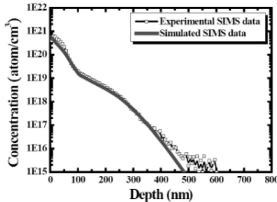
Fig. 2. Emitter doping profile and the calibrated simulation profile with a combined doping model.
As shown in Fig. 2, using a fully coupled diffusion
model the simulation profile can be fitted best to the SIMS
graph. The diffusion model describes well the defect-
dopant pair diffusion mechanism along with point defect
generation during the phosphorus predeposition and drive-
in for the POCl
3doping. The simulation shows a kink near
the surface region and a tail behavior comparable to the
experimental result. At large depths, the two profiles differ,
because in SIMS, the phosphorus density may be
overestimated due to ion mixing, ion segregation and
surface roughness associated with the relatively high-
energy ion beam [11].
TCAD Simulation of Silicon Pillar Array Solar Cells 67
Fig. 3. Emitter doping simulation in case of surface concentration of 5x10
19cm
-3and 5x10
20cm
-3to get the targeted sheet resistance and the junction depth.
After the emitter diffusion profile calibration, the effect of sheet resistance (R
S) of the emitter region and the junction depth (Xj) to the solar cell performance has been investigated according to the different values of surface concentration (N
S). Fig. 3 shows the emitter doping process simulation for the targeted sheet resistance and the junction depth, which are fed back to the device simulation to evaluate the solar cell device characteristics such as efficiency (η) and fill factor (FF). As N
Sgets higher, Xj becomes shallower to get the same R
S. The proper values for N
Sshould also be selected to maintain the formation of the radial p-n junction inside the pillar.
Fig. 4 shows external quantum efficiency of Si micropillars for the different emitter R
Svalues. As Xj of the emitter gets shallower, the lower recombination rate causes the quantum efficiency to be higher at the short wavelengths, increasing the current density (J
SC). However, the shallower Xj might lead to higher series resistance of the emitter, causing the reduced FF. The η increases with the increased R
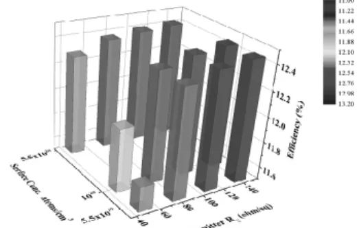
Sof the emitter. The efficiency (η) simulation results as shown in Fig. 5 show the highest value of ~12% with R
Sat the level of 140Ω/sq for a cell
dimension with a width of 2μm, a height of 4μm, and a spacing of 4μm.
Fig. 4. External quantum efficiency of Si micropillars with the different emitter sheet resistance values.
Fig. 5. Efficiency simulation with the emitter sheet resistance and the surface concentration for the Si pillar solar cell with a width of 2μm, a height of 4μm, and a spacing of 4μm.
Fig. 6. LIV curve Comparison between simulation and experiment for Si pillar solar cell.
It is shown in Fig. 6 that a LIV (light-current-voltage)
curve with J
SCand an open circuit voltage (V
OC) predicted
Hoong Joo Lee 68
by the simulation is quite similar to the measured performance of the fabricated cell. The density (D) is the ratio of the top area occupied with the pillars to the planar wafer area. Fig. 7 shows the J
SCvariation based on the density of the pillars on the silicon surface with a fixed height of 2μm. J
SCincreases with D, meaning that light is more absorbed into the denser structure of the pillars, generating more photo-carriers. The higher J
SCcan be expected with the same pillar density when the pillar width becomes thinner, due to the increased vertical surface area which absorbs more incident and reflected light. However, the increased D can lower V
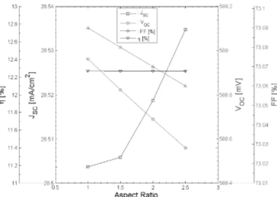
OCand FF due to the enhanced recombination at the increased junction and the pillar surface. Fig. 8 shows J
SC, V
OC, FF, and η simulation results depending on the aspect ratio (AR) of the pillar for the case of the width of 4μm and the spacing of 2μm. The aspect ratio is defined as a ratio of the pillar height to the pillar width. Pillars fabricated with a longer wet etching time will be taller and have an increased AR. J
SCcontinues to increase with higher AR because the light trapping path length inside the space between neighboring pillars increases with the depth of the space, namely, the pillar height. The leakage current due to the recombination at the increased surface of the longer pillar can, however, offset the favorable gain of J
SC. The trend of decreasing V
OCand FF also represents the recombination and the higher series resistance which the photo-generated carriers suffer from in traveling along the longer path to the contacts. Thus, the efficiency η of the pillar solar cells is shown to be nearly unchanged, regardless of the pillar geometry.
Fig. 7. J
SCand V
OCsimulation results based on the pillar density with a constant pillar height of 2μm.
Fig. 8. J
SC, V
OC, FF, and η simulation results based on the aspect ratio of the pillar with a constant spacing of 2μm and a width of 4μm.
4. Conclusion and Future Work
TCAD simulation for the silicon pillar solar cells shows that without surface passivation in the fabrication process, the net efficiency of the pillar solar cell might not to be enhanced with the surface increase. Even though the calibration for the emitter junction profile might raise the prediction ability for the cell performance, the defect density at the increased unpassivated surface which is not only depending on the wet etching process but also affecting the recombination current must be considered in the calibration to achieve the more accurate geometry dependence.
References
1. Yoon, H. P., Yuwen ,Y. A., Shen, H., Podraza, N. J., Mallouk, T. E., Dickey, E. C., Redwing, J. A., Wronski, C. R., and Mayer, T. S., “Parametric Study of Micropillar Array Solar Cells,” Proceeding of IEEE 37th Photovoltaic Specialists Conference, pp. 303-306, 2011.
2. Shin, J. C., Chanda, D., Chern, W., Yu, K. J., Rogers, J.
J., and Li, X., “Experimental Study of Design Parameters in Silicon Micropillar Array Solar Cells Produced by Soft Lithography and Metal-Assisted Chemical Etching,” IEEE J. of Photovoltaics, Vol. 2, pp.
129-133, 2012.
3. Park, W. I., Zheng, G., Jiang, X., Tian, B., and Lieber, C.
M., “Controlled Synthesis of Millimeter-long Silicon
Nanowires with Uniform Electronic Properties,” Nano
Letters, Vol. 8, pp. 3004-3009, 2008.
TCAD Simulation of Silicon Pillar Array Solar Cells 69