• 검색 결과가 없습니다.

Characterization of Combined Micro- and Nano-structure Silicon Solar Cells using a POCl3 Doping Process

N/A
N/A
Protected

Academic year: 2021

Share "Characterization of Combined Micro- and Nano-structure Silicon Solar Cells using a POCl3 Doping Process"

Copied!
4
0
0

로드 중.... (전체 텍스트 보기)

전체 글

(1)

1. Introduction

Photovoltaic technology based on crystalline silicon(c-Si) solar cells has been widely developed for high efficiency and reliability. Currently, c-Si solar cells account for about 80% to 90% of photovoltaic market. However, the complicated process of the conventional c-Si technology might be seen as a sign of its limitation to cost-effective and higher efficiency. For this reason, many researcher and scientists have intensively proposed new and novel concepts such as quantum dot

1)

, plasmonic effect

2)

and nano-structure

3)

for overcoming its limitation. Among them, silicon nanostructure have been intensively investigated for their potential use in cost-effective third-generation high efficiency solar cells due to their unique optical and electrical characteristics

4-7)

. There are two big advantages of getting higher efficiency. One is radial p-n junction, which can be theoretically explained that diffused minority carriers are not oppositely but orthogonally separated for reduction of material consumption

8, 9)

. The other is anti-reflection effect due to strong light trapping by multiple scattering of the incident light

10)

.

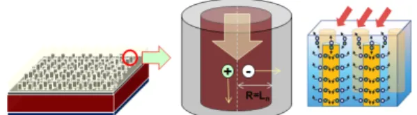
Microwires(MWs) can be contributing to radial p-n junction and nanowires(NWs) to anti-reflection effect. Figure 1 shows schematic illustration of microstructre silicon and radial junction effect due to orthogonal separation in directions. The combined micro and nanowires(CNMWs) silicon solar cells has been particularly suggested for taking all the good points.

Atwater et al

11)

. reported that CNMWs Si solar cells would be expected for achieving 14.5% of conversion efficiency based on simulation results. CNMWs Si solar cells, recently fabricated by J. H. Lee group
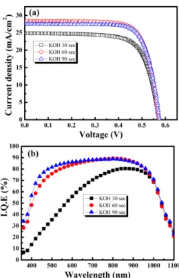
12)

, showed 8.45% of conversion efficiency from spin on doping(SOD) method for emitter process. Several alter- natives to improvement of low efficiency should be suggested from a processing perspective such as emitter process, metalliza- tion and feasibility of transparent conducting oxide (TCO) thin films.

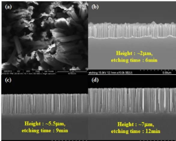
As a first step, we fabricated CNMWs Si solar cells using POCl

3

emitter process after Ag assisted electroless etching

Current Photovoltaic Research 1(1) 69-72 (2013) pISSN 2288-3274

Characterization of Combined Micro ‐ and Nano‐structure Silicon Solar Cells using a POCl 3 Doping Process

Chaehwan Jeong

1)

* ․ Changheon Kim

1, 3)

․ Jonghwan Lee

1)

․ Junsin Yi

2)

․ Sangwoo Lim

3)

․ Suk-Ho Lee

4)

1)

Energy and Applied Optics Research Group, Korea Institute of Industrial Technology, Gwangju 500-480, Korea

2)

Department of Electronic Electronical Engineering, Sungkyunkwan University, Suwon 440-756, Korea

3)

Department of Chemical and Biomolecular Engineering, Yonsei University, Seoul 120-749, Korea

4)

Research and business development team, Southwestern Research Institute of Green Energy Technology, Mokpo 530-400, Korea

ABSTRACT: Combined nano‐ and micro‐wires (CNMWs) Si arrays were prepared using PR patterning and silver‐assisted electroless etching.

A POCl

3

doping process was applied to the fabrication of CNMWs solar cells. KOH solution was used to remove bundles in CNMWs and the etching time was varied from 30 to 240 s. The lowest reflectance of 3.83% was obtained at KOH etching time of 30 s, but the highest carrier lifetime of 354 µs was observed after the doping process at 60 s. At the same etching time, a V

oc

of 574 mV, J

sc

of 28.41 mA/cm

2

, FF of 74.4%, and Eff. of 12.2% were achieved in the CNMWs solar cell. CNMWs solar cells have potential for higher efficiency by improving the post ‐ process and surface ‐rear side structure.

Key words: silicon solar cell, nanowire, microwire, electroless etching

*Corresponding author: [email protected] Received April 8, 2013; Revised April 15, 2013;

Accepted April 18, 2013

ⓒ 2013 by Korea Photovoltaic Society

This is an Open Access article distributed under the terms of the Creative Commons Attribution Non-Commercial License (http://creativecommons.org/licenses/by-nc/3.0)

which permits unrestricted non-commercial use, distribution, and reproduction in any medium, provided the original work is properly cited.

Fig. 1. Schematic illustration of microstructure Si and radial junction effect

69

(2)

C.H. Jeeog et al. / Current Photovoltaic Research 1(1) 69-72 (2013) 70

process and produced simulation results of various parameters as well.

2. Experimental Procedure

2.1 Preparation of NWs and CNMWs

Firstly, silver nanoparticles were uniformly deposited onto unetched PR patterned Si wafer using a mixed solution of deionized water, HF (4.8 M) and AgNO

3

(0.01 M) at 20 ℃ for 1 min. Chemical etching in a mixed solution of deionzed water, HF (4.8 M) and H

2

O

2

(0.5 M) was used to etch a vertically aligned NW Si array with a height range of 2~7 μm. Silver nanoparticles were easily removed using nitric acid after completion of the electroless etching. In order to form CNMWs onto Si wafer, it was prepared by photolithography followed by silver-assisted electroless etching for 6 min. Mask with 2 μm dot and 5 μm gap was used for photoresisit (PR) pattern. Bundles of NWs and CNMWs were observed due to agglomeration at their tops-ends. For the removal of bundles, chemical etching using a 30wt% aqueous potassium hydroxide (KOH) solution at 20℃

was used just after silver-assisted etching in order to decrease the areal density of NWs. KOH etching time was varied from 30 sec to 90 sec. All prepared samples were measured by UV- Vis-NIR spectrometer (Cary 5000, Varian Inc.) and field emission scanning electron microscope (FESEM, JEOL) for investigation of reflectance and cross-sectional views.

2.2 Fabrication of CNMWs Si solar cells

CNMWs solar cells were fabricated with KOH etching time, fixed at 860℃ of doping temperature for 20 min. And then, minority carrier lifetime and sheet resistance of samples were measured by quasi steady state photoconductive (QSSPC, WCT-150, sinton- consulting) and four point probe system (changmin Tech.). LIV and internal quantum efficiency (IQE) of all CNMWs Si solar cells were measured by solar simulator (WXS-1555S-L2, AM 1.5G, Wacom) and spectral response measurement system (CEP-25BX, Jasco).

3. Results and Discussion

3.1 Formation of SiNWs

Figure 2 (a), (b), (c) and (d) show the top and cross-sectional views of SiNWs with variation of etching time. As etching time was increased to 12 min, height of SiNWs was proportionally increased from 2 μm to 7 μm. Also, it was confirmed that

reflectance of SiNWs was proportional to etching time, shown in Fig. 3.

3.2 Formation of CNMWs by KOH etching and their characterization

KOH solution with 10 wt% was used for the removal of bundles at the top of CNMWs because lots of bundles, bringing about incomplete and conformal post-process

12, 13)

, should have a harmful influence on fabrication of high efficient CNMWs solar cells. Figure 4 shows top and cross-sectional views of CNMWs after dipping KOH solution. As KOH etching time was more increased, densities of bundles were more reduced. It is actually sufficient to remove lots of bundles in a short space of time (around 30 sec). When KOH etching time was 90 sec, SiNWs were very much non-existent, supposedly due to excessive etching reaction in the allotted time. Even CNMWs over KOH etching time of 120 sec seemed to be deformed.

Figure 5 shows reflectance of Si bare wafer and CNMWs before and after KOH etching. Average reflectance of Si bare Fig. 2. Top (a) and cross-sectional (b), (c) and (d) views of SiNWs

with increase of etching time

Fig. 3. Reflectance of SiNWs with increase of etching time

(3)

C.H. Jeeog et al. / Current Photovoltaic Research 1(1) 69-72 (2013) 71

wafer was about 37.83% in the wavelength range of 300 ~ 1,200 nm. The lowest average reflectance, corresponded with 3.83%, did not show CNMWs before KOH etching but rather after KOH etching for 30sec. However, their reflectance were more increased to 34.76% after KOH etching time of 60 sec. In order to fabricate CNMWs solar cells with variation of KOH etching time, 30, 60 and 90 sec of KOH etching time could be determined by taking advantage of optical reflectance above explained.

Excessive KOH-etched CNMWs would be of the mark in this study.

3.3 Fabrication of CNMWs solar cells after KOH etching

CNMWs solar cells after KOH etching were fabricated using POCl

3

doping process for formation of emitter region. All samples were doped at 860 ℃ for 20min and average sheet resistance was around 50 Ω/sq. Minority carrier lifetime of CNMWs after KOH etching were measured before POCl

3

doping process. As shown in Fig. 6, They showed severely low carrier lifetime of 10 μs ~ 13 μs despite semiconductor grade Si wafer with high purity.

After POCl

3

doping process, carrier lifetime of CNMWs was

about 30 times more improved to 324 μs ~ 354 μs. When KOH etching time was 60 sec, the best carrier lifetime of 354 μs was obtained. In case of KOH etching time of 30 sec, current terms would be decreased due to high surface recombination rate.

Figure 7 (a) and (b) show LIV and IQE characteristics of CNMWs solar cells after KOH etching process. 12.2% of the highest conversion efficiency in CNMW solar cells was obtained from KOH etching time of 60 sec, corresponded to the best carrier lifetime. Three CNMWs solar cells showed the similar V

oc

value of about 575 mV but, there was a big J

sc

difference between KOH etching time of 30 sec and the others. Also, poor

Fig. 6. Minority carrier lifetime of CNMWs before and after KOH etching

Fig. 7. LIV (a) and IQE (b) characteristics of CNMWs solar cells after KOH etching process

Fig. 4. Top and cross-sectional views of CNMWs after KOH etching time of 30 sec (a), 60 sec (b), 90 sec (c), 120 sec (d) and 240 sec (e)

Fig. 5. Reflectance of Si bare wafer and CNMWs before and

after KOH etching

(4)

C.H. Jeeog et al. / Current Photovoltaic Research 1(1) 69-72 (2013) 72

spectral response and IQE value in the short wavelength range was observed at KOH etching time of 30 sec. Additional pro- cesses such as passivation and gap filling between CNMWs would be significant for improvement of performance in CNMWs solar cells. Light trapping effect was remarkably reduced at KOH etching time of 90 sec, resulting in decrease of J

sc

. As a result, CNMWs solar cells with V

oc

of 574 mV, J

sc

of 28.41 mA/cm

2

, FF of 74.4% and Eff. of 12.2% could be fabricated at KOH etching time of 60 sec.

4. Conclusion

We prepared CNMWs Si array using PR patterning and silver-assisted electroless etching and then, fabricated solar cells using POCl

3

doping process and metallization without anti-reflection layer. Lots of bundles in CNMWs can be easily reduced or removed using KOH etching solution. The optimized KOH etching time was known to be 30 sec ~ 90 sec after confirma- tion by SEM images and reflectance. Within the given conditions, the highest carrier lifetime and LIV characteristics were shown at KOH etching time of 60 sec. Our works suggests that densities of SiNWs should be properly distributed in CNMWs matrix. We achieved the performance of CNMWs with V

oc

of 574 mV, J

sc

of 28.41 mA/cm

2

, FF of 74.4% and Eff. of 12.2%. For reduction of recombination rate in emitter region, sheet resistance would be much higher value of 80 ~ 100 Ω/sq. CNMWs solar cells would have a big potential for achievement of the highest efficiency by optimization of passivation process and improvement of cell structure such as selective emitter structure with increase of current density in the short wavelength region and local back contact process with increase of voltage.

Acknowledgement

This work was supported by the New & Renewable Energy Technology Development Program of the Korea Institute of Energy Technology Evaluation and Planning (KETEP) grant funded by Ministry of Knowledge Economy of the Korean government. (Granted No. : 20113020010010)

References

1. C. W Jiang and M. A. Green, “Silicon quantum dot superlattice : Modeling of energy bands, densities of states, and mobilities for silicon tandem solar cell application”, J. Appl. Phys., Vol.

99, pp. 114902-114902-7, 2006.

2. V. E. Ferry, L. A. Sweatlock, D. Pacifici and H. A. Atwater,

“Plasmonic nanostructure design for efficient light coupling in- to solar cells”, Nano Lett., Vol. 8, pp. 4391-4397, 2008.

3. J. Y. Jung, Z. Guo, S. W. Jee, H. D. Um, K. T. Park and J. H.

Lee, “A strong antireflective solar cell prepared by tapering sili- con nanowires” Opt. Express, Vol. 18, pp. A286-A292, 2010.

4. B. Tian, X. Zheng, T. J. Kempa, Y. Fang, N. Yu, G. Yu, J.

Huang and C. M. Lieber, “Coaxial silicon nanowires as solar cells and nanoelectronic power sources”, Nature, Vol. 449, pp.885-889, 2007.

5. E. C. Garnett and P. D. Yang, “Silicon nanowire radial p-n jun- cition solar cells”, J. Am. Chem. Soc., Vol. 130, pp. 9224-9225, 2008.

6. C. Lin and M. L. Povinelli, “Optical absorption enhancement in silicon nanowire arrays with a large lattice constant for pho- tovoltaic applications”, Opt. Express, Vol. 17, pp. 19371-19381, 2009.

7. Y. M. Song, J. S. Yu and Y. T. Lee, “Antireflective sub- micrometer gratings on thin film silicon solar cells for light-ab- sorption enhancement”, Opt. Lett., Vol. 35, pp. 276-278, 2010.

8. K. Peng, Y. Xu, Y. Wu, Y. Yan, S. T. Lee and J. Zhu, “Aligned single-crsytalline Si nanowire arrays for photovoltaic applica- tions”, Samll, Vol. 1, pp. 1062-1067, 2005.

9. V. Sivakov, G. Andra, A. Gawlik, A. Berger, J. Plentz, F. Falk and S. H. Christiansen, “Silicon nanowire-based solar cells on glass: synthesis, optical properties and cell parameters”, Nano Lett., Vol. 9. pp. 1549-1554, 2009.

10. L. Tsakalakos, J. Balch, J. Fronheiser, M. Y. Shih, SF.

LeBoeuf, M. Piertzykowski, P. J. Codella, B. A. Korevaar, O.

Sulima, J. Rand, A. Davuluru, and U. Rapol, “Strong broad- band optical absorption in silicon nanowire films”, J.

Naophotonics, Vol. 1, pp. 013552, 2007.

11. M. D. Kelzenberg, M. C. Putnam, D. B. Turner-Evans, N. S.

Lewis and H. A. Atwater, “Predeicted efficiency of Si wire ar- ray solar cells”, Proc. of 34th IEEE 001948, 2007.

12. H. D. Um, J. Y. Jung, X. Li, S. W. Jee, K. T. Park, H. S. Seo, S. A. Moiz, S. W. Lee, J. Y. Ji, C. T. Kim, M. S. Hyum, Y. C.

Park, J. M. Yang and J. H. Lee, “A novel photovoltaic nano- device based on the co-integration of silicon micro and nano- wires prepared by electroless etching with conformal plasma doping” Proc. of IEEE, pp. 1, 2009.

13. H. D. Um, J. Y. Jung, H. S. Seo, K. T. Park, S. W. Jee, S. A.

Moiz and J. H. Lee, “Silicon nanowire array solar cell prepared

by metal-induced electroless etching with a novel processing

technology”, Jpn. J. Appl. Phys., Vol. 49, pp. 1-5, 2010.

수치

Fig. 1. Schematic illustration of microstructure Si and radial  junction effect
Figure 2 (a), (b), (c) and (d) show the top and cross-sectional  views of SiNWs with variation of etching time
Fig. 6. Minority carrier lifetime of CNMWs before and after KOH  etching

참조

관련 문서

Using a combined CVD and ALD equipment system, multi-layer quantum well structures of Al 2 O 3 /a-Si/Al 2 O 3 were fabricated on silicon Schottky junction devices and implemented