[논 문] 한국재료학회지 http://dx.doi.org/10.3740/MRSK.2012.22.9.450 Kor. J. Mater. Res.
Vol. 22, No. 9 (2012)
450
†Corresponding author
E-Mail : [email protected] (K. S. Choe)
Simulated Optimum Substrate Thicknesses for the BC-BJ Si and GaAs Solar Cells
Kwang Su Choe
†Dept. of Electronic Materials Engineering, College of Engineering, The University of Suwon, Hwaseong-Shi, Gyeonggi-Do 445-743, Korea
(Received June 25, 2012 : Received in revised form July 31, 2012 : Accepted August 1, 2012)
Abstract
In crystalline solar cells, the substrate itself constitutes a large portion of the fabrication cost as it is derived from semiconductor ingots grown in costly high temperature processes. Thinner wafer substrates allow some cost saving as more wafers can be sliced from a given ingot, although technological limitations in slicing or sawing of wafers off an ingot, as well as the physical strength of the sliced wafers, put a lower limit on the substrate thickness. Complementary to these economical and techno-physical points of view, a device operation point of view of the substrate thickness would be useful. With this in mind, BC-BJ Si and GaAs solar cells are compared one to one by means of the Medici device simulation, with a particular emphasis on the substrate thickness. Under ideal conditions of 0.6µm photons entering the 10 µm-wide BC-BJ solar cells at the normal incident angle (θ = 90o), GaAs is about 2.3 times more efficient than Si in terms of peak cell power output:42.3 mW·cm−2 vs. 18.2 mW·cm−2. This strong performance of GaAs, though only under ideal conditions, gives a strong indication that this material could stand competitively against Si, despite its known high material and process costs. Within the limitation of the minority carrier recombination lifetime value of 5× 10⁻⁵ sec used in the device simulation, the solar cell power is known to be only weakly dependent on the substrate thickness, particularly under about 100µm, for both Si and GaAs.
Though the optimum substrate thickness is about 100µm or less, the reduction in the power output is less than 10% from the peak values even when the substrate thickness is increased to 190µm. Thus, for crystalline Si and GaAs with a relatively long recombination lifetime, extra efforts to be spent on thinning the substrate should be weighed against the expected actual gain in the solar cell output power.
Key words
solar cell simulation, Si solar cell, GaAs solar cell, BC-BJ solar cell, Medici.1. Introduction
Despite the efforts and progresses over the past 50 years, the solar cell energy is still too expensive, even at the current energy conversion efficiency or PCE (Photon- to-Current Efficiency) of about 20%, or 20 mW·cm
−2under AM1.5.
1)Currently, the solar energy, at about 50 cents per kWh, is at least 5 times more expensive than the coal, oil, nuclear and even wind energy.
2)Nonetheless, as the energy arriving on the earth surface from the sun in the form of light is approximately 10,000 times the total energy consumed by the whole of the humanity, the solar cell technology is possibly the only one that can promise to serve our energy needs indefinitely into the future.
Of the known types of the solar cells, the crystalline silicon solar cell still accounts for nearly 95% of the global production.
2)This is in part due to the ready availability of the silicon material, the second most abundant element on earth, and the relatively high energy conversion efficiencies,
which are known to approach 22% and 17% for device and module, respectively, in production. The thermal budget for fabricating a crystalline solar cell is extremely high, as the process temperature for growing or casting silicon ingots is as high as 1500
oC and that for forming the pn junction as high as 1000
oC. As such, there is a lower limit as to how much the production cost can be reduced to. The thermal budget and the production cost are even higher for the GaAs-based solar cells. This is because GaAs is extremely difficult material to grow or cast in ingot form and to work with in thermal processes. Less costly solar cells in the form of semiconductor thin films, dye-sensitized inorganic particles, organic thin films and others have been developed and mass-produced. However, these all suffer from low energy conversion efficiency to some extent as the efficiency is invariably related to the cost.
While the theoretical limit of the energy conversion effi-
ciency for the Si solar cell is known to be less than
30%,
3)the highest efficiency reported for an actual cell is
24.7% by the PERL (Passivated Emitter, Rear Locally-
diffused) method.
4)As for the GaAs-based solar cells, the
Simulated Optimum Substrate Thicknesses for the BC-BJ Si and GaAs Solar Cells 451
theoretical and practical limits of the efficiency are much higher. It is generally believed that the theoretical limit of the solar cell efficiency for GaAs is about 30% higher than that of Si in relative term. In practice, an efficiency of nearly 60% was achieved in multi-junction GaAs- based solar cells fabricated monolithically on a single substrate using tunnel junction connections.
5)The BC-BJ (Back-Contact Back-Junction) design, also known as back-lit design, is lately gaining wider accep- tance mainly due to some intrinsic benefits. That is, by placing both the emitter and base electrodes on one side, the electrical shading is eliminated, the surface can be better passivated, the series connections between the cells are hidden, and the surface is visually more appealing.
With better-quality substrate materials, these intrinsic benefits could outweigh the loss due to the increased carrier recombination in the bulk.
For slow-absorbing indirect-gap semiconductors like Si, the back-lit design is more appealing because the photons must penetrate deeper before being completely absorbed. In Si, it is estimated that the distance is about 100 µm for 90% of the incident photons are to be absorbed. For the fast-absorbing direct-gap semiconductors like GaAs, the back-lit design may be less appealing.
Thus, one-to-one comparison between the two types of the material should be of value in itself.
In terms of the solar cell fabrication cost, the substrate itself constitutes a large portion as it is derived from semi- conductor ingots grown in costly high temperature pro- cesses. Some cost saving, therefore, can be achieved by slicing more wafers out of a given ingot, resulting in thinner wafer substrates. At the same time, the technological limitations in slicing or sawing the wafers off an ingot as well as the physical strength of the sliced wafers put a lower limit on the substrate thickness. In this regard, an independent study on the optimum substrate thickness from the device operation point of view would complement the aforementioned economical and technological points of view and aid in determining the realistic substrate thick- nesses for Si and GaAs solar cells.
In this work, with emphasis on the BC-BJ design, the solar cell operation, particularly in terms of the power output, is closely examined as a function of the substrate thickness by employing the Medici device simulator. The result of the study should indicate the optimum substrate thickness values for the BC-BJ solar cell design.
2. Experimental Procedure
The method and approach used in this simulation ex- periment are similar to those outlined in the earlier published work dealing exclusively with the BC-BJ Si solar cell.
6)The generic device simulation consists of four
major steps: grid formation, model and parameter selec- tion, simulation, and then output extraction. In grid formation, the solar cell design is visualized by two- dimensional grids or a mesh. The grids are made dense near the front and back surfaces and at the pn junction where the electrical activities are high and sparse deep in the bulk where they are relatively low. As the reference, the back-lit grid structure in the Medici operational manual is used.
7)In this referenced two-dimensional standard structure, the mono-crystalline semiconductor substrate for the solar cell is p-type with an impurity concentration of 10
14cm
−3and 10 µm in width and 150 µm in thick- ness. On the front surface, a 6 µm wide n-type emitter diffusion is used to form the pn junction. The n-type emitter is doped with an impurity concentration of 10
17cm
−3. After grid structuring, the emitter, or the pn junc- tion, depth is 2 µm, and the width is broadened to 7.5 µm.
In regards to model selection, Auger and concentration- dependent Shockley-Read-Hall recombination models and a concentration-dependent mobility model are chosen, and the 2-carrier Newtonian iteration is chosen as the mathe- matical method for the finite element analysis to be done by the Medici.
7)The minority carrier recombination lifetime of 5 × 10
−5sec is assigned for both electrons and holes. Finally, except for the parameters that are chosen as experimental variables, the default values are used.
The photon generation rate, electron-hole-pairs·cm
−3·s
−1, is an exponential function of distance y from the surface and can be expressed as
(1)
where FLUX is defined as the photon flux (photons·cm
−2·s
−1) and Y.CHAR is defined as the absorption distance ( µm).
7)The photon absorption is strongly frequency- dependent. That is, higher the frequency, or shorter the wavelength, the stronger the photon absorption and there- fore the shorter the absorption distance. For the present simulation experiments, the wavelength of 0.6 µm, the peak point in the AM1.5 spectrum having an absorption distance of 2 µm in Si and 0.2 µm in GaAs, is chosen for the incident photons. The photon flux is set at 4 × 10
17cm
−2·sec
−1, and the photons enter the solar cells at the normal incident angle ( θ = 90
o).
Finally, after the simulation, the output is plotted in terms of the photovoltaic equation as expressed in
(2)
From the I-V curve plotted, the open-circuit voltage, V
oc,
Gphoton FLUX
y Y.CHAR– --- exp
10–4×Y.CHAR ---
=
I I0 e
qVkT ---
1
⎝ – ⎠
⎜ ⎟
⎛ ⎞
Isc –
=
452 Kwang Su Choe
is extracted from where the curve intersects the x-axis, and the short-circuit current, I
sc, is extracted from where the curve intersects the y-axis. The cell power as defined by the maximum power rectangle in the loaded circuit is then extracted.
3. Results and Discussion
The typical grid structures of the BC-BJ solar cell design generated by the Medici, where the ohmic contacts to both the n-type emitter and the p-type substrate are located on the same surface, are illustrated in Figs. 1(a)-(b). The grid structures with the substrate thickness of 10 µm and 50 µm are placed side by side for comparison. The grids at or near the pn junction itself are very dense, reflecting the abrupt change in doping from n- to p-type. Though not shown, the emitter electrode, which is 7 µm-wide, is in contact with the top left-most surface, and the base electrode, which is 1 µm-wide, is in contact with the top right-most surface. As the figures pertain to the BC-BJ or back-lit structure, the bottom of the figures is the actual front surface where the photons enter the cell at the normal incident angle ( θ = 90
o).
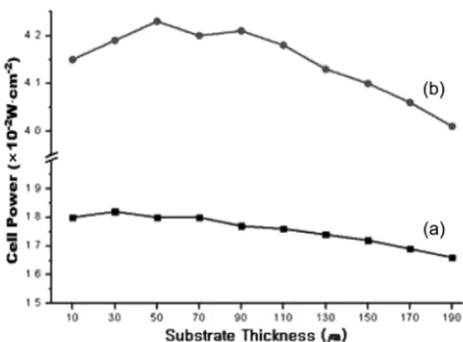
On the effect of the substrate thickness, the p-type sub- strate thickness was changed from 10 µm to 190 µm while the depth of the front pn junction was fixed at 2 µm, As shown in Fig. 2, the cell power changed rather gradually for the thickness range tested: 1.66~1.82 × 10
−2W·cm
−2, or 16.6~18.2 mW·cm
−2, for Si and 40.0~42.3 mW·cm
−2for GaAs. The minor fluctuations in the curves may not be viewed physically significant as they are more likely related to the small variations in grid structuring.
Within the limitation of the minority carrier recombi-
nation lifetime value of 5 × 10
−5sec used in the device simulation, the solar cell power is only weakly dependent on the substrate thickness, particularly under about 100 µm, for both Si and GaAs. Though the optimum sub- strate thickness is about 100 µm or less, the reduction in the power output from the peak value is only about 9%
for Si and 5% for GaAs even when the substrate thick- ness is increased to 190 µm. These interesting results indicate that the substrate thickness is not a major issue in both the slow photon-absorbing indirect-gap Si and the fast photon-absorbing direct-gap GaAs, as long as the materials themselves are pure enough to ensure a long minority-carrier lifetime in the bulk, as was the case in this work. This finding somewhat corroborates an earlier published work in which the BC-BJ Si structure was simulated in terms of the substrate thickness versus the open-circuit voltage (V
OC) for various substrate doping concentrations. For the n-type substrate, as opposed to the p-type in this work, the V
OCvariation was at best about 7%, i.e., 805 mV@10 µm vs. 750 mV@200 µm.
8)Given these findings, for crystalline Si and GaAs with a relatively long recombination lifetime, extra efforts to be spent on thinning the substrate should be weighed against the expected actual gain in the solar cell output power.
Of carrier mobility, minority carrier recombination life- time and photon absorption distance, that are relevant factors in this study, the recombination lifetime seems to have been most influential in causing the weak depen- dency between the substrate thickness and the cell power.
Had the other two factors, where the GaAs is superior by as much as ten times, been more influential, the depen- dency would have been a lot stronger and the downward slope of the curves in Fig. 2, a lot sharper. To further explore this hypothesis, more detailed study on the effect of minority carrier recombination lifetime in conjunction with the substrate thickness on the cell output power is
Fig. 1. The substrate thickness variation: 10 µm(a) vs. 50 µm(b). Thedense (dark) region is the pn junction. The figures are inverted. As such, the metal contacts (unseen) and the pn junction are at the top, and the actual front surface is at the bottom.
Fig. 2. Cell power vs. substrate thickness: the cell power is only weakly dependent on the substrate thickness for both (a) Si and (b) GaAs, particularly under about 100µm.
Simulated Optimum Substrate Thicknesses for the BC-BJ Si and GaAs Solar Cells 453
currently being pursued.
In terms of the peak cell power, GaAs is about 2.3 times more efficient than Si, 42.3 mW·cm
−2vs. 18.2 mW·cm
−2. This seemingly large output power value of GaAs is due to the fact that 0.6 µm single energy photons are used instead of the solar spectrum whereby a large portion has an energy less than the bandgap energy of GaAs. Although the actual cell power difference between GaAs and Si is expected to be much less under the natural solar spectrum, the high efficiency of GaAs leaves a lot of room for engineering in terms of material combination, device design and solar spectrum selection.
4. Conclusion
In this study where the BC-BJ Si and GaAs solar cells are compared one to one by means of the Medici device simulation, GaAs is about 2.3 times more efficient than Si in terms of the peak cell power output, 42.3 mW·cm
−2vs. 18.2 mW·cm
−2, when 0.6 µm photons enter the solar cells at the normal incident angle ( θ = 90
o). This strong performance of GaAs, although under an ideal condition, gives a strong indication that it could stand competitively against Si, despite its known high material and process costs.
Within the limitation of 10 µm-wide BC-BJ solar cell device simulation with a fixed minority carrier recombi- nation lifetime value of 5 × 10
−5sec, the solar cell power is only weakly dependent on the substrate thickness, par- ticularly under about 100 µm, for both Si and GaAs.
Though the optimum substrate thickness is about 100 µm or less, the reduction in the power output is less than 10% from the peak values even when the substrate thick- ness is increased to 190 µm. The reduction may not be deemed insignificant. However, any extra effort to be
spent on thinning the substrate should be carefully weighed against the expected actual gain in the solar cell output power for crystalline Si and GaAs with a re- latively long recombination lifetime.
Acknowledgement
The simulation experiments and the rendering of the graphical work were assisted by the undergraduate students, Mr. Soon-Min Kwon, Mr. Tae-Hoon Jung, Mr. Ki-Yong Kim, Mr. Ji-Min Kim, Mr. Seung-Jin Lee, and Mr. Ju- Yong Park. of the Department of Electronic Materials Engineering of the University of Suwon. The author wishes to thank them for the diligent work as well as the shared good times.
References
1. J. H. Kim, M. J. Chu, Y. D. Chung, R. M. Park and H.
K. Sung, Electronics and Telecommunications Trend Analysis (ETRI), 23(6), 2 (2008) (in Korean).
2. Y. S. Jeon, H. K. Park, H. K. Yun, M. K. Kang and J. D.
Kim, Weekly Technology Trends (IITA), 1335, 21 (2008) (in Korean).
3. F. Dimroth and S. Kurtz, MRS Bulletin, 32, 230 (2007).
4. M. A. Green, K. Emery, D. L. King, Y. Hishikawa and W. Warta, Prog. Photovolt. Res. Appl., 15, 35 (2007).
5. L. L. Kazmerski, J. Electron Spectros. Relat. Phenom., 150, 105 (2006).
6. K. S. Choe, Solid State Sci., 12, 1948 (2010).
7. Medici Two-Dimensional Device Simulation Program (Ver. 2.2); User's Manual, Vol. 3, p. 7.1-7.10, Technology Modeling Associates, Inc., Sunnyvale, CA, USA (1996).
8. F. Granek, Ph. D. Thesis, p. 3, Fraunhofer Institute for Solar Energy Systems (ISE), Freiburg, Germany (2009).