• 검색 결과가 없습니다.

Effect of Substrate Bias Voltage on the Growth of Chromium Nitride Films

N/A
N/A
Protected

Academic year: 2021

Share "Effect of Substrate Bias Voltage on the Growth of Chromium Nitride Films"

Copied!
4
0
0

로드 중.... (전체 텍스트 보기)

전체 글

(1)

[

논 문] 한국재료학회지

Kor. J. Mater. Res.

Vol. 17, No. 11 (2007)

618

Corresponding author

E-Mail : [email protected] (D. I. Kim)

Effect of Substrate Bias Voltage on the Growth of Chromium Nitride Films

Ho Sang Jang, Yu Sung Kim, Jin Hee Lee, Huigon Chun, Yong Zoo You and Daeil Kim

School of Materials Science and Engineering, University of Ulsan, San 29, Nam-Gu, Ulsan, 680-749, Korea

(Received September 3, 2007 : Accepted November 8, 2007)

Abstract Chromium nitride (CrN) films were deposited on silicon substrate by RF magnetron sputtering assisted by inductive coupled nitrogen plasma without intentional substrate heating. Films were deposited with different levels of bombarding energy by nitrogen ions (N

+

) to investigate the influence of substrate bias voltage (V

b

) on the growth of CrN thin films. XRD spectra showed that the crystallographic structure of CrN films was strongly affected by substrate bias voltage. Scanning electron microscopy (SEM) and atomic force microscopy (AFM) results showed that surface roughness and grain size of the CrN films varied significantly with bias voltage. For –80 V

b

depositions, the CrN films showed bigger grain sizes than those of other bias voltage conditions. The lowest surface roughness of 0.15 nm was obtained from the CrN films deposited at –130 V

b

. Key words Chromium nitride; Inductive coupled plasma (ICP); Substrate bias; AFM; XRD.

1. Introduction

Transition metal nitrides such as chromium nitride (CrN) have been proposed as promising hard coating thin films due to their high hardness, wear, corrosion and high temperature oxidation resistance.

1-3)

Currently, ion beam system,

2)

cathodic arc,

4)

and magnetron sputtering

5)

methods have been developed to obtain high rate deposition processes of chromium nitride (CrN) thin films for cost effective industrial applications.

Among these deposition technologies, magnetron sputtering is recommended as an efficient method for the synthesis of high rate deposited CrN films. It has also been reported that the main parameters controlling the properties of CrN films in a magnetron sputtering process are substrate temperature and nitrogen gas partial pressure in a spu- ttering atmosphere.

6)

In this study, CrN films were prepared with a magnetron sputtering system assisted by inductive coupled plasma (ICP). The effect of negative substrate bias voltage (V

b

) on the surface morphology and microstructure of the films was investigated. Microstructures were analyzed by X-ray diffraction (XRD), and surface morphology properties were evaluated by scanning electron microscopy (SEM) and atomic force microscopy (AFM).

2. Experimental procedures

CrN films were deposited on single crystal Si (100) wafers by an RF magnetron sputter assisted by inductive coupled nitrogen plasma. Fig. 1 shows the schematic diagram of the system used in this study. The antenna conductor, which was made of a Cu tube for water cooling, was located on the side wall of the chamber approximately 100 mm from the substrate. To produce N

+

ions, a three turn antenna with a diameter of 200 mm was coupled to a radio frequency (RF) power generator at 13.56 MHz via a matching network. The cylindrical quartz chamber for the N

+

ion source was 180 mm in diameter and 250 mm in length. The RF power for the antenna conductor was kept constant at 100 W. The ionic current density was equal to 6 µ A/cm

2

.

Pure argon (Ar, 99.99%) and nitrogen (N

2

, 99.99%) gas were introduced after the pressure in the chamber was lowered to 1 ×10

−5

Pa. The Ar partial pressure was kept constant at 0.3 Pa, while N

2

partial pressure was kept constant at 0.05 Pa. CrN films were deposited from a pure Cr target (99.99%) by an RF magnetron sputter in an Ar and N

2

atmosphere.

During the deposition process, substrate temperature

was evaluated with a thermal couple located on the back

of the holder plate. Although deposition was carried out

w ith ou t i nten ti on al su bs trate heat in g, su bs trate

temperature increased up to 200 due to the generation of

plasma in the chamber.

(2)

Effect of Substrate Bias Voltage on the Growth of Chromium Nitride Films 619

Cr target power and distance from target to substrate were kept constant at 100 W (power density: 2.5 W/cm

2

) and 100 mm, respectively. Negative substrate bias voltages (–30 V

b

, –50 V

b

, –80 V

b

, –100 V

b

, –130 V

b

) were applied to the substrate by a DC power supply.

Prior to deposition, 10 min of re-sputtering with a sputtering power of 150 W was performed to remove the metal-nitride layer of the target surface due to previous depositions.

Chemical compositions of these films were determined by quantitative energy dispersive X-ray (EDS) analysis using an EDAX DX-4 analyzer. Crystallographic structure was characterized by X-ray diffraction (XRD) using Cu K α radiation. Surface morphology and rms roughness were measured by scanning electron micro- scopy (SEM) and atomic force microscopy (AFM), respectively. Thickness was measured using an Alpha- Step 500 profiler.

3. Results and discussion

Fig. 2 shows the deposition rate at different substrate V

b

. Deposition rates decreased from 15.4 nm/min to 10 nm/min. When the deposition process was carried out

with a negative substrate bias, the N

+

ions of the plasma were attracted towards the substrate holder, thus transferring their kinetic energy to the surface atoms. As seen in Fig. 2, if the incident ion energy, which increased with increasing negative bias voltage, is high enough, this effect may induce a re-sputtering of the coating, giving rise to lower deposition rates.

1)

Nitrogen content in a film also depends on the substrate bias voltage. Nitrogen content measured by EDS was about 49 at % when V

b

= –30 V and 47at% for V

b

= – 130 V. This suggests that the nitrogen content of the deposited films was reduced by high energy ion bom- bardments. This result is in agreement with previous Fig. 1. Schematic illustration of the ICP-assisted RF magnetron

sputtering system.

Fig. 2. Deposition rate as a function of substrate bias voltage.

Fig. 3. XRD spectra for CrN films deposited at various substrate

bias voltages.

(3)

620 Ho Sang Jang, Yu Sung Kim, Jin Hee Lee, Huigon Chun, Yong Zoo You and Daeil Kim

reports by T. Hurkmans et al.

7)

and C. Gautier et al.

8)

Fig. 3 shows XRD spectra of CrN films deposited under different substrate bias voltages. Crystallographic structure of the CrN films was strongly affected by substrate bias voltage. CrN (111) films with FCC structure were grown at V

b

= –30 V. The XRD spectra showed that the phases of CrN films changed from CrN to Cr

2

N + CrSi as a function of substrate bias voltage. At –80 V

b

, the CrN (111) peak disappeared, while a CrN (220) peak appeared in the XRD spectrum. Film deposited at –130 V

b

showed considerably more diffraction peaks, as seen in Fig. 3 (V

b

= –130 V). This is due to growing films being bombarded by energetic ions, which increases nucleation seeds for grain growth.

9)

Fig. 4 shows plain view scanning electron micrographs (SEM) for CrN films deposited at various V

b

conditions.

Thickness of the films was kept constant at 100 nm.

Microstructure was affected by the applied V

b

. The film

deposited with –80 V

b

shows larger grain sizes than those of films deposited at other V

b

conditions. During deposition, N

+

ions transfer their kinetic energy to the surface adatoms. The transferred energy increased the mobility of the adatoms on the surface, and consequently larger grains were formed. However, the grain size of CrN films deposited at –130 V

b

was smaller than that deposited at – 80 V

b

. It is well known that ion bombardment due to biasing the substrate causes a reduction of the grain size.

Ion beam energy that is too intense may increase the concentration of defects and formation of complex defects, thus hindering recrystallization.

10)

Fig. 5 shows AFM images of CrN film deposited at a bias voltage of –50 V

b

. The films show the island growth. In this study, surface average roughness (Ra) of

Fig. 4. Plain view scanning electron micrographs (SEM) for CrN films deposited at various substrates bias voltages: (a) – 30 V, (b) –50 V, (c) –80 V, (d) –100 V, (e) –130 V.

Fig. 6. Surface average roughness (Ra) of the films deposited at various substrate bias voltages.

Fig. 5. Atomic force microscopy (AFM) images for CrN film

surfaces deposited at substrate bias voltage of −50 V.

(4)

Effect of Substrate Bias Voltage on the Growth of Chromium Nitride Films 621

the films was decreased with V

b

due to intense ion beam bombardment. The lowest roughness of 0.5 nm was obtained from CrN films deposited at a bias voltage of – 130 V

b

, as seen in rms data graph (Fig. 6).

4. Conclusion

An ICP-assisted magnetron sputtering system was used to deposit chromium nitride (CrN) films. To investigate the effect of substrate bias voltage on CrN film properties, CrN films were deposited without intentional substrate heating under different substrate bias voltage conditions.

The deposition rate decreased with bias voltage due to intense N

+

ion bombardment. XRD spectra showed that the crystallographic structure of the CrN films was strongly affected by the substrate bias voltage. Grain size and surface roughness were also affected by substrate bias voltage.

References

1. E. Forniés, R. Galindo, O. Sánchez and J. Albella, Surf.

Coat. Technol., 200, 6047 (2006).

2. J. Lim and C. Lee, Mat. Chem. Phys., 95, 164 (2006).

3. O. Banakh, P. Schmid, R. Sanjinés and F. Lévy, Surf. Coat.

Technol., 163, 57 (2003).

4. K. Chang, S. Chung, S. Lai and H. Shih, Appl. Surf. Sci., 236, 406 (2004).

5. A. Ehiasarian, W. Münz, L. Hultman, U. Helmersson and I. Petrov, Surf. Coat. Technol., 163, 267 (2003).

6. C. Gautier, H. Moussaoui, F. Elstner and J. Machet, Surf.

Coat. Technol., 86, 254 (1996).

7. T. Hurkmans, D. Lewis, H. Paritong, J. Brooks and W.

Munz, Surf. Coat. Technol., 114, 52 (1999).

8. C. Gautier and J. Machet, Thin Solid Films, 295, 43 (1997).

9. D. Kim, Appl. Surf. Sci., 218, 79 (2003).

10. D. Kim and S. Kim, Surf. Coat. Technol., 154, 204 (2002).

수치

Fig. 3. XRD spectra for CrN films deposited at various substrate bias voltages.
Fig. 6. Surface average roughness (Ra) of the films deposited at various substrate bias voltages.

참조

관련 문서

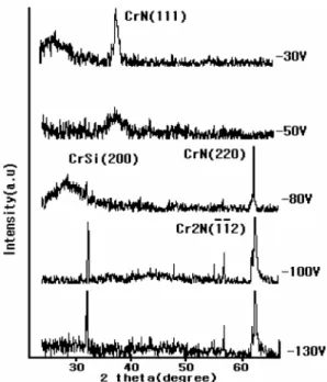
In this study, NiFe films with a thickness of about 150nm were deposited on Si(100) wafer and SiO 2 / Si(100) substrate at room temperature by a DC magnetron co-sputtering using Fe

Titanium oxide (TiO 2 ) films are deposited on the indium tin oxide (ITO) substrate in an Ar/O 2 atmosphere by using reactive RF (Radio Frequency) magnetron

Transparent and conducting titanium doped indium oxide (TIO) thin films were deposited by RF magnetron sputtering on zinc oxide (ZnO)-coated glass substrates to investigate

The results showed that a bias applied to the substrate during sputtering contributed to the improvement of electrical properties of the film by attracting

We have optimized the radio frequency (RF) magnetron sputtering process to produce highly transparent, highly conductive undoped ZnO and GZO films at

Structural, Electrical, and Optical Properties of ZnO:Ga Films Grown by the RF Magnetron Sputtering Method under Different Substrate Temperatures.. Seungmin Park · Youngho

Abstract This study examined the effect of growth temperature on the electrical and optical properties of hydrogenated Al-doped zinc oxide (AZO:H) thin films deposited by

Multi layered film was deposited on a glass substrate at room temperature by DC/RF magnetron sputtering system and EMP (Essential Macleod Program) was adopted