• 검색 결과가 없습니다.

Effect of a ZnO Buffer Layer on the Structural, Optical and Electrical Properties of TIO/ZnO Bi-layered Films

N/A
N/A
Protected

Academic year: 2021

Share "Effect of a ZnO Buffer Layer on the Structural, Optical and Electrical Properties of TIO/ZnO Bi-layered Films"

Copied!
4
0
0

로드 중.... (전체 텍스트 보기)

전체 글

(1)

289

한국표면공학회지 J. Korean Inst. Surf. Eng.

Vol. 52, No. 6, 2019.

https://doi.org/10.5695/JKISE.2019.52.6.289

<연구논문>

ISSN 1225-8024(Print) ISSN 2288-8403(Online)

Effect of a ZnO Buffer Layer on the Structural, Optical and Electrical Properties of TIO/ZnO Bi-layered Films

Su-Hyeon Choe, Yun-Je Park, Jin-Young Choi, and Daeil Kim

*

School of Materials Science and Engineering, University of Ulsan, Ulsan 44776, Korea (Received 23 September, 2019 ; revised 25 October, 2019 ; accepted 19 November, 2019)

Abstract

Transparent and conducting titanium doped indium oxide (TIO) thin films were deposited by RF magnetron sputtering on zinc oxide (ZnO)-coated glass substrates to investigate the effect of the ZnO buffer layer on optical and electrical properties of TIO/ZnO bi-layered films. TIO 90 nm / ZnO 10 nm films having a lower resistivity (3.09×10

-3

Ωcm) and a higher visible transmittance (80.3%) than other TIO/ZnO films were prepared in this study. Figure of merit results indicate that a 10 nm thick ZnO thin film is an effective buffer layer that enhances optical transmittance and electrical conductivity of TIO films without intentional substrate heating or post-deposition annealing.

Keywords: ZnO, TIO, Magnetron sputtering, Hall effect, Figure of merit

1. Introduction

There is considerable interest in use of Ti doped In

2

O

3

(TIO) films as a transparent, conducting oxide (TCO) layer for transparent electrodes because of relatively high visible transmittance and low resistivity [1]. However, high substrate temperature (≥300

o

C) is needed to produce conventional TIO films, with required optical and electrical properties [2]. One way to improve optical and electrical properties of TCO films without substrate heating is to use a TCO/metal/TCO (OMO) structure, with lower resistivity than TCO single layer films [3].

Another strategy that has been used to improve electrical properties of TCO films has been to insert a noble metal buffer layer under the TCO film such as ITO/Au bi-layer film [4]. Also, N. Tiwari reported that insertion of an optimized 60 nm ZnO buffer layer under the IGZO active layer results in enhanced threshold voltage of the transparent thin

film transistor (TTFT) [5].

In this study, TIO/ZnO bi-layered films were deposited by radio frequency (RF) magnetron sputtering on glass substrates. The ZnO buffer layer is an inexpensive and non-toxic oxide material that grows at low temperatures in a wurtzite type hexagonal structure [6]. For these reasons, we investigated the effects of ZnO buffer layer on structural, optical and electrical properties of TIO/

ZnO bi-layer films by using X-ray diffraction (XRD), atomic force microscope (AFM), UV-Visible spectrophotometer, four-point probe and Hall effect measurement system, respectively.

2. Experimental Part

A 100 nm thick TIO single layer and TIO/ZnO bi- layered films were deposited by radio frequency (RF) magnetron sputtering onto glass substrate (Corning 1797, 2×2 cm

2

) at room temperature. TIO (In

2

O

3

:Ti = 95:5 At. %, Purity 99.99%) and ZnO (Purity 99.95%) targets had 3-inch diameter. Glass substrates were degreased in dilute detergent solution, rinsed in de-ionized water and blown dry in nitrogen gas before they were set on the substrate holder. Distance

* Corresponding Author: Daeil Kim

School of Materials Science and Engineering, University of Ulsan, Ulsan 44776, Korea

Tel: +82-52-712-8066 ; Fax: +82-52-712-8045

E-mail: [email protected]

(2)

290 Su-Hyeon Choe et al./J. Korean Inst. Surf. Eng. 52 (2019) 289-292

between the target and substrate was kept at 60 mm for all deposition.

Prior to deposition, the sputter chamber was evacuated to 6.0×10

-7

Torr and then 10 sccm Argon (Ar) gas was injected to optimized deposition pressure of 1.0×10

-3

Torr. During deposition, both targets were biased with a RF magnetron sputtering power of 3 W/cm

2

. By controlling deposition time, TIO/ZnO films with different thickness, namely TIO 90 nm/ ZnO 10 nm, TIO 80 nm/ZnO 20 nm, and TIO 70 nm/ZnO 30 nm were prepared.

After deposition, thickness of the films was confirmed using a surface profiler (Dektak-150, Varian), and crystallinity of films was investigated by XRD (X’pert PRO MRD, Phillips) analysis at the Korea Basic Science Institute (KBSI, Daegu Center).

Optical transmittance in visible wavelength region was evaluated using a UV-visible spectrophotometer (Cary 100 Cone, Varian). Variations in surface morphology (scan area; 3×3 μm

2

) and root mean square (RMS) roughness of films were measured by atomic force microscopy (AFM, XE-100, Park Systems). Electrical properties of films were investigated by four-point probe and Hall measurements system (HMS-3000, Ecopia), respectively.

3. Results and discussions

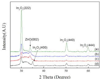
Fig. 1 shows XRD patterns of TIO single layer and TIO/ZnO bi-layer films of different thickness. As deposited TIO thin film shows weak In

2

O

3

(222) and (400) peaks, while all TIO/ZnO films exhibit ZnO (002) and In

2

O

3

(222) peaks in common. As increase thickness of ZnO buffer layer, the peak intensity of In

2

O

3

increases proportionally. Based on XRD patterns in Fig. 1, a thin ZnO buffer layer is effective on preferred orientation growth of upper TIO film at room temperature.

Fig. 2 shows optical transmittance of TIO single layer and TIO/ZnO bi-layered films in visible wavelength range. TIO thin films have lower average transmittance as 77.1%. TIO films have lower transmittance than that of TIO 80 nm/ZnO 20 nm (78.7%) and TIO 90 nm / ZnO 10 nm films (80.3%).

However, TIO 70 nm/ZnO 30 nm films with higher preferred orientation growth mode showed lower visible transmittance of 75.9% in this study.

The rough surface may deteriorate visible transmittance of TCO film but because of increased optical absorption and scattering, surface morphology

is an integral determinant of the optoelectrical performance of TCO films [7].

Fig. 3 shows surface morphologies of TIO single layer and TIO/ZnO bi-layered films. As-deposited TIO film had a flat surface with low RMS roughness value (0.63 nm), while the surface of TIO films with a ZnO buffer layer was rougher and RMS roughness increased with increase in thickness of the ZnO buffer layer. RMS roughness of the TIO 70 nm/ZnO 30 nm films was as high as 1.39 nm. From the AFM images, low visible transmittance of 75.9% at the TIO 70 nm/ZnO 30 nm films is attributed to the Fig. 1. XRD pattern of TIO single layer and TIO/ZnO bi-layered films with different thickness. (a) TIO 70 nm / ZnO 30 nm, (b) TIO 80 nm / ZnO 20 nm, (c) TIO 90 nm / ZnO 10 nm, (d) TIO 100 nm.

Fig. 2. The average optical transmittance of TIO single

layer and TIO/ZnO bi-layered films with different

thickness. (a) TIO 70 nm / ZnO 30 nm, (b) TIO 80 nm /

ZnO 20 nm, (c) TIO 90 nm / ZnO 10 nm, (d) TIO

100 nm.

(3)

Su-Hyeon Choe et al./J. Korean Inst. Surf. Eng. 52 (2019) 289-292 291

rougher surface than those of another film in Fig. 3.

Although presence of a ZnO buffer appeared to increase roughness of TIO/ZnO films, observed RMS roughness of TIO/ZnO bi-layered films was lower than that of conventional ITO single layer films (≤ 0.4 nm).

Table 1 shows electrical properties of TIO single layer and TIO/ZnO bi-layered films. Since the interface between the TIO film and ZnO buffer layer decrease carrier mobility in bi-layered films, TIO/

ZnO films show lower carrier mobility than TIO films. However, TIO 90 nm/ZnO 10 nm films had similar resistivity of 3.09×10

-3

Ω cm with TIO single layer films (2.95×10

-3

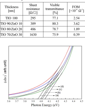
Ω cm). To consider effects of the ZnO buffer layer on optoelectrical performance of the films, figure of merit (FOM) of the TIO and TIO/

ZnO films were compared in Table 2.

The FOM defined by G. Haacke [8] is;

FOM = T

10

/ R□ (1)

Where T is average visible transmittance and R□ is sheet resistance. The 100 nm thick TIO single layer films exhibited an Rs of 295 Ω/ □ and the TIO 90 nm/ZnO 10 nm films exhibited slightly higher Rs of 309 Ω/ □ , respectively. In Table 4, although all TIO/ZnO bi-layer films showed higher sheet resistance than TIO single layer films, TIO 90 nm/

ZnO 10 nm films showed higher FOM (3.62×10

-4

-1

) value due to higher visible transmittance of 80.3%.

Fig. 4 shows a plot of (αhν)

2

of the TIO/ZnO films as a function of photon energy. Optical absorption

coefficient (α) can be calculated from the following equation (2) [9]:

α = (1/d) ln (1/T). (2)

Here, d is the film thickness and T is the visible transmittance. The Tauc formula (3) gives the relationship between optical absorption coefficient (α) and optical band gap (E

g

) [10]:

(αhν)

2

= A (hν - E

g

) (3)

Fig. 3. Surface morphology and RMS roughness of TIO 70 nm / ZnO 30 nm (a), TIO 80 nm / ZnO 20 nm (b), TIO 90 nm / ZnO 10 nm (c) and TIO 100 nm single layer film (d).

Table 1. The electrical properties of TIO single layer and TIO/ZnO bi-layered films with different thickness.

Thickness [nm]

Carrier Concentration

[×10

19

/ cm

3

]

Carrier Mobility [cm

2

/Vs]

Resistivity [×10

-3

Ωcm]

TIO 100 9.82 21.58 2.95

TIO 90/ZnO 10 9.84 20.50 3.09 TIO 80/ZnO 20 6.45 19.89 4.86 TIO 70/ZnO 30 2.49 15.42 16.3 Table 2. Figure of Merit (FOM) of TIO single layer and TIO/ZnO bi-layered films with different thickness.

Thickness [nm]

Sheet resistance

[Ω/ □ ]

Visible transmittance

[%]

FOM [×10

-4

-1

]

TIO 100 295 77.1 2.54

TIO 90/ZnO 10 309 80.3 3.62

TIO 80/ZnO 20 486 78.7 1.89

TIO 70/ZnO 30 1630 75.9 0.39

Fig. 4. Plots of (αhν)

2

as a function of the incident

photon energy(hν) for the films annealed at different

temperatures. The extrapolation of the linear region

determines optical bandgap (E

g

) values as indicated

with lines. (a) TIO 70 nm / ZnO 30 nm; 3.954 eV, (b)

TIO 80 nm / ZnO 20 nm; 3.993 eV, (c) TIO 90 nm /

ZnO 10 nm; 4.044 eV, (d) TIO 100 nm, 4.010 eV

(4)

292 Su-Hyeon Choe et al./J. Korean Inst. Surf. Eng. 52 (2019) 289-292

Here, hν is the energy of the incident photon and A is the absorption edge width parameter.

From observed electrical properties and optical band gap, it can be concluded that the shift of the optical band gap is related to carrier density of the films. The band gap increased from 4.010 to 4.044 eV, with carrier density increasing from 9.82 × 10

19

cm

−3

at TIO single layer films to 9.84 × 10

19

cm

−3

at TIO 90 nm /ZnO 10 nm films.

4. Conclusions

TIO single layer and TIO/ZnO bi-layered films were deposited on glass substrates without intentional substrate heating by RF magnetron sputtering.

Structural and opto-electrical properties of TIO films were dependent on the ZnO buffer layer. TIO 90 nm/

ZnO 10 nm bi-layered films show higher figure of merit than TIO single layer films because of higher visible transmittance of 80.3%. Also, higher optical band gap (4.044 eV) is observed at the TIO 90 nm/

ZnO 10 nm bi-layered films because of increased carrier concentration by insertion of the ZnO buffer layer.

From observed results, it is supposed that presence of an optimal ZnO buffer layer in TIO/ZnO films improves opto-electrical performance relative to that of TIO single layer films.

References

[1] R. K. Gupta, K. Ghosh, S. R. Mishra, P.K. Kahol, Mater. Lett., 62 (2008) 1033.

[2] D. Kim, B. Kim, H. Kim, Thin Solid Films, 547 (2013) 225.

[3] H. Moon, Daeil Kim, Korean J. Met. Mater., 55 (2017) 209.

[4] Y. S. Kim, J. H. Park, Daeil Kim, Vacuum, 82 (2008) 57.

[5] N. Tiwari, H. D. Shieh, P. Liu, Mater. Lett., 151 (2015) 53.

[6] N. Afzal, M. Rafique, M. Imran, R. Ahmad, Ceram.

Inter., 45 (2019) 15547.

[7] H. N. Cui, V. Teixeira, L. J. Meng, R. Martins, E. Fortunato, Vacuum, 82 (2008) 1507.

[8] G. Haacke, J. Appl. Phys., 47 (1976) 4086.

[9] S. Peng, T. Yao, Y. Yang, K. Zhang, J. Jiang, K.

Jin, G. Li, X. Cao, G. Xu, and Y. Wang, Physica B, 503 (2016) 111.

[10] J. Tauc, Amorphous and Liquid Semiconductors,

Plenum, New York, 1974.

수치

Fig. 1 shows XRD patterns of TIO single layer and TIO/ZnO bi-layer films of different thickness
Fig. 3. Surface morphology and RMS roughness of TIO 70 nm / ZnO 30 nm (a), TIO 80 nm / ZnO 20 nm (b), TIO 90 nm / ZnO 10 nm (c) and TIO 100 nm single layer film (d).

참조

관련 문서

The purpose of this study is to investigate the effect of the “problem solving and programming” area of ​​information subject on perception and

Objectives: This study aimed to investigate the relationship between job stress and turnover intention of employed opticians and to investigate the mediating effect of burnout

The purpose of this study is to investigate the effect of peer-mentoring on the achievement and learning attitudes of middle school students toward

Lee, “Effective Ag Doping by He-Ne Laser Exposure to Improve the Electrical and the Optical Properties of CdTe Thin Films for Heterostructured Thin Film

Decomposition (MOD) process, and then the zinc oxide nanorods on ZnO seed layer were grown by hydrothermal process from 0.3 M at pH 7, 80 ℃ , 1 h. Single phase zinc oxide

Improvement of the Performance and Stability of Oxide Semiconductor Thin-Film Transistors Using Double-Stacked Active Layers.. Metal oxide semiconductor

The laser-induced doping of Al into CdTe thin films is very simple and effective to dope a multilayered thin film solar cell with a relatively short

We report the fabrication of nano-porous ZnO nanowires (NWs) using a process combining laser-induced hydrothermal growth followed by a post annealing process.. Initially,