Phase transformation and magnetic properties of NiFe thin films on Si(100) wafer and SiO 2 /Si(100) substrate by co-sputtering
Dae Sik Kang, Jong Han Song, Joong Hee Nam, Jeong Ho Cho and Myoung Pyo Chun
†Electronic Components Center, Optic & Electronic Center Division, Korea Institute of Ceramic Engineering and Technology, Seoul 153-801, Korea
(Received August 27, 2010) (Revised October 5, 2010) (Accepted October 7, 2010)
Abstract Ni-Fe alloys have various applications such as thin film inductor, thin film transformer, magnetic head’s shield case, etc. Magnetic properties of Ni-Fe thin films depend on the process parameters such as thickness, contents, deposition rate, substrates, etc. In this study, NiFe films with a thickness of about 150nm were deposited on Si(100) wafer and SiO
2/ Si(100) substrate at room temperature by a DC magnetron co-sputtering using Fe and Ni targets. Their phase formation and magnetic properties as a function of annealing temperature were investigated with XRD, FE-SEM and VSM. The as- sputtered films have BCC structure. With increasing annealing temperature, NiFe thin film for SiO
2/Si(100) substrate transformed completely from BCC to FCC phase above 500
oC, but some BCC phase remained above 500
oC on Si(100) wafer. For samples annealed at 450
oC, squareness ratio of NiFe thin film shows peak value and its saturation magnetization is around 0.0118 emu, which means that the optimum annealing temperature of NiFe thin film seems to be 450
oC. The saturation magnetization of films decreased rapidly above the annealing temperature of 500
oC due to phase transformation from BCC to FCC phase.
Key words Soft-magnetic, Phase transformation, NiFe
Si(100) wafer와 SiO 2 /Si(100) 기판에 동시 스퍼터링법으로 증착된 NiFe 합금 박 막의 상변화 및 자기적 특성
강대식, 송종한, 남중희, 조정호, 전명표
†한국세라믹기술원 광·전자세라믹본부 전자부품센터, 서울, 153-801 (2010 년 8월 27일 접수)
(2010 년 10월 5일 심사완료) (2010 년 10월 7일 게재확정)
요 약 Si(100) wafer와 SiO
2/Si(100) 웨이퍼에 증착된 NiFe 합금 박막의 결정상과 자기적 특성을 비교하고자 동시 스퍼 터링법을 이용하여 두 기판 위에 150 nm의 박막을 제조하여 그의 상변화와 자기적 특성을 XRD, FE-SEM, VSM으로 비교 하였다. 두 기판 위에 증착된 NiFe 박막은 BCC상으로 증착되었으나 400
oC 에서 2시간 열처리를 한 결과 BCC에서 FCC로 의 상전이가 일어나는 것을 관찰 할 수 있었으며 Si(100) wafer위에 증착된 박막에서는 500
oC 에서 열처리 후에도 BCC와 FCC 가 혼재하여 나타나는 것을 알 수 있었다. 450
oC 에서 열처리 하였을 때 각형비가 가장 높았으며 포화자화는 0.0118 emu 로 나타나고 있었다. 500
oC 이상의 온도에서는 상전이로 인해 포화자화가 급격히 감소하는 것을 볼 수 있었다.
1. 서 론
NiFe 계 합금은 높은 투자율 및 낮은 보자력을 가지는 대표적인 연자성 재료로써, 가공성이 우수하여 오래전부
터 많은 연구가 이루어져 왔으며, 특히, 전자기적 특성 및 미세구조의 향상을 위해 다양한 조성 및 공정연구가 있었다[1]. NiFe계 합금은 이러한 우수한 자기적 특성 및 가공성을 바탕으로 자기 헤드, 스위치 전원, 자기 메 모리 소자, MEMS 등과 같은 여러 다양한 분야에서 응 용이 되어 지고 있다[2, 3].
NiFe 합금은 Ni과 Fe의 함량에 따라 BCC와 FCC 구 조를 가지며, Ni 함량이 증가하면 BCC구조에서 FCC구
†
Corresponding author
†
Tel: +82-2-3282-2429
†
Fax: +82-2-3282-7769
†
E-mail: [email protected]
조로의 상변화가 나타난다. NiFe 박막의 경우에는 BCC 와 FCC의 상변화가 일어나는 조성의 범위가 기판의 종 류에 따라 변화된다는 많은 보고가 있다. Quartz 기판위 에 NiFe 박막을 Sputtering으로 증착한 경우, Ni 함량이 19~27.5 % 일 때 BCC 구조로 증착되고, Ni 함량이 46 % 이상일 경우는 FCC 구조로 증착이 되며, 그 사이 의 조성범위에서는 BCC와 FCC가 혼재된 상태로 증착 이 된다[4]. 폴리에스테드 기판에 증착하게 되면 Ni 함 량이 40 % 이하일 경우 BCC 구조로 40~50 %일 경우 BCC 와 FCC가 같이 나타나며 50 % 이상일 때 FCC 구 조로 증착이 된다[5]. MgO(001)를 기판으로 하여 증착 한 경우에는 5~10 nm의 BCC구조위에 FCC구조로 증착 이 된다고 발표되었다[6, 7].
본 연구에서는 Ni
50Fe
50박막의 결정상 형성 및 자기적 특성에 대한 기판 및 열처리 온도의 영향을 조사하기 위 해 Si(100) 웨이퍼와 SiO
2/Si(100) 기판의 2종류의 기판 위에 동시 Sputtering법을 사용하여 NiFe 박막을 증착하 고, 열처리 온도에 따른 상변화 및 자기적 특성을 비교 분석하였다.
2. 실험방법
동시 스퍼터링 법으로 10 × 10 mm의 NiFe 박막을 증 착하기 위해 직경 4 inch의 Fe(99.95 %)와 Ni(99.99 %) 을 타겟으로 사용하고 Fig. 1과 같이 RF-DC 마그네트 론 스터터링 시스템(KOREA VACUUM TECH., LTD) 의 두 개의 DC 마그네트 스퍼터건을 사용하여 동시 증 착하였다. 초기 진공은 2 × 10
−6torr 으로 하여 고순도의 Ar 가스(99.999 %)를 30 sccm으로 주입하여 5 mtorr에 서 Ni 타겟의 출력은 50 W로 Fe 타겟의 출력을 150 W
로 증착하였으며, 이때 균일한 조성의 박막을 얻기 위하 여 기판을 6 rpm의 속도로 회전하였다. 기판으로는 p-type 의 Si(100) 웨이퍼와 열산화 된 SiO
2/Si(100) 웨이퍼를 사용하였으며 기판은 아세톤, 에탄올, 증류수 순으로 각 10 분씩 초음파 세척하여 사용하였고 증착된 상의 변화를 관찰하기 위해서 150 nm의 두께로 증착하였다. 증착 후 챔버에서 5 × 10
−6torr 의 진공을 유지하여 300~500
oC 에 서 2시간 동안 열처리하여 상 분석 및 미세구조 관찰하 기 위하여 XRD(PANalytical, X’pert Pro)와 FE-SEM을 사용하였으며, 진동자력계(LakeShore, Model 7307)를 사용하여 자기적 특성을 비교하였다.
3. 실험결과
3.1. 미세구조 및 상분석
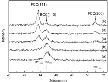
Si(100) 웨이퍼 위에 증착된 NiFe 박막을 열처리 하여 XRD 로 상분성 한 결과를 Fig. 2에 나타내었다. Fig.
2(a) 의 as-sputtered NiFe 박막은 준안정상인 BCC구조의 (110) 면으로 증착되어 있음을 보여주나, Fig. 2(c)의 400
oC 이상에서 열처리 하였을 때 준안정상인 BCC에서 안정 상인 FCC로의 상전이로 인하여, FCC(111)과 (200)면으 로의 성장이 나타나고 있다. 한편, Fig. 2(e)의 500
oC 에 서 열처리할지라도 BCC (110) 상이 완전히 사라지지 않고 상일부가 존재함으로써 상전이 된 FCC상과 잔류 BCC 상이 혼재된 상태를 보여주고 있다.
XRD 데이터를 바탕으로 계산한 결과 NiFe BCC (110) 면의 면간거리는 2.01 Å이고 FCC (111) 면의 면간
Fig. 1. Schematic drawing of the targets and substrate arrange- ments.
Fig. 2. XRD patterns of NiFe thin films on Si(100) wafer vs.
annealing temperature. (a) as-sputtered, (b) annealed at 300
oC, (c) annealed at 400
oC, (d) annealed at 450
oC and (e) annealed at 500
oC. JCPDS No. of FCC (solid line) and BCC (dash line)
NiFe are 01-071-8322 and 00-037-0474 respectively.
거리는 2.07 Å 였으며 Si (100)면의 면간거리는 5.43 Å 이므로 Si 격자 1개당 BCC 상의 NiFe 격자 3개가 있 는 것이 더 안정되기 때문에 기판과 웨이퍼 계면에 있는 BCC 상의 NiFe는 FCC 구조로 상변화가 진행 되지 않 는 것으로 사료되어 진다[6].
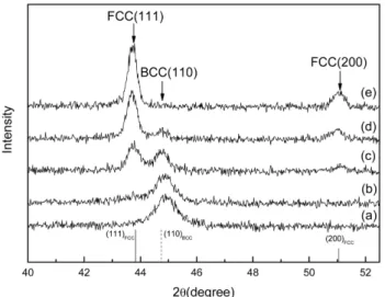
Fig. 3 은 SiO
2/Si(100) 기판에 증착된 NiFe 박막의 열 처리 온도에 따른 상분석 결과로 450
oC 이하에 열처리 한 경우에는 Si(100) wafer에 증착된 NiFe 박막과 비슷 하나 Fig. 3(e)의 500
oC 에서 열처리한 시편에서는 BCC 구조에서 FCC 구조로의 상전이가 모두 진행 되는 것을 알 수 있었다.
Fig. 4 는 열처리 온도에 따른 박막의 표면 사진으로 열처리 온도에 따라 표면에 존재하고 있던 망상 구조의 기공들이 사라지며 박막의 치밀화 및 결정성장이 이루어 지고 있는 것을 알 수 있었다.
3.2. 자기적 특성
VSM 으로 열처리된 박막의 자기적 특성을 분석하여 자기이력곡선을 Fig. 5에 각각 나타내었다. 두 기판에 모두 증착된 박막에서는 경자성체의 자기이력곡선이 나 타나고 있었지만 열처리 온도가 450
oC 까지 증가함에 따 라 연자성체의 자기이력곡선으로 변화 하는 것을 볼 수 있었고 큐리 온도인 500
oC 에서 열처리 한 경우에는 다 시 경자성체의 자기이력곡선으로 변화하는 것을 볼 수 있었다.
자기이력곡선의 변화를 자세히 보기위하여 각형비(M
r/ M
s) 를 계산하여 Fig. 6에 나타내었다. 두 기판 위에 증
착된 NiFe을 450
oC 까지 열처리 하였을 때에는 각형비가 증가하였지만 큐리 온도인 500
oC 에서 열처리 한 경우에 는 감소하고 있었다.
Fig. 7 은 열처리 온도에 따른 포화 자화 값의 변화로 Si(100) wafer 에 증착한 경우 열처리 온도가 400
oC 까지 는 포화 자화 값이 증가하고 있으나 450
oC 이상에서는 감소하는 경향을 보이고 있었다. 열처리 온도 450
oC 에서 Fig. 4. Surface images of NiFe thin films by co-sputtered on Si(100) wafer (a), and SiO
2/Si(100) substrate (b) with annealing
temperature.
Fig. 3. XRD patterns of NiFe thin films by co-sputtered on SiO
2/Si(100) substrate vs. annealing temperature.(a) as-sput- tered, (b) annealed at 300
oC, (c) annealed at 400
oC, (d) annealed at 450
oC and (e) annealed at 500
oC. JCPDS No. of FCC (solid line) and BCC (dash line) NiFe are 01-071-8322
and 00-037-0474 respectively.
는 BCC 구조에서 FCC 구조로의 상전이로 인한 보어자 자(Bohr magneton)의 감소에 의한 영향으로 사료되어지 며[8] 큐리 온도인 500
oC 에서 열처리한 경우의 경자성 체로 돌아가며 포화 자화 값이 떨어지고 있었다.
SiO
2/Si(100) 기판에 증착 된 NiFe 박막의 경우 열처 리 온도가 450
oC 까지는 포화 자화 값이 서서히 감소하 였지만 500
oC 에서 열처리 한 경우에는 급격하게 감소하 는 것을 볼 수 있었다. 두 기판에서 열처리 온도에 따른 포화 자화 값의 변화의 차이로는 열처리 온도에 따라 발 생하는 상변화의 정도가 달라 박막 내의 보어자자의 량 의 차이에 기인하는 것으로 사료되어 진다.
4. 결 론
NiFe 박막 형성에 대한 기판의 영향을 조사하기 위해 Si(100) 웨이퍼와 SiO
2/Si(100) 의 2종류의 기판위에 co- sputtering 법으로 NiFe 박막을 Fe와 Ni Target을 가지고 증착하였다. 증착 직후(as-sputtered)에 준안정상인 BCC 구조의 NiFe 박막은 열처리 온도가 400
oC 이상으로 증 가되면 안정상인 FCC로의 상전이가 XRD 패턴에서 관 찰되었으며, 또한, 자기히스테리시스 측정을 통하여 경자 성체에서 연자성체로의 변화도 관찰되었다. 포화자화 (M
s) 는 증착 직후에는 SiO
2/Si(100) 기판이 Si(100) 웨이 퍼에 비하여 높으나, 열처리 온도가 증가함에 따라 Si(100) 웨이퍼 상의 NiFe박막이 SiO
2/Si(100) 기판에 비하여 높은 포화자화 값을 보이고 있다. 기판의 종류에 따른 이러한 포화자화 값의 변화는 열처리 후에도 존재 하는 Si(100) 웨이퍼 상의 NiFe 박막 내의 잔류 BCC 상의 영향으로 사료된다. 연자성의 NiFe 박막을 얻기 위 해서는 최대의 각형비와 적정한 포화 자화 값을 보이는 Fig. 5. Magnetic hysteresis curves of NiFe thin films by
co-sputtered on Si(100) wafer (a), and SiO
2/Si(100) substrate (b) with annealing temperature.
Fig. 7. Saturation magnetization of NiFe thin films by co-sput- tered on Si(100) wafer and SiO
2/Si(100) substrate with annealing
temperature.
Fig. 6. Squareness ratio of NiFe thin films by co-sputtered on Si(100) wafer and SiO
2/Si(100) substrate with annealing
temperature.
450
oC 에서 열처리하는 것이 좋을 것으로 판단된다.
참 고 문 헌