1. 서 론
기존의 실리콘 반도체와 비교하여 우수한 특성을 지 니는 비정질 산화물 반도체(amorphous oxide semicon- ductor, AOS)는 flexible display, AM-LCD와 AM-OLED 등과 같은 차세대 디스플레이의 백플레인에서 최근 많은 주목을 받아오고 있다 [1-3]. 특히 산화아연(ZnO)을 기반 으로 한 AOS 박막 트랜지스터(thin film transistor, TFT)는 높은 전계효과 이동도(field effect mobility, μFE), 높은 온오프 전류비(Ion/off), 낮은 subthreshold swing
✉ Sang Yeol Lee; [email protected]
Copyright ©2019 KIEEME. All rights reserved.
This is an Open-Access article distributed under the terms of the Creative Commons Attribution Non-Commercial License (http://creativecommons.org/licenses/by-nc/3.0) which permits unrestricted non-commercial use, distribution, and reproduction in any medium, provided the original work is properly cited.
(S.S.), 그리고 좋은 균일성 등과 같은 수많은 장점을 가 지고 있다 [4]. 다양한 비정질 산화물 물질 중에서도 인 듐과 갈륨(In-Ga)이 함유된 비정질 인듐-갈륨-징크-옥 사이드(a-IGZO) TFT의 경우 연구가 상당히 진행되어 있는 상태이다. a-IGZO의 원소 중 하나인 In3+의 경우 최 외각 전자 중 방향에 따른 비등방성이 가장 작은 s-orbital overlap이 일어나게 되어 μFE 향상 기여에 큰 역할을 한다 [5]. 또한 Ga의 경우 훌륭한 캐리어 억제제로서 비 정질 산화물 물질 내부에서 안정성을 향상시키는 역할을 한다 [6]. 하지만 a-IGZO 채널 내부의 In과 Ga은 희토 류이며, 특히 In의 경우 독성을 가지고 있어 큰 단점을 가지고 있다. 이러한 문제를 해결하기 위하여 본 연구그 룹에서는 이전부터 ZnO를 기반으로 하여 μFE 향상을 위 한 주석(Sn)과, 안정성 향상을 위한 실리콘(Si)을 첨가한 비정질 실리콘-아연-주석-산소(a-SZTO)의 특성에 관
비정질 산화물 SiZnSnO 반도체 박막의 전기적 특성 분석
변재민1,2, 이상렬1,2
1 청주대학교 반도체공학과
2 차세대반도체융합기술연구소
Investigation on Electrical Property of Amorphous Oxide SiZnSnO Semiconducting Thin Films
Jae Min Byun
1,2and Sang Yeol Lee
1,21 Department of Semiconductor Engineering, Cheongju University, Cheongju 28503, Korea
2 Research Institute of Advanced Semiconductor Convergence Technology, Cheongju 28503, Korea
(Received May 16, 2019; Revised May 29, 2019; Accepted May 30, 2019)
Abstract: We investigated the electrical characteristics of amorphous silicon-zinc-tin-oxide (a-SZTO) thin films deposited by RF-magnetron sputtering at room temperature depending on the deposition time. We fabricated a thin film transistor (TFT) with a bottom gate structure and various channel thicknesses. With increasing channel thickness, the threshold voltage shifted negatively from -0.44 V to -2.18 V, the on current (Ion) and field effect mobility (μFE) increased because of increasing carrier concentration. The a-SZTO film was fabricated and analyzed in terms of the contact resistance and channel resistance. In this study, the transmission line method (TLM) was adopted and investigated. With increasing channel thickness, the contact resistance and sheet resistance both decreased.
Keywords: Amorphous oxide semiconductor, Thin film transistor, RF sputtering, a-SZTO, Transmission line method
Regular Paper 272
J. Korean Inst. Electr. Electron. Mater. Eng.
Vol. 32, No. 4, pp. 272-275 July 2019 DOI: https://doi.org/10.4313/JKEM.2019.32.4.272 ISSN 1226-7945(Print), 2288-3258(Online)
전기전자재료학회논문지, 제32권 제4호 pp. 272-275, 2019년 7월: 변재민 등 273
해 연구하였다 [7-9]. 특히 온도 변화 [7], 공정 압력 변화 [8], 그리고 실리콘의 함유량 차이 [9] 등에 관한 연구를 주로 진행하였다. 하지만 증착 시간의 변화 에 따른 전기적 특성 변화 및 채널의 저항(channel resistnace, Rch)과 접촉 저항(contact resistance, Rc) 의 변화는 자세히 조사되지 않았다.
따라서 본 논문에서는 a-SZTO 박막의 증착 시간을 달리하여 소자를 제작하였다. 증착 시간이 증가함에 따 라 채널의 두께가 증가하며 그에 따른 전기적 특성 및 선접촉저항분석법(transmission line method, TLM) 을 활용하여 Rch와 Rc를 분석하였다.
2. 실험 방법
본 연구에서는 a-SZTO의 증착 시간에 따른 특성 변 화를 체계적으로 확인하기 위하여 3분에서 7분까지 2 분 간격으로 증착을 진행하였다. 이때 기판으로는 고농 도로 도핑된 P+-Si 기판 위에 200 nm의 SiO2가 게이 트 절연체로 사용된 기판을 사용하였다. 1 wt%의 Si이 도핑된 ZTO (Zn:Sn 비=65:35 wt%) 타입의 a-SZTO 타겟으로 RF-magnetron sputtering 방식을 이용하여 박막을 증착하였다. 공정 조건은 다음과 같다. 3×10⁻³ Torr의 공정 압력, 아르곤:산소=40:1 sccm의 가스 유량비, 그리고 60 W의 파워로 상온에서 증착되었다.
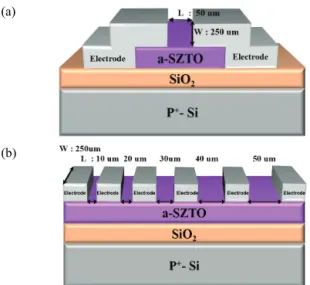
TFT와 TLM 모두 습식 에칭 공정을 통하여 에칭하였 다. 에칭 이후 채널의 안정성 및 활성화, 전극과의 접
촉 특성을 향상시키기 위하여 2시간 동안 500℃에서 대기 분위기에서 후열처리를 진행하였다. 소스와 드레 인 전극은 전자빔 증착법과 열 증착법을 사용하여 각각 티타늄을 10 nm, 알루미늄을 40 nm만큼 증착한 이후 lift-off 방식을 이용하여 제작되었다. 그림 1의 경우 bottom gate 형태의 a-SZTO TFT와 TLM 구조의 개 략도를 나타낸다. 모든 채널의 폭(width, W)은 250 μm 이며 TFT에서의 길이(legth, L)는 50 μm이다. TLM에 서의 경우 L에 따른 분석을 진행하였는데, 10~100 μm까 지 10 μm 기준으로 변경하며 측정하였다. 채널 및 전극 공정은 포토리소그래피 방식을 통하여 제작되었으며 측 정은 빛을 차단하기 위해 암실에서 semiconductor parameter analyzer인 EL423을 사용하여 측정하였다.
3. 결과 및 고찰
그림 2는 드레인-소스 전압(Vd)은 5.1 V에서의 증착 시간에 따른 TFT 소자의 transfer curve를 나타낸다.
이때 게이트-소스 전압(Vg)의 경우 -20~40 V까지 0.2 V 간격으로 측정을 진행하였으며 증착 시간의 변화에 따라 특성 변화가 명확히 나타나는 것을 확인할 수 있 다. 증착 시간이 증가함에 따라 μFE가 21.25에서 23.63 cm2/Vs로 증가하는 것을 알 수 있으며 μFE는 아래의 식 (1)을 통하여 추출하였다 [10].
(1)
gm은 트랜스컨덕턴스, Cox는 게이트 절연체의 산화 캐패시턴스이다.
Fig. 2. The transfer curve of a-SZTO TFT as a function of channel thickness.
(a)
(b)
Fig. 1. The bottom gate schematic structure of the (a) TFT and (b) TLM.
J. Korean Inst. Electr. Electron. Mater. Eng., Vol. 32, No. 4, pp. 272-275, July 2019: J.-M. Byun et al.
274
각 소자와 관련된 전기적 특성은 표 1에 정리하였다.
문턱전압(threshold voltage, Vth)은 -0.44에서 -2.18 V
로 점차 음의 전압 쪽으로 이동함을 나타냈다. 이러한 원 인으로는 증착 시간이 증가함에 따라 채널의 두께가 증 가하게 되며 박막 내 결함인 산소공공(oxygen vacancy, VO)이 증가하게 되어 carrier가 증가하기 때문이다 [11].
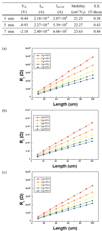
소자의 Rc 및 채널의 면저항(sheet resistance, Rsh)을 분석하기 위하여 TLM 분석을 진행하였다. 채널 L에 따 라 Vg는 40~60 V까지 5 V 간격으로, Vd의 경우 -2~2 V까지 변화를 주며 전류 값 측정을 진행하였다. 이때 채널 L에 따른 I-V 그래프에서 저항만을 추출하여 그 림 3에 L에 따른 전체 저항(total resistance, Rt)을 표기하였다. Rt는 증착 시간이 증가함에 따라 감소하는 것을 확인할 수 있었다. 그림 3에서의 각각의 그래프 에서는 아래의 식 (2)를 통해 Rc 값과 채널의 저항 (channel resistnace, Rch) 값을, W/L을 이용하여 Rsh 값을 추출하였다 [12].
(2)
이와 같은 결과를 그림 4에 도식화하였다. 증착 시 간이 증가함에 따라 Rc 값과 Rsh 값 모두 감소하는 것 을 확인하였다. 증착 시간이 증가함에 따라 접촉 면적 (a)
(b)
(c)
Fig. 3. The total resistances as a function of the channel length with various Vg were measured using the transmission line method (TLM) depending on the deposition time, (a) 3 min, (b) 5 min, and (c) 7 min.
(a)
(b)
Fig. 4. The (a) Rc and (b) Rsh depending on the deposition time.
Vth
(V)
Ion
(A)
Ion/off
(A)
Mobility (cm2/VS)
S.S.
(V/decade) 3 min -0.44 2.18×10⁻⁴ 2.07×10⁸ 21.25 0.38 5 min -0.93 2.27×10⁻⁴ 5.39×10⁹ 22.27 0.43 7 min -2.18 2.40×10⁻⁴ 6.06×10⁷ 23.63 0.44 Table 1. The electronic characteristics of a-SZTO depending on the deposition time.
전기전자재료학회논문지, 제32권 제4호 pp. 272-275, 2019년 7월: 변재민 등 275
이 넓어져 Rc 값은 점차 감소함을 보였으며 Rsh의 경 우 채널 내부의 carrier가 증가하게 되고 그에 따른 저항의 감소를 나타내었다.
4. 결 론
본 논문에서는 증착 시간에 따른 a-SZTO TFT와 TLM을 제작하여 전기적 특성 분석을 진행하였다. 증 착 시간이 증가함에 따라 채널의 두께가 증가하며 그 에 따른 VO의 증가로 인하여 전기적 특성이 향상되었 다. 채널 전도성이 높아짐에 따라 Vth가 음의 방향으로 이동하는 경향과 μFE가 체계적으로 증가하는 것을 확 인하였다. 또한 TLM 방법을 통하여 RC와 Rsh 분석을 진행하였는데 증착시간이 늘어남에 따라 두 값 모두 감소하는 것을 체계적으로 분석하였다. 특히 증착 시간 에 따라 영향이 크게 미치는 것을 확인함으로써 추후 세밀한 연구를 통해 향상된 특성을 자세히 분석할 예 정이다.
ORCID
Sang Yeol Lee https://orcid.org/0000-0002-4405-9042
감사의 글
This work was supported by the research grant of Cheongju University(2017.09.01.~2019.08.31.).
REFERENCES
[1] J. K. Jeong, Semicond. Sci. Technol., 26, 034008 (2011). [DOI:
https://doi.org/10.1088/0268-1242/26/3/034008]
[2] Y. Chen, D. Geng, and J. Jang, IEEE J. Electron Devices Soc., 6, 214 (2018). [DOI: https://doi.org/10.1109/jeds.2018.2790954]
[3] T. Hirao, M. Furuta, H. Furuta, T. Matsuda, T. Hiramatsu, H.
Hokari, M. Yoshida, H. Ishii, and M. Kakegawa, J. Soc. Inf.
Disp., 15, 17 (2007). [DOI: https://doi.org/10.1889/1.2451545]
[4] E. Fortunato, P. Barquinha, and R. Martins, Adv. Mater., 24, 2945 (2012). [DOI: https://doi.org/10.1002/adma.201103228]
[5] K. Nomura, H. Ohta, A. Takagi, T. Kamiya, M. Hirano, and H. Hosono, Nature, 432, 488 (2004). [DOI: https://doi.org/
10.1038/nature03090]
[6] C. L. Tien, K. C. Yu, T. Y. Tsai, and M. C. Liu, Appl. Surf.
Sci., 354, 79 (2015). [DOI: https://doi.org/10.1016/j.apsusc.2015.
02.154]
[7] K. M, Ko and S. Y. Lee, J. Korean Inst. Electr. Electron.
Mater. Eng., 27, 282 (2014). [DOI: https://doi.org/10.4313/
JKEM.2014.27.5.282]
[8] S. Y. Lee, J. Korean Inst. Electr. Electron. Mater. Eng., 25, 580 (2012). [DOI: https://doi.org/10.4313/JKEM.2012.25.8.580]
[9] E. Chong, I. Kang, C. H. Park, and S. Y. Lee, Thin Solid Films, 534, 609 (2013). [DOI: https://doi.org/10.1016/j.tsf.2013.
02.033]
[10] P. B. Shea and J. Kanicki, J. Appl. Phys., 98, 014503 (2005). [DOI: https://doi.org/10.1063/1.1949713]
[11] B. H. Lee and S. Y. Lee, Phys. Status Solidi A, 215, 1700698 (2018). [DOI: https://doi.org/10.1002/pssa.201700698]
[12] C.P.T. Nguyen, T. T. Trinh, J. Raja, A.H.T. Le, Y. J. Lee, V. A. Dao, and J. Yi, Mater. Sci. Semicond. Process., 39, 649 (2015). [DOI: https://doi.org/10.1016/j.mssp.2015.05.069]