Effect of Ga-doping on the properties of ZnO films grown on glass substrate at room temperature
by radio frequency magnetron sputtering
G.C. Kim
1, S.K. Lee
1, J.S. Lee
1, D.H. Kim
1, S.H. Lee
2, J.H.Moon
2, M.H. Jeon
1ϯ1ϯ
Department of Nano Systems Engineering, Center for Nano Manufacturing, Inje University, Gimhae 621-749
2
Department of Materials Science and Engineering, Yonsei Univeristy, Seoul 120-749 (Received January 10, 2008)
We present the effect of Ga-doping on the electrical, structural and optical properties of ZnO layers with a thickness of ~500 nm deposited on glass substrates. Polycrystalline ZnO and Ga-doped ZnO (GZO) layers were deposited by radio frequency (rf) magnetron sputtering at room temperature. Based on the X-ray diffraction (XRD) and transmission electron microscopy (TEM) data, the crystalline quality of Ga-doped ZnO film was improved and GZO film has a preferred orientation along with the (002) crystal direction. The transmittance of the GZO film was enhanced by 10% in the visible region from that of the ZnO film. From photoluminescence (PL) data, the ratio of intensity of near band edge (NBE) emission to deep level (DL) emission was as high as 2.65:1 and 1.27:1 in the GZO and ZnO films, respectively. The res istivities of GZO and ZnO films were measured to be 1.27 and 1.61 Ω·cm, respectively. The carrier concentrations of ZnO and GZO film were approximately 1018 and 1020 ㎠/Vs, respectively. Based on our experimental results, the Ga-doping improves the electrical, structural and optical properties of ZnO film with potential application.
Keywords: ZnO, Ga doping, Glass substrate, Room temperature, rf magnetron sputtering
Ⅰ. Introduction
Zinc Oxide is a wide band-gap semiconductor with a band-gap of 3.37 eV at room temperature and has a large exiciton binding energy (60 meV). Therefore, it is known to be a suitable candidate for the next generation optoelectronic devices such as light emitting devices and laser diodes. Recently, transparent conducting oxide films based on ZnO are receiving much attention because of such advantages
over the more commonly used TCO on cost, resource
availability, non-toxicity and high thermal/chemical
stability [1]. Non-doped ZnO usually presents high
resistivity due to low carrier concentration. Unlike
the non-stoichiometric ZnO films, n-type doped ZnO
films display stable electrical and optical properties
[2]. In ZnO films, doping with Ga species is
particularly effective in stabilizing lattice systems,
less reactive and more resistant to oxidation
compared to Al dopant [3-5]. Several techniques have
been used to grow ZnO films: metal organic chemical vapour deposition, evaporation, magnetron sputtering, sol gel, and plasma assisted molecular beam epitaxy[6]. However, most of those techniques need to use moderate temperatures to obtain low values of resistivity. By rf magnetron sputtering, it is possible to produce highly conductive and transparent gallium-doped zinc oxide (GZO) without heating the substrate, since additional energy is delivered from the plasma to the growing film - a characteristic of a plasma assisted process.
In this study, we deposited both ZnO and GZO thin films on the glass substrate at room temperature by rf magnetron sputtering in order to realize low-cost, transparent devices. We have optimized the radio frequency (RF) magnetron sputtering process to produce highly transparent, highly conductive undoped ZnO and GZO films at room temperature.
The electrical, structural and optical properties of both ZnO and GZO thin films were measured and compared.
Ⅱ. Experimental Methods
Both ZnO and GZO films were deposited on a standard glass substrate at room temperature by radio frequency (rf) magnetron sputtering using a ZnO target and a 2-inch GZO (1 wt. %) target.
Deposition of films was carried out in an argon atmosphere at rf power of 75 W, 5 mTorr pressure at room temperature. The sample holder was fully rotated to ensure uniformity during deposition. Under these growth conditions, the deposition rate was measured to be about 3.5 nm/min for both ZnO and GZO layers. Structural properties were examined by X-ray diffraction (XRD) on a Philips X’Pert PRO diffractometer (40 kV, 30 mA) using Cu Kα1 radiation and transmission electron microscopy(TEM: JEOL 200K). Photoluminescence (PL) spectra were also
recorded at room temperature and a He-Cd laser (325nm) was employed as an excitation source.
Optical transmittance measurements were performed with a UV-VIS-NIR spectrophotometer (Cary 5000 Varian) at wavelengths of 200-1400 nm and electrical properties of the films were determined by Hall-effect measurements.
Ⅲ. Results and Discussions
The structural quality of both ZnO and GZO films on glass substrates were investigated by transmission electron microscope (TEM) and high-resolution X-ray diffraction measurements (HRXRD).
Figure 1. Bright-field cross-section TEM images of
(a)ZnO and (b)GZO film deposited on a
glass substrate.
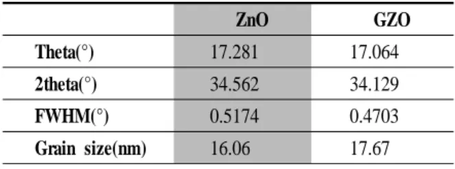
ZnO GZO
Theta(°) 17.281 17.064
2theta(°) 34.562 34.129
FWHM(°) 0.5174 0.4703
Grain size(nm) 16.06 17.67 Figure 1 shows the TEM images of ZnO and GZO
films deposited on a glass substrate. The thicknesses of the ZnO and GZO films were measured to be about 500 nm determined by TEM. The ZnO film has a less dense structure with pores between the grains as a result of the low atomic mobility, which is indicated by the arrows [7]. On the other hand, the GZO film showed a pore free film, as shown in Figure 1(b). The columnar structure of the GZO film was more stable than the ZnO film, resulting in the enhanced crystalline quality.
Figure 2. X-ray diffraction spectra of ZnO and GZO on glass substrates
Figure 2 shows the results of high-resolution X-ray diffraction measurements using a 2θ scan with Cu Kα1. The (002) peak position was observed at 2θ of
~ 34.30˚ for all samples. As shown in Fig. 2, the ZnO and GZO films prepared by rf magnetron sputtering are polycrystalline with a hexagonal structure and showing a preferred orientation perpendicular to the substrate surface. After Ga doping, the diffraction peak became more intense and the full width at half maximum (FWHM) of diffraction peaks was reduced, which indicate that the crystalline quality of GZO film was improved compared to that of ZnO film due to Ga doping. It was also found that the average grain size of GZO film was increased.
Table 1. FWHM and Grain size from XRD data.
Tabel 1 shows the FWHMs and average grain sizes for both ZnO and GZO films. The GZO film demonstrated the highest peak intensity. The grain size was estimated using the Scherrer’s equation and it was found that the grain size of ZnO and GZO was about 16.06 and 17.67 nm, respectively [8]. As the grain size increase, the optical conductivity is improved[9]. From figure 2, it is obvious that the (002) peak position for GZO film was shifted compared to that of ZnO film. We believe that it is attributed to the Ga doping. This indicates that the stress exists in the films along with the c-axis. If there exists the tensile stress in the film, the lattice spacing increase and the diffraction angle decreases.
On the other hand, If there exists the compressive stress in the film, the lattice spacing decreases and the diffraction angle increases. Ga-doping lead to tensile stress in ZnO films on glass. Due to the inner tensile stress, the crystal lattice mismatch between substrates and ZnO film decreases[10].
Figure 3. Optical transmission spectra of ZnO(○) and
GZO(△) films deposited on glass at room
temperature.
The transmittance spectra for both ZnO and GZO as a function of wavelength in the range 200-1400 nm is shown in figure 3. Optical transmittance of the GZO film was found to be increased by Ga-doping compared to that of ZnO film. In the GZO film, the average transmittance is over 80% in the visible region, which is about 10% higher than that of ZnO film. It was also observed that the optical absorption edge of GZO film became steeper than that of ZnO film. It demonstrates that the surface of GZO is smoother than that of ZnO[11]. Therefore, we believe that higher optical transmittance could be obtained by Ga doping, which is suitable for the application of GZO as a candidate for the transparent electrode.
Figure4. PL spectra of ZnO(▲) and GZO(○) films deposited on glass.
PL spectra obtained at room temperature are shown in Fig. 4. Those spectra display two emission lines.
The emission peak in the UV region around 380 nm (3.26 eV) is from the near band edge (NBE) due to exciton recombination. The other is the deep level (DL) emission in the green range (~2.3 eV) [12,13].
The DL emission, which has been the subject of many speculations, is mainly attributed by defects such as zinc or oxygen vacancies. As can be seen in Fig. 4, for ZnO film, the DL emission line is nearly as intense as the NBE line. The peak intensity ratio of
NBE over the DL for ZnO film was 1.27. On the other hand, the peak intensity ratio of the NBE over the DL for GZO film was increased to 2.6, indicating an improvement of the optical quality. Ga atom with a smaller ionic radius than Zn can easily reduce the number of Zn vacancies, leading to a decrease of the DL emission [14-17]. The full-width at half-maximum (FWHM) of NBE emission for GZO was about 241.8 meV, which was slightly narrower than that of ZnO film with 250.3 meV. Considering our samples grown on glass substrates at room temperature without post heat treatment, those samples show reasonable crystalline qualities compared to other reports [18, 19]. The resistivities of ZnO and GZO films were measured to be 1.61 and 1.27 Ω•cm, respectively, by using the Hall measurements. The free carrier concentrations of ZnO and GZO films were approximately 1018 and 1020 cm2/Vs, respectively.
Ⅳ. Conclusions
Polycrystalline ZnO and Ga-doped ZnO (GZO) films were deposited by radio frequency (rf) magnetron sputtering at room temperature. The XRD data confirmed the formation of highly oriented ZnO films in the direction of (002). According to the results of our experiments, the transmittance of the GZO film was enhanced by 10% from that of the ZnO film. From photoluminescence (PL) data, the ratio of intensity of near band edge (NBE) emission to deep level (DL) emission was as high as 2.65:1 and 1.27:1 in the GZO and ZnO films, respectively. We noted a decrease in the resistivity of GZO films, which occurred due to the activation of Ga dopants. And the carrier concentrations of ZnO and GZO film were approximately 1018 and 1020 ㎠/Vs, respectively.
These enhanced electrical and optical properties of
GZO thin films could be explained as that doped Ga
atoms were fully activated by translation from
interstitial to substitutional sites.
Acknowledgment
J. M thanks the Korea Science and Engineering Foundation (KOSEF) through the National Research Lab. Program funded by the Ministry of Science and Technology (No. R0A-2005-000-10011-0).
Reference
[1] K. Ellmer, J. Phys. D. Appl. Phys. 34, 3097 (2001).
[2] T. Minami, MRS Bull. 25, 38 (2000).
[3] H. J. Ko, Y. F. Chen, S. K. Hong, H. Wenisch and T. Yao, Appl. Phys. Lett. 77, 3761 (2000).
[4] R. G. Gordon, MRS Bull. 25, 52 (2000).
[5] J. H and. G. Gordon, J. Appl. Phys. 72 , 5381 (1992).
[6] H. L. Hartnagel, A. L. Dawar, A. K. Jain and C.
Jagadish, Semiconducting Transparent Thin Film (Institute of Physics Publ, Bristol, 1995).
[7] D. C. Kim, B. H. Kong and H. K Cho, phys. stat.
sol. (b) 244, 1512 (2007).
[8] H. P. Klug and L. Alexander, X-Ray Diffraction Procedures for Polycrystalline and Amorphous Materials (2nd ed.), (John Wiley and Sons, NewYork 1974).
[9] Q. P. wang, D. H Zhang and H. L Ma, Applied Surface Science 220, 12 (2003).
[10] K. SHIMAKAWA and T. ITOH, Jpn. J. Appl. Phys.
46, L577 (2007).
[11] X. Yu, J. Ma, F. Ji and Y. Qang, Thin Solid films 483 (2005)
[12] S. A. Studenikin, N. Golego and M. Cocivera, J .Appl. Phys. 84, 2287 (1998).
[13] X. H. Wang, D. X. Zhao, Y. C. Liu, J. Y. Zhang, Y. M. Lu and X. W. Fan, J. Cryst. Growth 263, 316 (2004).
[14] T. Minami, H. Sato, H. Nanto and S. Takata, Jpn.
J. Appl. Phys. 24, L781 (1985).
[15] O. F. Schirmer and D. Zwingel, Solid State Commun. 8, 1559 (1970).
[16] D. M. Bagnell, Y. F. Chen, M. Y. Shen, Z. Zhu, T. Goto and T. Yao, J. Cryst. Growth 184/185, 605 (1998).
[17] K. Vandheusen, W. L. Warren, C. H. Seager, D.
R. Tallant, J. A. Voigt and B. N. Gnage, J. Appl.
Phys. 79, 7983 (1996).
[18] Y. Ma, G. Du, J. Yin, T. Yang and Y. Zhang, Semicond. Sci. Technol. 20, 1198 (2005).
[19] J. CHO, J. NAH, M. S OH, J. H. SONG, K. H YOON, H. J. JUNG and W. K CHOI, Jpn. J. Appl.
Phys. 40, L1040 (2001).
RF 마그네트론 스퍼터링 방법으로 상온에서 유리기판 위에 성장시킨 ZnO의 성질에 미치는 Ga 도핑 효과
김금채1ㆍ이지수1ㆍ이수경1ㆍ김도현1ㆍ이성희2ㆍ문주호2ㆍ전민현1ϯ
1ϯ
인제대학교 나노시스템공학과 나노매뉴팩쳐링연구소, 김해 621-749
2
연세대학교 재료공학과, 서울 120-749
(2008년 1월 10일 받음)
유리기판 위에 약 500 nm 의 두께로 성장된 ZnO층의 구조적, 광학적, 전기적 성질에 미치는 갈륨도핑의 영향에 대하여 연구 하였다. 다결정 ZnO 와 GZO 층은 상온에서 radio frequency magnetron sputtering 법을 사용하여 성장되었다. 투과전자 현미경 (TEM)과 x-ray 회절분석 (XRD)에 의하면, 갈륨이 도핑된 ZnO 박막의 결정성은 ZnO에 비하여 향상되었고 (002)방 향을 따라 우선성장 되었음이 발견되었다. GZO 박막의 투과도는 가시광 영역에서 ZnO 박막에 비해 약 10% 정도 향상된 것 으로 나타났다. PL 분석에 따르면, NBE emission 세기와 DL emission 세기의 비는 GZO 와 ZnO의 경우 각각 2.65:1 과 1.27:1로 나타났다. GZO와 ZnO의 비저항은 각각 1.27과 1.61 Ω· cm 로서 GZO의 전기전도도가 높았다. GZO 와 ZnO의 캐 리어농도는 각각 1018 and 1020 ㎠/Vs으로 측정되었다. 본 실험결과 따르면, Ga 도핑으로 인해 ZnO 박막의 전기적, 광학적, 구조적 특성이 향상되었음을 알 수 있었다.
주제어 : zinc oxide (ZnO), 갈륨(Ga)이 도핑된 zinc oxide (GZO), 유리(Glass) 기판, 상온 성장, rf 마그네트론 스퍼터링