Regular Paper
587
J. KIEEMEVol. 26, No. 8, pp. 587-590, August 2013
DOI: http://dx.doi.org/10.4313/JKEM.2013.26.8.587
전기자동차 배터리 충전을 위한 DC - DC컨버터용 Super Junction MOSFET 설계에 관한 연구
김범준1, 홍영성1, 심관필2, 강이구3,a
1 극동대학교 정보통신학과
2 극동대학교 에너지반도체학과
3 극동대학교 태양광공학과
Study on the Design of DC-DC Converter for Super Junction MOSFET Battery Charger of Electric Vehicles
Bum June Kim
1, Young Sung Hong
1, Gwan Pil Sim
2, and Ey Goo Kang
3,a1 Department of Information & Telecommunication, Far East University, Eumseong 369-700, Korea
2 Department of Energy Semiconductor Engineering, Far East University, Eumseong 369-700, Korea
3 Department of Photovoltaic Engineering, Far East University, Eumseong 369-700, Korea
(Received July 17, 2013; Accepted July 22, 2013)
Abstract: Release competition and development of eco-friendly vehicles have been conducted violently also automaker, it will be a high growth industry of the charger and battery, which is the driving source of the motor of an electric vehicle. Reduces the on-resistance power elements DC - DC converter for battery charger for electric vehicles, must minimize switching losses. Should have a low on-resistance power than existing products. Compare the Super Junction MOSFET and Planar MOSFET, As a result, super junction MOSFET improve on about 87.4% on-state voltage drop performance than planar MOSFET.
Keywords: Planar, MOSFET, Charge balance, Pillar, Deep trench
1. 서 론1)
전 세계적으로 친환경 기술이 화두가 되고 있으며, 향후의 미래 산업을 이끌어갈 동력으로 여겨지고 있는 추세이다. “그린”이라는 용어는 지구 온난화를 방지하 기 위해 탄소배출량을 줄이자는 것으로부터 시작되었으 며 대부분의 업계에서 이를 위한 기술 개발을 추진 중
a. Corresponding author; [email protected]
Copyright ©2013 KIEEME. All rights reserved.This is an Open-Access article distributed under the terms of the Creative Commons Attribution Non-Commercial License (http://creativecommons.org/licenses/by-nc/3.0) which permits unrestricted non-commercial use, distribution, and reproduction in any medium, provided the original work is properly cited.
에 있다. 이에 따라 자동차 제조업체도 친환경 자동차 개발 및 출시 경쟁이 치열하게 벌어지고 있으며, 전기 자동차 모터의 구동원인 배터리 및 충전기 산업의 고성 장을 이룰 것이다. 전기자동차 배터리 충전기의 DC - DC 컨버터용 파워 소자로는 600 V/20 A급의 power MOSFET가 사용되어야 하지만, 기존의 power MOSFET 는 높은 온 저항으로 인해 구동 손실이 높아 사용에 어려 움이 있다. 이를 위하여 기존의 power MOSFET 대비 온 저항이 크게 낮아지는 super junction 구조를 통하여 기존 planar MOSFET과 비교하여 항복전압의 변화 없이 온 저항을 감소시켜 구동 손실 감소를 구현하고자 하 였다.
588 J. KIEEME, Vol. 26, No. 8, pp. 587-590, August 2013: B. J. Kim et al.
2. 실험 방법
2.1 Super junction MOSFET 이론적 고찰
Fig. 1. Planar and super junction power MOSFET electric field.
Super junction MOSFET의 경우 오프 상태에서 수 직 방향으로만 공핍층이 형성되는 planar MOSFET와 는 달리 수직 방향과 수평 방향으로 모두 공핍층을 형 성한다. 이것은 그림 1과 같이 P-필라 영역의 존재로 인하여 역방향 전압이 기존의 P-베이스와 N-드리프트 영역의 접합뿐만 아니라 P-필라와 N-드리프트 영역의 접합으로 확장되어 넓은 접합 면적에 인가되기 때문이 다. 항복전압 최적화를 위해서는 P-필라와 N-필라 영 역이 동시에 완전한 공핍화가 이루어져야 하고, 이를 위해서 P-필라와 N-드리프트 영역의 전하량이 식 (1) 을 만족하여 균형을 이루도록 설계되어야 한다 [1].
N
a, p i l l a rW
P= Nd, d r i f tW
N (1)식 1의 조건을 만족하는 super junction MOSFET 은 두 영역 간의 전하량이 동일하므로 P-필라와 N- 드리프트 영역 모두 완전 공핍화되어 그림 1과 같이 수평 방향으로 전계가 일정하게 발생한다.
2.2 Planar MOSFET 기본구조 설계
본 논문의 super junction MOSFET과 비교하기 위 한 planar MOSFET를 설계하여 표 1에 정리하였다.
Table 1. 600 V planar MOSFET optimization parameter.
Parameter Unit Condition
N-drift (Resistivity) Ω㎤ 18
JFET (Dose) ㎤ 1E12
P-Base (Dose) ㎤ 6.5E13
N+ Substrate
(Resistivity) Ω㎤ 0.018
P+ (Dose) ㎤ 3E15
N+ (Dose) ㎤ 5E15
Gate (Length) μm 4
Table 2. 600 V planar MOSFET optimization result.
Vth BV Rds(on)@(100 A/cm
2)
3.7 V 722 V 0.15 Ω cm
2Fig. 2. 600 V planar MOSFET optimization design.
N-드리프트 길이를 super junction MOSFET 구조 와 같이 설계하여 항복전압에 따른 온 저항의 차이를 비교할 수 있도록 60 μm로 설정하고 N-드리프트 비 저항, P-베이스 농도 변화를 통해 600 V에 최적화된 값을 도출해 내었다.
2.3 Super junction MOSFET 기본구조 설계
앞서 설계한 600 V planar MOSFET 구조에 super junction MOSFET 구조를 형성하여 N-필라 (N-드 리프트) P-필라의 영역을 구분하고 전하 균형을 맞추 어 최적화 설계를 진행하였다. 설계한 결과는 다음 표 3 및 그림 3과 같다.
기본적인 super junction MOSFET 공정 조건 중 P-필라와 N-드리프트 농도의 변화로 항복전압과 전 하 균형에 어떠한 영향을 나타내는지 알아보기 위하 여 시뮬레이션을 진행한 결과를 표 4와 그림 4에 도 시하였다.
전기전자재료학회논문지, 제26권 제8호 pp. 587-590, 2013년 8월: 김범준 등 589
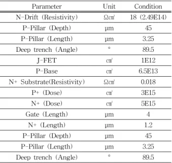
Parameter Unit Condition
N-Drift (Resistivity) Ω㎤ 18 (2.49E14)
P-Pillar (Depth) μm 45
P-Pillar (Length) μm 3.25
Deep trench (Angle) ° 89.5
J-FET ㎤ 1E12
P-Base ㎤ 6.5E13
N+ Substrate(Resistivity) Ω㎤ 0.018
P+ (Dose) ㎤ 3E15
N+ (Dose) ㎤ 5E15
Gate (Length) μm 4
N+ (Length) μm 1.2
P-Pillar (Depth) μm 45
P-Pillar (Length) μm 3.25
Deep trench (Angle) ° 89.5
Table 3. Super junction MOSFET parameter.
Fig. 3. Super junction MOSFET design.
Table 4. Breakdown voltage which forms the charge balance.
N-Drift (Resistivity)
N-Drift (Dose) P-Pillar (Dose) BV
0.1 Ω 8.09E16 2.19E15 37 V
~ ~ ~ ~
0.9 Ω 5.54E15 6.54E15 680 V
1.0 Ω 4.94E15
5.44E15 730 V
5.64E15 744 V
5.84E15 727 V
1.5 Ω 3.22E15 3.71E15 817 V
2.0 Ω 2.37E15 2.55E15 844 V
2.5 Ω 1.88E15 2.24E15 876 V
Fig. 4. P-pillar, N-drift resistivity graph.
Fig. 5. 600 V super junction MOSFET optimization design.
Table 5. 600 V super junction MOSFET optimization parameter.
Parameter Unit Condition
N-drift (Resistivity) Ω㎤ 1.0 (4.94E14)
P-Pillar (Dose) ㎤ 5.84E15
P-Pillar (Depth) μm 45
P-Pillar (Length) μm 3.25
Deep trench (Angle) ° 89.5
J-FET ㎤ 1E12
P-Base ㎤ 6.5E13
N+ Substrate (Resistivity) Ω㎤ 0.018
P+ (Dose) ㎤ 3E15
N+ (Dose) ㎤ 5E15
Gate (Length) μm 4
N+ (Length) μm 1.2
590 J. KIEEME, Vol. 26, No. 8, pp. 587-590, August 2013: B. J. Kim et al.
Table 6. 600 V super junction MOSFET optimization result.
Vth BV Rds(on)@(100 A/cm
2)
4.7 727 0.019 Ω cm
2N-드리프트 비저항을 0.1 Ω에서 2.5 Ω까지 단계 별로 변화시키며 시뮬레이션 한 결과, 그림 4에서 보듯이 비저항 이 높을수록 전하 균형을 이룰 때 항복전압도 비저항과 비 례하며 높아지는 경향성을 확인하였고, N-드리프트농도가 4.94E15, P-필라 농도가 5.84E15일 때 planar MOSFET와 같은 727 V의 항복전압을 가지는 것을 확인할 수 있었다.
3. 결과 및 고찰
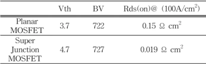
최적화된 planar MOSFET와 super junction MOSFET 의 특성 비교를 아래 그림 6과 표 7에 나타내었다.
(a)
(b)
(c)
Fig. 6. Threshold voltage, breakdown voltage, on resistance optimization in respect of planar, super junction (a) V
th, (b) BV, (c) R
on.Table 7. Threshold voltage, breakdown voltage, on resistance optimization in respect of planar, super junction.
Vth BV Rds(on)@ (100A/cm
2) Planar
MOSFET 3.7 722 0.15 Ω cm
2Super Junction MOSFET
4.7 727 0.019 Ω cm
2표에서 보다시피 같은 항복전압에서 super junction MOSFET이 온 저항이 큰 차이로 낮아짐을 볼 수 있었다.
4. 결 론
Super junction MOSFET 구조에서 최대 항복전압의 특성은 N-드리프트와 P-필라의 전하 균형을 통하여 이루 어지게 된다. Planar MOSFET에서 P-필라를 형성하여 전 하균형을 통해 항복전압이 향상되는 것을 확인하였으며 게이트 전압을 10 V로 설정하여 planar MOSFET와 super junction MOSFET 특성 비교를 그림 6에 나타내 었다. 그 결과 planar MOSFET과 동일한 항복전압을 유 지하면서 온 저항이 약 87.4% 향상된 0.019 Ω cm2이 나 타남을 알 수 있었으며 이로 인하여 온 저항 특성이 향 상되어 전력 소자의 손실 전력을 개선됨을 알 수 있었다.
감사의 글
본 논문은 산학협동재단의 학술연구비지원과제로 수행된 연구 결과입니다.
REFERENCES
[1] MOSFET Basics - Fairchild Semiconductor (2000).
[2] G. P. Sim, B. S. Ann, Y. H. Kang, Y. S. Hong, and E. G. Kang, J. KIEEME, 26, 190 (2013).
[3] H. S. Lee, E. G. Kang, A. Shin, H. H. Shin, and M.
Y. Sung, KIEE, 2006, (2006).
[4] Y. S. Hang, E. S. Jung, and E. Y. Kang, J.
KIEEME, 25, 276 (2012).