Sol ‐ gel growth and structural, electrical, and optical properties of vanadium ‐ based oxide thin films
Young Ran Park and Kwang Joo Kim
*Department of Physics, Konkuk University, Seoul 143‐701, Korea
(Received July 10, 2006)
Thin films of V2O3, VO2, and V2O5 were obtained from a single precursor solution through post‐annealing processes under different annealing conditions. As annealed in air, the deposited films became V2O5 with orthorhombic crystal structure, while they were V2O3 and VO2 with rhombohedral and monoclinic crystal structure as annealed in vacuums with base pressure of 1×10‐6 Torr and with 10 mTorr O2 pressure, respectively. Electrical and optical measurements indicated that the V2O5 and VO2
films are semiconducting, while the V2O3 films are metallic at room temperature.
Chromium doping in VO2 resulted in a decrease of the resistivity and changed the conduction type from n‐type to p‐type. 10% Cr‐doped VO2 films were found to have orthorhombic crystal structure, which is different from that of the undoped VO2. Spectral features in the optical absorption spectra of all the films were interpreted as the transitions involving O 2p and V 3d bands. The crystal‐field splittings between t2g
and eg states of the V 3d bands are estimated to be about 1.5 and 1.0 eV for V2O5 and VO2, respectively.
Keywords : Vanadium oxide, Sol‐gel, Structural properties, Optical properties
Ⅰ. Introduction
Recently, vanadium‐based oxides have been found to exhibit interesting physical and chemical properties applicable for sensors, catalysts, rechargeable batteries, and magneto‐
electronic devices etc. As the oxidation state of V ion increases from +3 to +5 in the compound VxOy, the electrical properties were found to vary from metallic to insulating at room temperature. V2O3 is known to undergo a Mott metal‐insulator (MI) transition along with a structural change from rhombohedral to monoclinic as the temperature decreases below 168 K [1]. For VO2 such MI transition occurs
near 341 K along with a tetragonal to monoclinic phase transformation [2,3]. V2O5
with the highest oxidation state of V ion is known to maintain structural stability with an orthorhombic structure. However, these oxides have not been well characterized in thin‐film form, despite the importance for device applications. Besides V2O3, VO2, and V2O5, there are many intermediate phases such as V3O5, V4O7, V5O9, V6O11, V7O13, V6O13, V4O9, and V3O7. Furthermore, the oxygen stoichiometry can be easily broken and the sample becomes either a form of VOx or a mixed phase.
In the present work, various vanadium oxide thin films have been prepared by a sol‐gel
method employing spin‐coating. Single‐phased V2O3, VO2, and V2O5 films could be obtained from a single precursor solution by varying post‐annealing condition on the spin‐coated film. A phase transformation was observed from monoclinic to orthorhombic structure by Cr doping on VO2. A decrease of the electrical resistivity as well as change of conduction type from n to p was also observed for the Cr‐
doped VO2 films. The optical constants of the vanadium‐oxide films were measured by spectroscopic ellipsometry (SE) in the visible‐
ultraviolet range and the observed absorption structures are interpreted in terms of transitions involving O 2p and V 3d states.
Ⅱ. Experimental
The precursor solution for V2O3, VO2, and V2O5 thin film fabrication by the present sol‐
gel method was prepared by dissolving (C5H8O2)2VO powder into a mixed solution of 2‐
methoxyethanol and monoethanolamine at 170
oC. For Cr or Fe doping Cr(NO3)3·9H2O or Fe(NO3)3·9H2O was dissolved together. The solution was spin‐coated on Al2O3(0001) substrate at 3000 rpm for 20 sec. Then the substrate was heated at 230 oC for 3 min after each deposition. This process was repeated for increasing the film thickness. The thickness of the present films was about 1 μm, estimated by scanning electron microscopy. The deposited films became V2O3, VO2, and V2O5 depending on the post‐annealing condition such as temperature and O2‐gas partial pressure.
The crystalline structure of the deposited films was investigated by X‐ray diffraction (XRD) measurements using Cu Kα radiation.
The transport properties of the films were investigated by Hall effect measurements, performed in the van der Pauw configuration under a magnetic field of 0.5 T. Optical
constants of the films were measured by SE at room temperature with a rotating‐analyzer ellipsometer in the visible‐ultraviolet range with the energy interval of 0.02 eV.
Ellipsometry measures the amplitude and the phase of the complex reflectance ratio ρ (= rp/rs) of the p (parallel) and s (perpendicular) field components of the light beam defined with respect to the plane of incidence of the sample. Then the dielectric function ε (= ε1 + i ε2) of the sample is obtained from the equation
2 2 2 1 2
sin sin tan ( ) 1
ε φ φ φ ρ
ρ
= + −
+ (1)
by assuming an optically flat boundary between the sample and the air. All the spectra were taken at an angle of incidence (φ) of 70o and a fixed polarizer angle of 45o from the plane of incidence.
Ⅲ. Results and discussion
When the as‐deposited precursor films were annealed in ambient air, V2O5 films with orthorhombic structure were produced in the 300 − 800 oC annealing temperature range as exhibited by the XRD spectra in Fig. 1. The spin‐coated precursor films showed amorphous phase with no observable XRD peak. The V2O5
films obtained at and above 500 oC are seen to be fairly oriented with the crystallographic c‐
axis of the orthorhombic structure perpen- dicular to the substrate surface and have lattice constants close to the bulk values. On the other hand, when the as‐deposited films were annealed in vacuum with the base pressure of 1×10‐6 Torr, V2O3 films with rhombohedral structure were produced as exhibited by the XRD spectra in Fig. 2. It is also seen that V2‐xFexO3 (x = 0.25) films
20 30 40 50 60 pure V2O5
(110) (101)
800oC
500oC 300oC
(001)
Intensity (arb. units)
2θ (deg.) 20 30 40 50 60 70
(300) (214) (116)
(024) (113) (006) (110) (104)
(012)
pure V2O3 Fe0.25V1.75O3
Intensity (arb. units)
2θ (deg.) 50 100 150 200 250 300
0 50 100 150 200 250 300 350
heating cooling
pure V2O3
σ (Ω-1 cm-1 )
Temperature (K) Fig. 1. XRD spectra of or-
thorhombic V2O5 films sol‐gel prepared and annealed in air at dif- ferent temperatures.
Fig. 2. XRD spectra of rhombohedral V2O3 and V2‐xFexO3 (x = 0.25) films.
Fig. 3. Temperature dependence of elec- trical conductivity of rhombohedral V2O3 film.
prepared under the same annealing condition maintain the rhombohedral structure with little change of lattice constants. Closeness of substituting Fe3+ ionic radius (0.785 Å) to that of V3+ (0.780 Å) is attributable to the result [4]. As shown in Fig. 3, the V2O3 film exhibits a MI transition near 190 K (marked by an arrow), a higher temperature than that reported for a bulk. It is attributable to finite grain size of the film. Also, a hysteresis behavior is observed between cooling and heating with conductivity of 160 (cooling) and 110 Ω-1
⋅
cm-1 (heating) at 150 K.In order to obtain VO2 films, O2 gas was supplied during the vacuum‐annealing process.
Due to the temperature‐sensitiveness of the crystal structure of VO2, the vacuum‐annealed films used to contain both monoclinic (semiconducting) and tetragonal (metallic) structures. Figure 4 exhibits the variation of the XRD spectrum of the VO2 films near 28o for different annealing condition. Pure monoclinic phase is obtained at particular O2‐ gas partial pressure (10 mTorr) and annealing temperature (650oC). Films with pure tetra- gonal phase were not obtained.
25 26 27 28 29 30
pure VO2
(d)
(c)
(b)
(a)
(011) (11-1)
(110)
Intensity (arb. units)
2θ (deg.)
Fig. 4. XRD spectra of VO2 films obtained by vac- uum annealing under different condition:
600 oC, 2 hr (a) 800 oC, 2 hr (b) 600 oC, 2 hr with O2 supply (10 mTorr) (c) 650 oC, 10 hr with O2 supply (10 mTorr) (d). The (011) and (11‐1) peaks are from monoclinic phase and the (110) peak is from tetragonal phase.
Hall measurements on the V2O5 and VO2
films at room temperature revealed that they have n‐type semiconducting properties with carrier concentration (resistivity) of about 9×1015 cm‐3 (3×10² Ωㆍcm) and 1×1016 cm‐3 (3×101 Ωㆍcm), respectively. The carrier mobility of the VO2 films is estimated to be around 20 cm2/Voltㆍsec, larger than that of
20 40 60 80
(400) (131) (331) (111)
(020) (200)
(202) (402) (022) (211) (102) (021) (210) (002) (200) (011)
V0.9Cr0.1O2
pure VO2 (b)
(a)
Intensity (arb. units)
2θ (deg.) 02.0 2.5 3.0 3.5 4.0 4.5 5.0 1
2 3 4 5 6 7 8
pure V2O5 ε1 ε2
ε 1 & ε 2
Photon Energy (eV) Fig. 5. Comparison of XRD spectra of
pure VO2 film with monoclinic structure (a) and V1‐xCrxO2 (x = 0.1) with orthorhombic structure (b).
Fig. 6. Real and imaginary part of the di- electric function of orthorhombic V2O5 film measured by SE.
the V2O5 films by a factor of 10. On the other hand, the V2O3 films exhibit semi‐metallic properties at room temperature with resistivity of about 3×10‐3 Ωㆍcm. When Cr was doped into VO2, a change in the electrical properties was observed. VO2 film samples doped by 2 at.% Cr showed p‐type character with enhanced (reduced) carrier concentration (resistivity) of 1×1020 cm‐3 (2 Ωㆍcm) compared to that of pure VO2. The V ion in VO2 has a nominal valence of +4. Thus, the exhibited p‐type conductivity of the VO2:Cr film indicates that the substituting Cr ions for the octahedral V sites have a valence of +3. Due to the structural instability of VO2 the crystal structure of the Cr‐doped films (V1‐xCrxO2) exhibits a phase transition to orthorhombic structure for x = 0.1 as shown in Fig. 5.
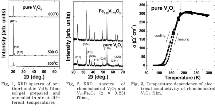
Figure 6 shows the real (ε1) and imaginary (ε
2) parts of the dielectric function of an orthorhombic V2O5 film (annealed at 500 oC) measured by SE. It is seen that the optical absorption starts at about 2.3 eV, considered to be the band‐gap energy of V2O5 [5]. The band‐gap absorption of V2O5 has been interpreted as due to the conduction‐band edge
originated from the empty V 3d state and the valence‐band edge consisting of O 2p states.
According to the result of a band‐structure calculation for orthorhombic V2O5, d bands are empty with the eg bands being located at higher energies than the t2g bands due to octahedral configuration of V ions. Also, a portion of them with t2g(dxy,dyz) character equivalent to one electron state is located at lower energies compared to the rest of the d bands by about 0.6 eV [6]. The observed band‐
gap absorption is interpreted as due to the transition from the valence‐band edge with O 2p character to such t2g(dxy,dyz) bands. Also, the exciton‐like absorption peak at about 3 eV is interpreted as due to the transition to the main high‐density d(t2g) band edge from the O 2p bands. The broad absorption structure at about 4.5 eV can be explained in terms of the transition to the d(eg) bands from the O 2p bands. From the present optical data the energy difference between the center of the eg
and the t2g bands, i.e., the crystal‐field (CF) splitting of the octahedral V5+ ion in orthor- hombic V2O5, is estimated to be about 1.5 eV.
Figure 7 exhibits the real and imaginary
1.5 2.0 2.5 3.0 3.5 4.0 4.5 5.0 0
1 2 3 4 5 6 7 8 9 10
pure VO2 ε1 ε2
ε 1 & ε 2
Photon Energy (eV)
1.5 2.0 2.5 3.0 3.5 4.0 4.5 5.0 1
2 3 4 5 6
pure V2O3 ε1 ε2
ε 1 & ε 2
Photon Energy (eV) Fig. 7. Real and imaginary part of the di-
electric function of monoclinic VO2 film measured by SE.
Fig. 9. Real and imaginary part of the di- electric function of rhombohedral V2O3 film measured by SE.
part of the dielectric function of a monoclinic VO2 film. In semiconducting VO2 optical absorption exists at low energies below 2 eV while no absorption exists for V2O5 in the same energy range. Also, strong absorption structures are observed at about 2 and 3 eV.
For VO2 a part of the d band is filled and a Mott‐Hubbard‐type band gap is expected to open up between the filled and the empty d(t2g) bands with a size of about 0.6 eV for the monoclinic structure [7]. Thus, VO2 is expected to exhibit finite optical absorption strength above 0.7 eV while V2O5 does not.
The 2‐ and 3‐eV absorption peaks are interpreted as due to the 2p → d(t2g) and 2p
→ d(eg), respectively. Thus, the energy difference between the center of the eg and t2g
bands, i.e., the CF splitting of the octahedral V4+ ion in monoclinic VO2, is estimated to be about 1.0 eV, being reduced compared to that of the orthorhombic V2O5. A simplified electronic band structure diagram for V2O5 and VO2 containing optical transitions and CF splittings is exhibited in Fig. 8.
Figure 9 exhibits the real and imaginary part of the dielectric function of a rhombo- hedral V2O3 film. The dielectric function of
V2O3 shows strong absorption structures at low energies, interpreted as due to its semi‐
metallic nature at room temperature. The smaller magnitude of the real part of the dielectric function of V2O3 than those of VO2
and V2O5 at low energies also reflects the metallic properties of V2O3 at room temperature.
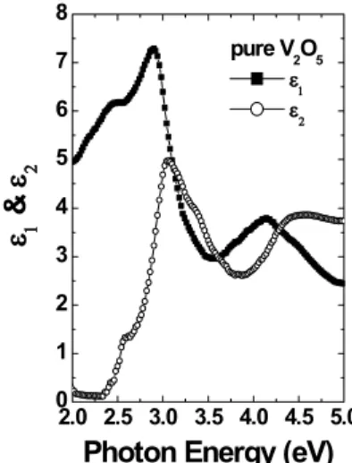
Fig. 8. Simplified electronic energy‐band structure diagram for V2O5 (a) and VO2 (b).
Ⅳ. Conclusion
Orthorhombic V2O5, monoclinic VO2, and rhombohedral V2O3 thin films have been prepared by sol‐gel method from single precursor solution. Annealing temperature and O2‐gas partial pressure during the post‐
annealing process were found to determine the crystal structure of the resultant films. The V2O5 and VO2 films exhibited n‐type semiconducting properties while the V2O3 films metallic properties investigated by Hall and SE measurements. Cr doping in VO2 resulted in a change of conductivity type from n to p as well as a phase transformation from monoclinic to orthorhombic structure. The dielectric functions of the V2O5 and VO2 films measured by SE revealed that the CF splitting between the eg and the t2g bands is about 1.5 and 1.0 eV, respectively.
Acknowledgment
This work was supported by the financial support of Konkuk University made in the program year of 2005.
References
[1] D. B. McWhan and J. P. Remeika, Phys.
Rev. B 2, 3734 (1970).
[2] F. J. Morin, Phys. Rev. Lett. 3, 34 (1959).
[3] H.‐T. Kim, B.‐G. Chae, D.‐H. Youn, S.‐L.
Maeng, G. Kim, K.‐Y. Kang, and Y.‐S.
Lim, New J. Phys. 6, 52 (2004).
[4] R. D. Shannon, Acta Crystallogr., Sect. A 32, 751 (1976).
[5] M. Losurdo, G. Bruno, D. Barreca, and E.
Tondello, Appl. Phys. Lett. 77, 1129 (2000).
[6] J. C. Parker, D. J. Lam, Y.‐N. Xu, and W.
Y. Ching, Phys. Rev. B 42, 5289 (1990).
[7] A. Bianconi, S. Stizza, and R. Bernardini, Phys. Rev. B 24, 4406 (1981).
바나듐 옥사이드 박막의 성장 및 그 구조적 , 전기적 , 광학적 특성
박영란ㆍ김광주*
건국대학교 물리학과, 서울시 광진구 화양동 1번지, 143-701 (2006년 7월 10일 받음)
V2O3, VO2, V2O5 박막들이 하나의 선구 용액으로부터 다양한 후열처리 조건을 통하여 제작될 수 있었다. 진공 중 후열처리 시 rhombohedral 구조의 V2O3 박막이 형성되어졌고, 공기 중 후열처리 시 orthorhombic 구조의 V2O5
박막을 얻을 수 있었다. Monoclinic 구조의 VO2 박막은 진공 후열처리 중 O2
가스를 공급함으로써 제작될 수 있었다. V2O3 박막이 상온에서 도체적 특성을 보이는 반면, V2O5, VO2 박막은 반도체적 성질을 지니고 있음을 전기적, 광학적 특성 조사를 통하여 알 수 있었다. 크롬(Cr)이 도핑됨에 따라 VO2
박막은 그 전기전도성이 n‐type에서 p‐type으로 변화하였고 비저항이 감소되는 결과를 나타내었다. 또한, 크롬 도핑된 VO2 박막은 orthorhombic 구조를 나타내었다. 이와 같은 바나듐 옥사이드 박막들에서 관측된 광학적 흡수 구조들은 O 2p 에서 V 3d 밴드로의 전이에 의한 것으로 해석되어진다. 바나듐 이온의 t2g 상태와 eg 상태 사이의 결정장 갈라짐(crystal‐field splitting)은 V2O5와 VO2에 대해서 각각 1.5 및 1.0 eV로 해석된다.
주제어 : 바나듐 옥사이드; 졸‐겔 방법; 구조적 특성; 광학적 특성
* [전자우편] [email protected]